Note: Descriptions are shown in the official language in which they were submitted.
1
ELECTROSURGICAL APPARATUS
FIELD OF THE INVENTION
The invention relates to electrosurgical apparatus in
which radiofrequency energy and microwave frequency energy are
used to treat biological tissue. In particular, the invention
relates to surgical apparatus capable of generating
radiofrequency (RF) energy for cutting tissue and microwave
frequency energy for haemostasis (i.e. sealing broken blood
vessels by promoting blood coagulation).
BACKGROUND OF THE INVENTION
Surgical resection is a means of removing sections of
organs from within the human or animal body. Such organs may
be highly vascular. When tissue is cut (divided or
transected) small blood vessels called arterioles are damaged
or ruptured. Initial bleeding is followed by a coagulation
cascade where the blood is turned into a clot in an attempt to
plug the bleeding point. During an operation, it is desirable
for a patient to lose as little blood as possible, so various
devices have been developed in an attempt to provide blood
free cutting. For endoscopic procedures, it is also
undesirable for a bleed to occur and not to be dealt with as
soon as quickly as possible, or in an expedient manner, since
the blood flow may obscure the operator's vision, which may
lead to the procedure needing to be terminated and another
method used instead, e.g. open surgery.
Instead of a sharp blade, it is known to use
radiofrequency (RF) energy to cut biological tissue. The
method of cutting using RF energy operates using the principle
that as an electric current passes through a tissue matrix
(aided by the ionic contents of the cells), the impedance to
the flow of electrons across the tissue generates heat. When a
CA 3060535 2019-10-29
2
pure sine wave is applied to the tissue matrix, enough heat is
generated within the cells to vaporise the water content of
the tissue. There is thus a huge rise in the internal
pressure of the cell, that cannot be controlled by the cell
membrane, resulting in the cell rupturing. When this occurs
over a wide area it can be seen that tissue has been
transected.
Whilst the above principle works elegantly in lean
tissue, it is less efficient in fatty tissue because there are
fewer ionic constituents to aid the passage of electrons.
This means that the energy required to vaporise the contents
of the cells is much greater, as the latent heat of
vaporisation of fat is much greater than that of water.
RF coagulation operates by applying a less efficient
waveform to the tissue, whereby instead of being vaporised,
the cell contents are heated to around 65 C. This dries out
the tissue by desiccation and also denatures the proteins in
the walls of vessels and the collagen that makes up the cell
wall. Denaturing the proteins acts as a stimulus to the
coagulation cascade, so clotting is enhanced. At the same
time the collagen in the wall is denatured and changes from a
rod like molecule to a coil, which causes the vessel to
contract and reduce in size, giving the clot an anchor point,
and a smaller area to plug.
However, RF coagulation is less efficient when fatty
tissue is present because the electrical effect is diminished.
It can thus be very difficult to seal fatty bleeders. Instead
of having clean white margins, the tissue has a blackened,
burned appearance.
In practice, a RF device may operate using a waveform
with a medium crest factor that is midway between a cutting
and coagulating output.
GB 2 486 343 discloses a control system for an
electrosurgical apparatus in which the energy delivery profile
of both RF energy and microwave energy delivered to a probe is
CA 3060535 2019-10-29
3
set based on sampled voltage and current information of RF
energy conveyed to the probe and sampled forward and reflected
power information for the microwave energy conveyed to and
from the probe.
Fig. 1 shows a schematic diagram of an electrosurgical
apparatus 400 as set out in GB 2 486 343. The apparatus
comprises a RF channel and a microwave channel. The RF
channel contains components for generating and controlling an
RF frequency electromagnetic signal at a power level suitable
for treating (e.g. cutting or desiccating) biological tissue.
The microwave channel contains components for generating and
controlling a microwave frequency electromagnetic signal at a
power level suitable for treating (e.g. coagulating or
ablating) biological tissue.
The microwave channel has a microwave frequency source
402 followed by a power splitter 424 (e.g. a 3 dB power
splitter), which divides the signal from the source 402 into
two branches. One branch from the power splitter 424 forms a
microwave channel, which has a power control module comprising
a variable attenuator 404 controlled by controller 406 via
control signal Vn and a signal modulator 408 controlled by
controller 406 via control signal VII, and an amplifier module
comprising drive amplifier 410 and power amplifier 412 for
generating forward microwave EM radiation for delivery from a
probe 420 at a power level suitable for treatment. After the
amplifier module, the microwave channel continues with a
microwave signal coupling module (which forms part of a
microwave signal detector) comprising a circulator 416
connected to deliver microwave EM energy from the source to
the probe along a path between its first and second ports, a
forward coupler 414 at the first port of the circulator 416,
and a reflected coupler 418 at the third port of the
circulator 416. After passing through the reflected coupler,
the microwave EM energy from the third port is absorbed in a
power dump load 422. The microwave signal coupling module
CA 3060535 2019-10-29
4
also includes a switch 415 operated by the controller 406 via
control signal V12 for connecting either the forward coupled
signal or the reflected coupled signal to a heterodyne
receiver for detection
The other branch from the power splitter 424 forms a
measurement channel. The measurement channel bypasses the
amplifying line-up on the microwave channel, and hence is
arranged to deliver a low power signal from the probe. In
this embodiment, a primary channel selection switch 426
controlled by the controller 406 via control signal Vfl is
operable to select a signal from either the microwave channel
or the measurement channel to deliver to the probe. A high
band pass filter 427 is connected between the primary channel
selection switch 426 and the probe 420 to protect the
microwave signal generator from low frequency RF signals.
The measurement channel includes components arranged to
detect the phase and magnitude of power reflected from the
probe, which may yield information about the material e.g.
biological tissue present at the distal end of the probe. The
measurement channel comprises a circulator 428 connected to
deliver microwave EM energy from the source 402 to the probe
along a path between its first and second ports. A reflected
signal returned from the probe is directed into the third port
of the circulator 428. The circulator 428 is used to provide
isolation between the forward signal and the reflected signal
to facilitate accurate measurement. However, as the
circulator does not provide complete isolation between its
first and third ports, i.e. some of the forward signal may
break through to the third port and interfere with the
reflected signal, a carrier cancellation circuit is used that
injects a portion of the forward signal (from forward coupler
430) back into the signal coming out of the third port (via
injection coupler 432). The carrier cancellation circuit
include a phase adjustor 434 to ensure that the injected
portion is 180 out of phase with any signal that breaks
CA 3060535 2019-10-29
5
through into the third port from the first port in order to
cancel it out. The carrier cancellation circuit also include
a signal attenuator 436 to ensure that the magnitude of the
injected portion is the same as any breakthrough signal.
To compensate for any drift in the forward signal, a
forward coupler 438 is provided on the measurement channel.
The coupled output of the forward coupler 438 and the
reflected signal from the third port of the circulator 428 are
connected to respective input terminal of a switch 440, which
is operated by the controller 406 via control signal V14 to
connect either the coupled forward signal or the reflected
signal to a heterodyne receiver for detection.
The output of the switch 440 (i.e. the output from the
measurement channel) and the output of the switch 415 (i.e.
the output from the microwave channel) are connect to a
respective input terminal of a secondary channel selection
switch 442, which is operable by the controller 406 via
control signal V15 in conjunction with the primary channel
selection switch to ensure that the output of the measurement
channel is connected to the heterodyne receiver when the
measurement channel is supplying energy to the probe and that
the output of the microwave channel is connected to the
heterodyne receiver when the microwave channel is supplying
energy to the probe.
The heterodyne receiver is used to extract the phase and
magnitude information from the signal output by the secondary
channel selection switch 442. A single heterodyne receiver is
shown in this system, but a double heterodyne receiver
(containing two local oscillators and mixers) to mix the
source frequency down twice before the signal enters the
controller may be used if necessary. The heterodyne receiver
comprises a local oscillator 444 and a mixer 448 for mixing
down the signal output by the secondary channel selection
switch 442. The frequency of the local oscillator signal is
selected so that the output from the mixer 448 is at an
CA 3060535 2019-10-29
6
intermediate frequency suitable to be received in the
controller 406. Band pass filters 446, 450 are provided to
protect the local oscillator 444 and the controller 406 from
the high frequency microwave signals.
The controller 406 receives the output of the heterodyne
receiver and determines (e.g. extracts) from it information
indicative of phase and magnitude of the forward and/or
reflected signals on the microwave or measurement channel.
This information can be used to control the delivery of high
power microwave EM radiation on the microwave channel or high
power RF EM radiation on the RF channel. A user may interact
with the controller 406 via a user interface 452, as discussed
above.
The RF channel shown in Fig. 1 comprises an RF frequency
source 454 connected to a gate driver 456 that is controlled
by the controller 406 via control signal V16. The gate driver
456 supplies an operation signal for an RF amplifier 458,
which is a half-bridge arrangement. The drain
voltage of the
half-bridge arrangement is controllable via a variable DC
supply 460. An output transformer 462 transfers the generated
RF signal on to a line for delivery to the probe 420. A low
pass, band pass, band stop or notch filter 464 is connected on
that line to protect the RF signal generator from high
frequency microwave signals.
A current transformer 466 is connected on the RF channel
to measure the current delivered to the tissue load. A
potential divider 468 (which may be tapped off the output
transformer) is used to measure the voltage. The output
signals from the potential divider 468 and current transformer
466 (i.e. voltage outputs indicative of voltage and current)
are connected directly to the controller 406 after
conditioning by respective buffer amplifiers 470, 472 and
voltage clamping Zener diodes 474, 476, 478, 480 (shown as
signals B and C in Fig. 1).
CA 3060535 2019-10-29
7
To derive phase information, the voltage and current
signals (B and C) are also connected to a phase comparator 482
(e.g. an EXOR gate) whose output voltage is integrated by RC
circuit 484 to produce a voltage output (shown as A in Fig. 1)
that is proportional to the phase difference between the
voltage and current waveforms. This voltage output (signal A)
is connected directly to the controller 406.
The microwave/measurement channel and RF channel are
connected to a signal combiner 114, which conveys both types
of signal separately or simultaneously along cable assembly
116 to the probe 420, from which it is delivered (e.g.
radiated) into the biological tissue of a patient.
SUMMARY OF THE INVENTION
The present invention provides an enhancement to the
electrosurgical apparatus disclosed GB 2 486 343. The
enhancement concerns the components used to isolate the probe
from the mains energy used to power the apparatus.
At its most general, the present invention proposes using
a waveguide isolator at the junction between the microwave
channel and signal combiner. The waveguide isolator may be
configured to perform three functions: (i) permit the passage
of very high microwave power (e.g. greater than 10 W); (ii)
block the passage of RF power; and (iii) provide a high
withstanding voltage (e.g. greater than 10 kV).
The invention may provide a capacitive structure at or
adjacent the waveguide that can reduce capacitive coupling
across the isolation barrier. The reduced capacitive coupling
may be provided by connecting the waveguide isolator (in
particular the outer conductor of the waveguide isolator) in
series with an additional capacitive component, such as a
coaxial isolator. To maintain the reduced capacitive coupling
during operation, the additional capacitive component may have
a high breakdown voltage, e.g. 500 V or more. Thus, the
CA 3060535 2019-10-29
8
waveguide isolator and additional capacitive component (e.g.
coaxial isolator) may act in combination as a low frequency
blocking filter to prevent RF EM radiation from the RF channel
from entering the microwave channel.
Alternatively, in a preferred embodiment the capacitive
structure may be an integral part of the DC isolation barrier
in the waveguide isolator itself. For example, reduced
capacitive coupling can be achieved by decreasing the
capacitance or increasing the capacitive reactance of the
isolating gap formed in the outer conductor of the waveguide
isolator, e.g. by increasing the thickness of insulating
material present in the gap. In this arrangement, the
waveguide isolator may include a choke to minimise leakage of
microwave power at the gap.
The advantage of using a waveguide isolator as described
above is that it both provides a high withstand voltage and
prevents unwanted capacitive coupling between the conductive
parts of the waveguide isolator. Without the reduced
capacitive coupling, there is a risk of a patient or user in
contact with the waveguide isolator forming part of a current
path resulting from the capacitive coupling, especially in the
outer conductor of the waveguide isolator. Such a risk may
affect the ability of the apparatus to meet the necessary
electrical safety standards for medical devices (e.g. as set
by International Electrotechnical Commission (IEC) standard
60601-2).
The invention effectively increases the capacitive
reactance of the isolation component and hence inhibits the
capacitive coupling.
According to the invention, there may be provided
electrosurgical apparatus for resection of biological tissue,
the apparatus comprising: a radiofrequency (RF) signal
generator for generating RF electromagnetic (EM) radiation
having a first frequency; a microwave signal generator for
generating microwave EM radiation having a second frequency
CA 3060535 2019-10-29
9
that is higher than the first frequency; a probe arranged to
deliver the RF EM radiation and the microwave EM radiation
separately or simultaneously from a distal end thereof; and a
feed structure for conveying the RF EM radiation and the
microwave EM radiation to the probe, the feed structure
comprising an RF channel for connecting the probe to the RF
signal generator, and a microwave channel for connecting the
probe to the microwave signal generator, wherein the RF
channel and microwave channel comprise physically separate
signal pathways from the RF signal generator and microwave
signal generator respectively, wherein the feed structure
includes a combining circuit having a first input connected to
the separate signal pathway on the RF channel, a second input
connected to the separate signal pathway on the microwave
channel, and an output connected to a common signal pathway
for conveying the RF EM radiation and the microwave EM
radiation separately or simultaneously along a single channel
to the probe, and wherein the microwave channel includes a
waveguide isolator connected to isolate the separate signal
pathway on the microwave channel from the RF EM radiation.
The waveguide isolator may comprise a conductive input
section, a conductive output section which mates with the
input section to define a waveguide cavity within a volume
enclosed by the input and output sections, and a DC isolation
barrier arranged between the input and output sections. The
waveguide cavity may be cylindrical. The output on the common
signal pathway may include a signal conductor and a ground
conductor, and the feed structure may include a capacitive
structure between the ground conductor of the output on the
common signal pathway and the conductive input section of the
waveguide isolator, the capacitive structure being arranged to
inhibit coupling of the RF EM energy and leakage of the
microwave EM energy.
As mentioned above, in a preferred embodiment the
capacitive structure may be provided by the DC isolation
CA 3060535 2019-10-29
10
barrier and a microwave choke formed on the input section of
the waveguide isolator. Where the inner and outer sections of
the waveguide isolator define a cylindrical body, the
microwave choke may comprise an annular channel extending
axially from the distal end of the inner section of the
waveguide isolator. The channel may be filled with air or
another suitable dielectric. The axial length of the choke
may be a quarter wavelength of the microwave EM energy (or an
odd multiple thereof) in the material (e.g. air) and
geometrical structure of the channel.
The DC isolation barrier itself may include a rigid
insulating spacer element mounted between the inner and outer
sections of the waveguide isolator. The spacer element may be
formed from an insulating plastic, such as Delrini0. In the
waveguide is cylindrical, the spacer element may comprise an
annular sleeve mounted over the distal end of one of the input
or output sections of the waveguide isolator. The outer
surface of the sleeve may be flush with the outer surface of
the input and output sections.
The axial length of the overlap between the sleeve and
the inner and/or outer sections is preferably an odd number of
quarter wavelengths (usually one quarter wavelength) at the
microwave frequency in the material of the sleeve and the
structure containing it. The thickness of the insulating
layer (radial thickness when it is an insulating sleeve) may
be selected to be either as thin as possible to minimise
microwave leakage or as thick as necessary to reduce the
capacitance to a level that provides the required isolation at
the frequency of the RF EM energy. These two requirements are
in conflict and it may be that they cannot both be met. In
practice, the sleeve may thus comprise either (i) a thin
insulating layer, which meets the microwave leakage
requirement but requires an additional capacitive break in
series with the outer conductor in order to reduce the
capacitance (e.g. the coaxial isolator discussed below), or
CA 3060535 2019-10-29
11
(ii) a thick insulating layer, which meets the RF REM energy
isolation requirement, but requires an additional microwave
component to achieve the required low microwave leakage (e.g.
the microwave choke discussed above).
The DC isolation barrier may includes additional
components. For example, the DC isolation barrier may include
an insulating film mounted on a portion of the inner surface
of the input section at the junction with the rigid insulating
spacer element. The insulating film may extend away from the
rigid insulating spacer element by a predetermined distance,
e.g. to increase the surface breakdown voltage.
The waveguide isolator allows the combining circuit to
float electrically, which increases safety. The capacitive
structure acts to increase the capacitive reactance of the
combining circuit to reduce the risk of an RF signal escaping
down the microwave channel via a capacitive coupling through
the waveguide isolator.
In another embodiment, the capacitive structure may
comprise an additional capacitance connected in series with
the waveguide isolator. The additional capacitance may be a
coaxial isolator. The additional capacitance may need to have
a high breakdown voltage to cope with the peak voltages seen
within the system. The breakdown voltage of the additional
capacitance may be 1 kV or more, preferably 2 kV or more.
Using the adapted waveguide isolator mentioned above or
the series-connected waveguide isolator and coaxial isolator
as a high pass filter may overcome three disadvantages of
using a single high frequency capacitor to provide the
necessary isolation. Firstly, it is desirable for the entire
combining circuit to be floating, i.e. without a direct path
to ground or the mains power. Thus, both the signal and
ground planes from the microwave channel need to enter the
combining circuit capacitively. The waveguide isolator can
provide this property. Secondly, it is desirable to prevent
the RF signal from leaking out to the patient or user through
CA 3060535 2019-10-29
12
capacitive coupling across the waveguide isolator. The
adapted DC Isolation barrier described above or the coaxial
isolator can provide the necessary capacitance to increase the
capacitive reactance of the junction and hence inhibit the
capacitive coupling at the first frequency. A coaxial
isolator is preferred to a normal capacitor because the RF
signal may be supplied as high voltage pulses (e.g. of 5 kV or
higher), which is higher than the typical voltage breakdown of
a normal capacitor. Thirdly, the insertion loss of the series
arrangement is much lower than for a normal capacitor at the
preferred microwave frequencies disclosed herein (e.g. 5.8 GHz
or higher), which can help to prevent the circuit resonating a
certain frequencies.
The invention may be combined with any or all of the
components (either individually or in any combination)
described above with reference to the electrosurgical
apparatus 400 as set out in GB 2 486 343. For example, the RF
channel and microwave channel may include any or all of the
components of the RF channel and microwave channel
respectively described above.
The separate signal pathway on the RF channel may be
isolated from the microwave EM radiation. The RF channel may
therefore include an isolator, e.g. a low pass, band pass,
band stop or notch filter, connected between the separate
signal pathway on the RF channel and the combining circuit.
The low pass, band pass, band stop or notch filter may be
integrated with the combining circuit. For example, in one
embodiment, the combining circuit may comprise a T-shaped open
microstrip bi-direction diplexer circuit having a low pass,
band pass, band stop or notch filter integrally formed
therewith to prevent microwave EM radiation from leaking out
of the first input. The band stop filter may comprise a
plurality of stubs (e.g. two, three or four stubs) formed on
the microstrip line between the first input and T-junction of
the diplexer circuit.
CA 3060535 2019-10-29
13
However, in a preferred embodiment the combining circuit
is integrated with the waveguide isolator. The separate
signal pathway on the RF channel may terminate at an RF
connector which is connected into the waveguide isolator,
whereby the RF signal is directly conveyed to an output port
of the waveguide isolator. The common signal pathway may thus
extend away from the output port of the waveguide isolator.
Thus, the output connected to common signal pathway may
include an output probe mounted on the output section of the
waveguide isolator, the output probe having a coupling
conductor extending into the waveguide isolator to couple the
microwave EM energy therefrom. The first input may include an
RF connector mounted on the waveguide isolator, the RF
connector having a signal conductor that extends into the
waveguide cavity to electrically contact the coupling
conductor of the output probe. The signal conductor may be an
insulated conductive wire or rod. The signal conductor may
contact the coupling conductor at a predetermined distance
from its tip. The distance may be adjustable, e.g. by
changing the position of the RF connected with respect to the
waveguide isolator. Preferably the position of the signal
conductor is aligned close to an equipotential of the
microwave EM energy within the microwave isolator, so the
presence of the RF connector does not affect the behaviour of
the microwave EM energy.
Integrating the combining circuit with the adapted
waveguide isolator provides a single component which provides
the necessary generator-to-patient isolation whilst avoiding
unwanted RF coupling and microwave leakage. In addition this
single component obviates the need for a separate multi-stub
(low pass) rejection filter on the RF channel. Moreover, the
integrated nature of the component means that the insertion
loss of the device is much lower (there is no microstrip
board, fewer interconnections, fewer microwave routing cables,
no co-axial isolator). The integrated waveguide isolator is
CA 3060535 2019-10-29
14
also physically smaller and easier to manufacture than the
multi-component solution.
The apparatus may include a controller operable to select
an energy delivery profile for the RF EM radiation and the
microwave EM radiation. Herein, energy delivery profile may
mean the shape of the waveform in terms of voltage/current and
time for the RF energy and power level and time for the
microwave energy. Control of the energy delivery profile can
permit a range of therapeutic applications to be realised.
The apparatus may include an RF signal detector for
sampling current and voltage on the RF channel and generating
therefrom a RF detection signal indicative of the phase
difference between the current and voltage. The controller
may be in communication with the RF signal detector to receive
the RF detection signal and select the energy delivery profile
for the RF EM radiation based on the RF detection signal.
Similarly, the apparatus may include a microwave signal
detector for sampling forward and reflected power on the
microwave channel and generating therefrom a microwave
detection signal indicative of the magnitude and/or phase of
microwave power delivered by the probe. The controller may be
in communication with the microwave signal detector to receive
the microwave detection signal and select the energy delivery
profile for the microwave EM radiation based on the microwave
detection signal.
Thus, the system may be configured to provide secure
control over the output of the electrosurgical apparatus. For
example, the apparatus may enable selection of an energy
delivery profile for tissue cutting which may comprise
delivering continuous wave (CW) RF EM energy with a 400 V peak
amplitude at a power level of 30 W. The controller may be
adjustable (e.g. manually adjustable) to vary the peak
amplitude and power level. Because the RF and microwave EM
radiation are monitored, the energy delivered to the tissue
can be determined with accuracy. In another example, the
CA 3060535 2019-10-29
15
apparatus may enable selection of an energy delivery profile
for coagulation may comprise delivering continuous wave (CW)
microwave EM energy at a power level of 25 W. Again, the
controller may be adjustable (e.g. manually adjustable) to
vary the power level.
More generally, to achieve tissue cutting in a dry
environment, it may be necessary to deliver a 500 kHz
continuous wave sinusoidal waveform with a peak voltage of
amplitude 400 V and a power setting of 40 W, whereas to
achieve tissue cutting in a wet environment, it may be
necessary to deliver one or more bursts of 500 kHz energy with
a peak voltage of 4000 V with a peak power of 200 W and a duty
cycle of 10%, which may be set up in the form whereby the ON
time is 10 ms and the OFF time is 90 ms. This kind of pulsed
energy delivery profile may ensure that the energy is passed
to the tissue rather than causing undesirable heating of the
surrounding fluid. For efficient tissue coagulation in dry
tissue, CW microwave power may be delivered into tissue at an
RMS power level of 30 W. For coagulation in a wet
environment, the microwave power may be pulsed, e.g. having a
peak power of 100 W with a 30% duty cycle.
Other waveforms that produce desirable therapeutic tissue
affects may include a combination of RF and microwave energy
delivered in CW and pulsed formats similar to those described
above. The RF and microwave energy may be delivered
simultaneously where the microwave energy modulates the RF
energy. For example, a 400 V peak 500 kHz CW RF profile may
be modulated with a 10 W CW 5.8 GHz microwave signal to
produce a degree of tissue coagulation during the resection
process to reduce bleeding when an organ or a section of an
organ is being removed.
All waveform parameters may be adjustable by the
controller, e.g. via a user interface.
The control system may comprise a dedicated measurement
channel, for delivering energy (preferably microwave energy)
CA 3060535 2019-10-29
16
at a low power level (e.g. 10 mW or less). The system may
thus make available measurement signals from a channel that is
not delivering therapeutic effects, i.e. the waveform or
energy delivery into tissue may be controlled based on low
power measurements made using a channel that is not involved
in delivering therapeutic tissue effects. The measurement
channel may be use the same source as the microwave channel.
The system may be switchable so that microwave energy is
delivered either through the measurement channel (in a
"measurement mode") or through the microwave channel (in a
"treatment mode"). Alternatively, the microwave channel may
be switchable between a low power mode (for measurement) and a
high power mode (for treatment). In this arrangement a
separate measurement channel is not needed.
The system may be configured to supply energy for cutting
and coagulating tissue simultaneously (e.g. a mixed or blend
mode) or may be operated independently, whereby the RF and
microwave energy is delivered to the probe under manual user
control (e.g. based on the operation of a footswitch pedal) or
automatically based on measured phase and/or magnitude
information from the RF and/or microwave channel. The system
may be used to perform tissue ablation and cutting. In the
instance where microwave and RF energy are delivered
simultaneously, either or both RF and microwave energy
returned to the respective generators may be used at high
power or low power to control the energy delivery profile. In
this instance, it may be desirable to take measurements during
the OFF time when the energy delivery format is pulsed.
The distal end of the probe may comprise a bipolar
emitting structure comprising a first conductor spatially
separated from a second conductor, the first and second
conductors being arranged to act: as active and return
electrodes respectively to convey the RF EM radiation by
conduction, and as an antenna or transformer to facilitate
radiation of the microwave EM energy. Thus, the system may be
CA 3060535 2019-10-29
17
arranged to provide a local return path for RF energy. For
example, the RF energy may pass by conduction through the
tissue separating the conductors, or a plasma may be generated
in the vicinity of the conductors to provide the local return
path. RF tissue cutting may be produced by a fixed dielectric
material separating the first and second conductors, where the
thickness of the dielectric material is small, i.e. less than
1 mm and the dielectric constant high, i.e. greater than that
of air.
The invention may be particularly suitable in
gastrointestinal (GI) procedures, e.g. to remove polyps on the
bowel, i.e. for endoscopic sub-mucosal resection. The
invention may also lend itself to precision endoscopic
procedures, i.e. precision endoscopic resection, and may be
used in ear, nose and throat procedures and liver resection.
The first frequency may be a stable fixed frequency in
the range 10 kHz to 300 MHz and the second frequency may be a
stable fixed frequency in the range 300 MHz to 100 GHz. The
first frequency should be high enough to prevent the energy
from causing nerve stimulation and low enough to prevent the
energy from causing tissue blanching or unnecessary thermal
margin or damage to the tissue structure. Preferred spot
frequencies for the first frequency include any one or more
of: 100 kHz, 250 kHz, 500 kHz, 1 MHz, 5 MHz. Preferred spot
frequencies for the second frequency include 915 MHz, 2.45
GHz, 5.8 GHz, 14.5 GHz, 24 GHz. Preferably the second
frequency is at least an order of magnitude (i.e. at least 10
times) higher than the first frequency.
In another aspect, the invention may be expressed as an
isolating circuit for electrosurgical apparatus for resection
of biological tissue, the isolating circuit comprising: a
combining circuit having a first input connectable to receive
radiofrequency (RF) electromagnetic (EM) radiation having a
first frequency from an RF channel, a second input connectable
to receive microwave EM radiation having a second frequency
CA 3060535 2019-10-29
18
that is higher than the first frequency from a microwave
channel, and an output in communication with the first and
second inputs for conveying the RE EM radiation and the
microwave EM radiation to a common signal pathway, and a
waveguide isolator connected to isolate the microwave channel
from the RF EM radiation, wherein the waveguide isolator
comprises a conductive input section, a conductive output
section which mates with the input section to define a
waveguide cavity within a volume enclosed by the input and
output sections, and a DC isolation barrier arranged between
the input and output sections, wherein the output from the
combining circuit includes a signal conductor and a ground
conductor, and wherein the isolating circuit comprises a
capacitive structure between the ground conductor of the
output from the combining circuit and the conductive input
section of the waveguide isolator, the capacitive structure
being arranged to inhibit coupling of the RE EM energy and
leakage of the microwave EM energy. Features of the combining
circuit, waveguide isolator and capacitive structure described
above may also be applicable to this aspect of the invention.
BRIEF DESCRIPTION OF THE DRAWINGS
Examples of the present invention are discussed in detail
below with reference to the accompanying drawings, in which:
Fig. 1 is an overall schematic system diagram of
electrosurgical apparatus in which the present invention may
be used, and is discussed above;
Fig. 2 is a schematic diagram of an isolating circuit in
an electrosurgical apparatus that is an embodiment of the
invention;
Fig. 3 is a schematic diagram of an isolating circuit
having only a waveguide isolator, for comparison with the
present invention;
CA 3060535 2019-10-29
19
Fig. 4 is a schematic diagram of an isolating circuit
according to the present invention, for comparison with Fig.
3;
Fig. 5 is a cross-sectional side view of a waveguide
isolator suitable for use in the invention;
Fig. 6 is an end view of the waveguide isolator shown in
Fig. 5;
Fig. 7 is a cross-sectional side view of a coaxial
isolator suitable for use in the invention;
Fig. 8 is a cross-sectional side view of the components
in the coaxial isolator shown in Fig. 7;
Fig. 9 is a schematic diagram of an isolating circuit in
an electrosurgical apparatus that is another embodiment of the
invention;
Fig. 10 is a cross-sectional side view of an adapted
waveguide isolator used in the isolating circuit of Fig. 9.
DETAILED DESCRIPTION; FURTHER OPTIONS AND PREFERENCES
Fig. 2 is a schematic diagram of an isolating circuit 200
for an electrosurgical apparatus that is an embodiment of the
invention. The isolating circuit 200 forms part of a feed
structure for conveying RF EM radiation from an RF signal
generator 218 and microwave radiation from a microwave signal
generator 220 to a probe. In this embodiment, the probe (not
shown) is connectable to an output port 228 provided in a
housing 226. The feed structure comprises an RF channel
having a RF signal pathway 212, 214 for conveying the RF EM
radiation and a microwave channel having a microwave signal
pathway 210 for conveying the microwave EM radiation. The
signal pathways for the RF EM radiation and microwave
radiation are physically separate from each other. The RF
signal generator is connected to the RF signal pathway 212,
214 via a voltage transformer 216. The secondary coil of the
transformer 216 (i.e. on the probe side of the arrangement) is
CA 3060535 2019-10-29
20
floating, so there is not direct current path between the
patient and the RF signal generator 218. This means that both
the signal conductor 212 and ground conductor 214 of the RF
signal pathway 212, 214 are floating.
A combining circuit 206 has a first input 203 for
connecting to the RF signal pathway 212, 214, and a second
input 205 for connecting to the microwave signal pathway 210.
The combining circuit 206 joins the pathways to an output 207,
which is connected to a common signal pathway 208. The common
signal pathway 208, which may include a flexible cable (e.g.
coaxial cable of the like) conveys the RF EM radiation and
microwave EM radiation to the probe. In this embodiment the
combining circuit 206 comprises a T-shaped microstrip junction
formed on a low loss microwave dielectric substrate (e.g. a
suitable type of RT/duroid substrate manufactured by Rogers
Corporation). The ground plane of the microstrip junction,
which is formed on the opposite side of the substrate from the
T-shaped microstrip junction, is connected to the ground
conductor 214 of the RF signal pathway 212, 214. It is
therefore floating. The T-shaped microstrip junction provides
the first input 203, which is connected to the signal
conductor 212 of the RF signal pathway.
A band stop filter 222 is provided on the T-shaped
microstrip junction in the form of three stubs 224 in shunt on
the microstrip line between the first input 203 and junction
223 with the microwave microstrip line. The stub nearest the
junction is spaced from it by an odd multiple of a quarter
wavelength of the microwave EM radiation transmitted by the
microstrip. The subsequent stubs are separated from one
another by half the wavelength. Using more than one stub
increase the effectiveness of the filter in preventing
microwave EM radiation from escaping into the RF pathway 212,
214.
The isolating circuit 200 comprises a waveguide isolator
202 and a coaxial isolator 204 connected in series on the
CA 3060535 2019-10-29
21
microwave signal pathway 210 between the microwave signal
generator 220 and second input 205. The waveguide isolator
202 and coaxial isolator 204 are effectively capacitors acting
as high pass filters. They permit microwave EM radiation from
the microwave signal generator 220 to pass to the combining
circuit 206, but prevent RF EM radiation from escaping back
out of the second input 205 of the combining circuit 206 into
the microwave signal generator 220.
In this embodiment, the microwave channel also include a
grounded stub 221 having a length equal to an odd multiple of
a quarter wavelength of the microwave EM radiation transmitted
by the microstrip to short out any residual RF EM radiation
that does escape through the waveguide isolator and coaxial
isolator, whilst keeping the microwave transmission losses to
a minimum.
The waveguide isolator 202 includes an input port 230
arranged to couple microwave EM radiation from the microwave
signal generator 220 into the waveguide cavity of the
waveguide isolator 202, and an output port 232 arranged to
couple microwave EM radiation from the waveguide cavity to the
coaxial isolator 204. The waveguide isolator 202 thus causes
both the signal and ground conductors of the microwave signal
pathway 210 directed into the coaxial isolator 204 (and hence
into the combining circuit 206) to be floating.
An insulating sleeve 229 is provided at the output port
228 of the housing to prevent a current path for connecting
the grounded casing of the housing with the floating
components connected to the output port 228. The output port
228 may comprises a Type N screw thread or a quick release
connector, e.g. to allow different probes to be attached to
the housing.
The waveguide isolator 202 is capable of transferring the
microwave EM radiation into the combining circuit 206 and on
to the probe with low losses while providing sufficient levels
of patient protection. An example of the waveguide isolator
CA 3060535 2019-10-29
22
202 itself is shown Figs. 5 and 6. It consists of a
cylindrical waveguide arrangement formed by telescoping
together a first section 240 with a cooperating second section
242. Each section has a connector 248 for coupling microwave
EM radiation into or out of the waveguide. For example, each
connecter 248 may comprise a Type N receptacle plug from which
an E-field probe extends into the waveguide cavity to couple
microwave energy to or from the cavity.
The inner surfaces of the sections are separated from
each other by a layer of dielectric material 246 (in this
embodiment an insulation film, e.g. made of Kapton). The
outer surfaces are separated by rigid insulating ring 244,
e.g. made of Delrin plastic. The waveguide isolator 202 thus
provides a series capacitor on both the signal transmission
path (i.e. between inner conductors) and between the ground
(i.e. outer) conductors.
A cylindrical waveguide is preferred in order to meet the
stringent requirements for the creepage distance and air
clearances set by the International Electrotechnical
Commission (IEC) standard 60601-1. In the present invention,
the power and voltage levels may require the creepage distance
to be at least 21 mm and the air clearance to be at least 12
mm. Other aspects of the geometry of the waveguide are
determined as follows.
The distance between the end walls (which are grounded)
and the centre of the E-field probe is preferably a quarter
wavelength at the frequency of the microwave radiation, i.e.
to transform a short circuit condition (no E-field) to an open
circuit (maximum E-field). The distance between the centres
of the two E-field probes is preferably a multiple of a half a
wavelength at the frequency of the microwave radiation,
whereby the impedances will be identical.
The dominant mode of signal propagation (which exhibits
the lowest insertion loss) through a cylindrical waveguide is
CA 3060535 2019-10-29
23
the TEn mode. The diameter D of the waveguide required to
enable the signal to propagate is given by
1.8412c
D _________________________________ ¨
where c is the speed of light in a vacuum, f is the
frequency of operation, pr is the relative permeability for a
magnetic loading material (magnetic loading factor), Er is the
relative permittivity for an electric loading material
(dielectric loading factor), and the factor 1.8412 comes from
the solution of the Bessel function for a cylindrical
waveguide that supports the dominant TEn mode of propagation
and the calculation for the cut-off frequency for lowest
insertion loss at the frequency of operation.
For example, if the structure is not loaded (as is
preferred to achieve the lowest insertion loss), the diameter
D for the dominant mode to propagate at 5.8 GHz is greater
than 30.3 mm. The actual diameter used may be chosen to take
into account or exclude modes that may propagate at larger
diameters. In one embodiment, the diameter is 40.3 mm.
A cylindrical waveguide is ideal for achieving the higher
levels of protection noted above. However, care is needed to
ensure that there is not too much capacitance across the
isolated grounds (outer conductors), which may increase the
amount of RF energy coupled between the RF signal path and the
isolated ground, thus increasing the chances of electric shock
and burns to the patient. This is illustrated in the
comparative isolator circuit arrangement illustrated in Fig.
3.
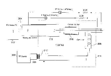
In Fig. 3, an RF source 300 and an microwave source 302
(e.g. power amplifier) are connected to deliver RF energy and
microwave energy respectively to a feed structure. Similarly
to Fig. 2, the feed structure comprises an RF channel 306 for
the RF energy and a microwave channel 304 for the microwave
energy. The RF channel 306 and microwave channel 304
comprises physically separate pathways from their respective
CA 3060535 2019-10-29
t
24
sources. The pathways are joined at a combining circuit 308.
The RF channel 306 includes a voltage transformer 310, which
isolates the combining circuit 308 from the RF source 300.
The microwave channel 304 includes a waveguide isolator 312,
which isolates the combining circuit 308 from the microwave
source 302. Thus, both inner and outer conductors on the RF
channel 306 and the microwave channel 304 on the combining
circuit side of the transformer 310 and waveguide isolator
respectively are floating, as indicated in Fig. 3 by dotted
box 314.
The electrosurgical apparatus of the present invention is
preferably capable of generating an RF signal having a power
of 150 W or more. According to IEC 60601, a 150 W RF power
generator may allow 1% (i.e. 1.5 Wrms) of the maximum
delivered power in a 200 fl resistor least favourably connected
between RF output and ground. In the comparative example
shown in Fig. 3, 200 fl resistors were connected between the
isolated grounds (output side and generator side) and between
the isolated RF output (output side) and isolated ground
(generator side). The power dissipated in these resistors was
measured using an oscilloscope. The power dissipated in the
200 fl resistor connected between the RF output and isolated
ground (generator side) was 4.7 Wrms, which is greater the
prescribed IEC 60601 minimum.
In one embodiment, the present invention provides a
coaxial isolator connected in line with the waveguide
isolator, i.e. in series between the waveguide isolator and
the combining circuit. The coaxial isolator consists of a
length of coaxial line with a series capacitor in the outer
conductor. Any example of a suitable coaxial isolator 500 is
shown in Figs. 7 and 8. The coaxial isolator 500 comprises an
input coaxial connector 502, which may be a Type N male
connector, and an output coaxial connector 504, which may be a
Type N female connector arranged opposite one another with a
space therebetween.
CA 3060535 2019-10-29
'
As shown in more detail in Fig. 8, the inner conductor
503 of the input connector 502 and the inner conductor 505 of
the output connector 504 each have a conductive sleeve 507,
509 mounted on their free ends. The conductive sleeve 507 of
5 the input connector 502 defines a first cooperating part (here
a recess). The conductive sleeve 509 of the output connector
504 defines a second cooperating part (here a projection)
which mates with the first cooperating part. The first and
second cooperating parts are separated from each other by an
10 insulating layer 511 (e.g. of Kapton tape). The insulating
layer may have a thickness of 0.3 mm or more.
Similarly, the outer conductor 513 of the input connector
502 and the outer conductor 515 of the output connector 504
each have a conductive sleeve 517, 519 mounted on their free
15 ends. The conductive sleeves 517, 519 mate with one another.
The conductive sleeves 517, 519 are separated from one another
by a insulating layer 518 (e.g. of Kapton tape), and a rigid
insulating spacer element 510 (e.g. of Delrin@).
The effect of the coaxial isolator is illustrated in Fig.
20 4, which shows an isolating circuit that is an embodiment of
the invention having a coaxial isolator 316 connected between
the waveguide isolator 312 and the combining circuit 308. The
other components of the circuit correspond to those in Fig. 3
and are given the same reference numbers. For this
25 arrangement, the power dissipated in a 200 n resistor
connected across the RF output and isolated ground (generator
side) is 1.47 Wrms, which meets the requirements of IEC 60601.
The coaxial isolator thus provides for improved patient
protection when the RF source is energised. Integrating the
waveguide isolator and coaxial isolator in a single
arrangement can assist in minimising microwave transmission
losses.
Fig. 9 is a schematic diagram showing another embodiment
of an isolating circuit for an electrosurgical apparatus.
Features in common with the embodiment of Fig. 2 are given the
CA 3060535 2019-10-29
26
same reference numbers and are not described again. In this
embodiment, the isolating circuit comprises a waveguide
isolator 600 whose insulating gap is configured to provide the
necessary level of DC isolation whilst also having an
capacitive reactance that is high enough at the frequency of
the RF energy to prevent coupling of RF energy across the
insulating gap and low enough at the frequency of the
microwave energy to prevent leakage of the microwave energy at
the gap. The configuration of the gap is explained in detail
with reference to Fig. 10. This configuration means that the
coaxial isolator used in the embodiment of Fig. 2 is not
needed.
In addition, in this embodiment the combining circuit is
integrated with the waveguide isolator 600. The signal
conductor 212 and ground conductor 214 carrying the RF signal
are connected to a coaxial RF connector 602, which introduces
the RF signal into the waveguide isolator 600, from where it
is conveyed out from the output port 232 towards the probe.
The isolating gap 603 is arranged to prevent the RF signal
from coupling back into the input port 230. Microwave energy
is prevented from coupling into the RF connector 602 by
careful placement of the inner conductive rod within the
waveguide isolator, as explained below. Combining the RF and
microwave energy in the waveguide isolator obviates the need
of a separate combining circuit, which reduces the number of
components required for the isolating circuit and enables it
to be provided as a more compact unit.
Fig. 10 shows a cross-sectional side view of the adapted
waveguide isolator 600 used in the isolating circuit of Fig.
9. Similarly to Fig. 5, the waveguide isolator 600 has a
cylindrical body made up of two mating parts. In this
embodiment, an input section 604 is a female component having
an opening for receiving an output section 606, which has a
cooperating male component. An input port 230 and an output
CA 3060535 2019-10-29
27
port 232 are mounted on the input section 604 and output
section 606 respectively in the same way as Fig. 5.
The DC gap, which insulates the input section 604 from
the output section 606 comprises a number of component parts.
The component parts all have rotational symmetry around the
axis of the cylindrical body. A first component part is a
primary insulating ring 608, e.g. made of rigid material such
as Delrin0 plastic, which surrounds the male component of the
output section 606 and separates (and electrically isolates)
the outer surfaces of the input section 604 and output section
606.
The axial length of the insulating ring 608 is shorter
than the male component of the output section 606, so that a
length of the male component extends beyond the distal end of
the insulating ring 608. This section of the male component
overlaps with the distal end of the female component of the
input section 604. A second component part of the DC gap is a
secondary insulating ring 612 (which may be formed in one
piece with the primary insulating ring 608) which provide a
radial insulation between the distal ends of the male and
female components.
A third component part of the DC gap is an insulating
film 610 (e.g. one or more layers of Kapton tape) which cover
the inside surface of the input section 604 for an axial
length beyond the distal end of the output section 606. The
insulating film can isolate the input section from any
fringing fields at the distal end of the output section 606.
A fourth component part of the DC gap is an air-filled
microwave choke 614, which is a narrow annular channel in the
distal end of the input section 604. The presence of the
microwave choke 614 lowers the capacitive reactance at the
frequency of the microwave energy, which prevents leakage
(e.g. radiation) of the microwave energy at the DC gap.
The increased complexity of the DC gap configuration in
this embodiment increases the capacitive reactance at the
CA 3060535 2019-10-29
28
frequency of the RF energy by widening the 'average' gap
between the input and output sections. Meanwhile the presence
of the microwave choke 614 makes use of resonant effects to
ensure that the capacitive reactance at the frequency of the
microwave energy is low enough to avoidance leakage of
microwave energy from the gap.
In this embodiment, the waveguide isolator also acts as
the combining circuit. The RF connector 602 has an inner
conductive rod 616 that projects into the waveguide isolator,
where it meets the inner conductor 618 of the coaxial output
probe (output port 232) at a point spaced from the end of the
inner conductor 618. Moreover, the position of the inner
conductive rod is selected to lie substantially parallel to
the equipotentials of the microwave energy in the waveguide
isolator so that it does not couple any significant microwave
power. This position can be determined by known simulation
techniques, and may be finely tuned permitting adjustment of
the radial position of the insertion point, or with a suitable
tuning screw.
CA 3060535 2019-10-29