Note: Descriptions are shown in the official language in which they were submitted.
1
MICROBOLOMETER DETECTORS AND ARRAYS FOR PRINTED PHOTONICS
APPLICATIONS
TECHNICAL FIELD
[0001] The technical field generally relates to microbolometers, and more
particularly, to
microbolometer detectors and arrays fabricated using printing techniques,
particularly ink-
based printing techniques.
BACKGROUND
[0002] Thermal detectors are devices that absorb energy from incident
electromagnetic
radiation and convert the absorption-generated heat into an electrical signal
indicative of
.. the amount of absorbed radiation. Perhaps the most prominent thermal
detectors currently
available are uncooled microbolometer detectors or, simply, microbolometers. A
microbolometer typically includes a suspended platform or bridge structure
having a low
thermal mass, which is held above and thermally insulated from a substrate by
a support
structure. The platform is provided with a thermistor, which is a resistive
element whose
electrical resistance changes in response to temperature variations caused by
the
absorbed radiation. The thermistor may, for example, be composed of a material
having
a high temperature coefficient of resistance (TCR), such as vanadium oxide and
amorphous silicon. Because they do not require cryogenic cooling, uncooled
microbolometers can operate at room temperature. This makes them well suited
for
integration within compact and robust devices that are often less expensive
and more
reliable than those based on cooled detectors. Other advantages of uncooled
microbolometers include reduced power consumption, smaller size, and reduced
weight.
Uncooled microbolometers can be used in various civilian and military
applications, in
fields such as defense and security, aerospace and astronomy, inspection and
maintenance, night vision, transportation, pollution and fire detection,
spectroscopy, and
remote sensing.
[0003] Arrays of uncooled microbolometers can be fabricated on a substrate
using
cornmon integrated-circuit-based microfabrication techniques, such as
photolithography
and surface micromachining. In such techniques, microbolometer components are
successively deposited and patterned on a substrate using thin-film deposition
techniques
paired with selective photoresist and sacrificial layer etching processes. In
some
applications, microbolometer detectors can be fabricated using a monolithic
integration
Date Recue/Date Received 2023-03-16
2
approach in which the substrate, typically provided with an underlying readout
integrated
circuit (ROIC), is pre-manufactured using complementary metal-oxide-
semiconductor
(CMOS) processes. Uncooled microbolometer arrays are often referred to as
"focal plane
arrays" (FPAs), while the individual microbolometer detectors forming the
arrays can be
referred to as "microbolometer pixels" or, simply, "pixels".
[0004] In most current applications, uncooled microbolometers are used to
sense
radiation in the infrared region of the electromagnetic spectrum, usually in
the mid-
wavelength infrared, encompassing wavelengths ranging from about 3 to about 5
micrometers (pm), or in the long-wave infrared, encompassing wavelengths
ranging from
about 8 to about 15 pm. These arrays are often integrated in uncooled thermal
cameras
for sensing infrared radiation emanating from an observable scene. Each
microbolometer
pixel absorbs some infrared radiation resulting in a corresponding change in
the pixel
temperature, which in turn produces a corresponding change in electrical
resistance of the
thermistor. A two-dimensional pixelated thermal image representative of the
infrared
radiation received from the scene can be generated by converting the changes
in electrical
resistance of each pixel into an electrical signal that can be displayed on a
screen or stored
for later viewing or processing. More recently, work and research have been
carried out
to extend the spectral range of operation of uncooled microbolometers beyond
the
traditional infrared range, notably in the far-infrared and terahertz (or sub-
millimeter)
spectral regions.
[0005] While conventional uncooled microbolometer detectors fabricated using
integrated-circuit-based techniques based on photolithography have advantages,
they
also have certain drawbacks and limitations. Examples of such drawbacks and
limitations
include small surface area coverage, relatively high cost, high processing
temperature,
high material consumption, limited fabrication flexibility, complex processing
procedures,
and limited compatibility with organic materials. Challenges therefore remain
in the
manufacturing of microbolometer detectors.
SUMMARY
[0006] The present description generally relates to microbolometer detectors
and arrays
fabricated using printed techniques, including ink-based printing technology,
such as, for
example, inkjet printing, aerosol jet printing, screen printing, and roll-to-
roll printing.
Date Recue/Date Received 2023-03-16
3
[0007] In accordance with an aspect, there is provided a microbolometer
detector
including a substrate, a platform suspended above the substrate, and a
thermistor printed
on the platform and made of a thermistor material that includes an
electrically conducting
polymer.
.. [0008] Depending on the application, the substrate and the platform can
each be made of
a flexible material, for example a polymer-based flexible material, a semi-
flexible material,
or a rigid material.
[0009] In one embodiment, the electrically conducting polymer of the
thermistor can
include poly(3,4-ethylenedioxythiophene) (PEDOT). In one variant, the
thermistor material
can include a functionalized PEDOT or a PEDOT-based copolymer. In some
embodiments, the functionalized PEDOT can be PEDOT functionalized with
substituents
to improve the dispersibility of the PEDOT in the solvent that is used to
prepare the ink
formulation applied for the fabrication of the thermistor. For example, the
PEDOT can be
functionalized with substituents such as alkyl, alkoxy, alkyl sulfonate
groups, and
combinations thereof.
[0010] In one embodiment, the thermistor material can be a PEDOT-based
copolymer,
such as poly(3,4-ethylenedioxythiophene) polystyrene sulfonate (PEDOT:PSS). In
other
embodiments, the PEDOT-based copolymer can include PEDOT or PEDOT:PSS, which
can be further modified with tetramethacrylate (TMA) or polyethylene glycol
(PEG) groups.
In one embodiment, the PEDOT can be dispersed in various solvents, such as,
for
example, toluene, dimethyl sulfoxide (DMSO), and water, with various
concentrations and
solids contents. The PSS concentration can be adjusted to provide the
PEDOT:PSS
copolymer with certain characteristics, for example to optimize or improve the
TCR of the
thermistor.
[0011] In one embodiment, the microbolometer detector includes an electrode
structure
printed on the platform and electrically connected to the thermistor. The
electrode structure
can be made of an electrode material that includes silver, copper, gold,
aluminum, carbon,
a metal composite, an electrically conducting metal oxide, or any combination
thereof,
which can be printed using an ink formulation based on nanoparlicles,
nanorods,
.. nanowires, nanotubes, and/or micro-pellets of these metals, metal
composites or metal
oxides.
Date Recue/Date Received 2023-03-16
4
[0012] In one embodiment, the microbolometer detector includes an ohmic
contact layer
interposed and forming an ohmic contact between the thermistor and the
electrode
structure. The ohmic contact layer can be made of an ohmic contact material
including an
electrically conducting polymeric composition selected to ensure or promote
structural and
electrochemical compatibility between the thermistor material and the
electrode material.
In one variant, the ohmic contact layer can be made of an ohmic contact
material that
includes a PEDOT-based polymeric composition, for example PEDOT and a carbon-
based nanomaterial, such as carbon nanotubes (CNTs). For example, in one
embodiment,
the thermistor material can include PEDOT:PSS, the electrode material can
include silver,
and the ohmic contact material can include a composition of PEDOT and CNTs.
[0013] In one embodiment, the microbolometer detector includes a passivation
layer
disposed over the thermistor.
[0014] In one embodiment, the microbolometer detector includes an optical
absorber
disposed over and in thermal contact with the thermistor. The optical absorber
is
configured to absorb electromagnetic radiation incident thereonto and convert
the
absorbed radiation into heat. The heat thus generated is transmitted to the
thermistor,
increases its temperature, and produces a corresponding change in its
electrical
resistance which can be measured to convey information about the amount of
absorbed
radiation energy.
[0015] In one embodiment, the microbolometer detector includes an
encapsulating
structure formed on the platform and defining a cavity encapsulating the
thermistor. The
encapsulating structure can include a cap supported above the platform in a
spaced
relationship therewith, and a spacer supporting the cap. In one variant, the
encapsulating
structure can further include an optical lens, for example mounted to the cap,
and
configured to focus electromagnetic radiation incident thereon onto the
platform.
[0016] In accordance with another aspect, there is provided a microbolometer
detector
including a flexible substrate; a platform suspended above the flexible
substrate; a
thermistor printed on the platform and made of a thermistor material including
a poly(3,4-
ethylenedioxythiophene) polystyrene sulfonate (PEDOT:PSS) polymeric
composition; an
electrode structure printed on the platform, the electrode structure being
electrically
connected to the thermistor and made of an electrode material including
silver; and an
Date Recue/Date Received 2023-03-16
5
ohmic contact layer interposed between the thermistor and the electrode
structure and
made of an ohmic contact material including a PEDOT-carbon nanotube polymeric
composition.
[0017] In accordance with another aspect, there is provided a microbolometer
array
including a plurality of arrayed microbolometer detectors, such as described
above.
Depending on the application, the microbolometer detectors can be arranged to
form a
linear or a two-dimensional matrix.
[0018] In accordance with another aspect, there is provided a printing method
for
fabricating a microbolometer detector or an array of such detectors, such as
disclosed
herein, the detectors including a suspended platform having an electrically-
conducting-
polymer-based thermistor printed thereon.
[0019] In accordance with another aspect, there is provided a microbolometer
detector,
including:
a substrate;
a platform suspended above the substrate;
a thermistor printed on the platform and made of a thermistor material
including an
electrically conducting polymer;
an electrode structure printed on the platform and electrically connected to
the
thermistor; and
an ohmic contact layer interposed between the thermistor and the electrode
structure,
wherein the ohmic contact layer is made of an ohmic contact material including
an electrically conducting polymeric composition.
[0020] In accordance with another aspect, there is provided a microbolometer
detector,
including:
a substrate;
a platform suspended above the substrate;
a thermistor printed on the platform and made of a thermistor material
including an
electrically conducting polymer; and
an encapsulating structure formed on the platform and defining a cavity
encapsulating
the thermistor.
Date Recue/Date Received 2023-03-16
6
[0021] In accordance with another aspect, there is provided a microbolometer
detector,
including:
a substrate;
a platform suspended above the substrate; and
a thermistor printed on the platform and made of a thermistor material
including an
electrically conducting polymer,
wherein the substrate, the platform, or both the substrate and the platform
are made
of a flexible material.
[0022] In some implementations, the present techniques relate to the design
and
.. fabrication of uncooled infrared microbolometer detectors and detector
arrays using
printing techniques on flexible substrates, such as inkjet printing or aerosol
jet printing. For
example, the present techniques can relate to the pixel array structure design
and related
fabrication materials and processes of the printed microbolometers, including
their
encapsulation, passivation, and thermal isolation. The present techniques are
not limited
.. to mid-wavelength infrared detection but can also be used in applications
in other infrared
spectral regions or in the terahertz region. The present techniques can also
be applied to
the design of printed microbolometer detectors for detection at specific
frequencies or in
specific frequency bands using frequency-selective absorbers. In some
implementations,
the manufacturing method can also be adapted for printing on rigid or semi-
rigid
.. substrates, such as glass, silicon wafers, or printed circuit board
substrates.
[0023] It is to be noted that other method and process steps may be performed
prior to,
during or after the method and process steps described herein. The order of
one or more
of the steps may also differ, and some of the steps may be omitted, repeated,
and/or
combined, depending on the application.
.. [0024] Other features and advantages of the present description will become
more
apparent upon reading of the following non-restrictive description of specific
embodiments
thereof, given by way of example only with reference to the appended drawings.
Although
specific features described in the above summary and the foregoing detailed
description
may be described with respect to specific embodiments or aspects, it should be
noted that
.. these specific features can be combined with one another unless stated
otherwise.
Date Recue/Date Received 2023-03-16
7
BRIEF DESCRIPTION OF THE DRAWINGS
[0025] Fig. 1A is a schematic cross-sectional elevation view of a
microbolometer detector,
in accordance with a possible embodiment. Fig. 1B is a schematic top plan view
of the
microbolometer detector of Fig. 1A, in which the optical absorber layer and
the passivation
layer have been removed to better illustrate the configuration of the
underlying
components.
[0026] Figs. 2A to 2H illustrate steps of a printing process to fabricate the
microbolometer
detector of Figs. 1A and 1B.
[0027] Fig. 3 is a schematic cross-sectional elevation view of a
microbolometer detector,
in accordance with another possible embodiment.
[0028] Fig. 4 is a schematic cross-sectional elevation view of a
microbolometer detector,
in accordance with another possible embodiment.
[0029] Fig. 5A is a schematic cross-sectional elevation view of a
microbolometer array
including a plurality of microbolometer detectors arranged in a two-
dimensional matrix of
rows and columns, in accordance with a possible embodiment. Fig. 5B is a
schematic top
plan view of the microbolometer array of Fig. 5A. In Fig. 5B, the optical
absorber layer and
the passivation layer of each microbolometer detector have been removed to
better
illustrate the configuration of the underlying components.
[0030] Figs. 6A to 6C are schematic cross-sectional elevation views of
microbolometer
arrays, in accordance with three other possible embodiments.
[0031] Figs. 7A to 7D illustrate a printing method for fabricating PEDOT:PSS-
based
thermistors on a flexible substrate.
[0032] Fig. 8A is a schematic representation of a 6 x 10 array of
microbolometer detectors
including PEDOT:PSS thermistors, a passivation layer, and silver-based
electrical
interconnections, printed on a flexible polyimide (PI) substrate using the
present
techniques. Fig. 8B is a schematic representation of an 8x16 array of
microbolometer
detectors including multiplexed PEDOT:PSS thermistors printed on a flexible PI
substrate
using the present techniques.
Date Recue/Date Received 2023-03-16
8
[0033] Fig. 9 depicts temperature-dependent electrical resistance measurements
performed on an array of PEDOT:PSS-based microbolometer detectors
corresponding to
the one depicted in Fig. 8A. Each curve in Fig. 9 depicts the resistance of
the PEDOT:PSS
thin-film thermistor measured on a different detector of the microbolometer
array as a
function of the detector temperature and under a bias current of 10 pA.
[0034] Fig. 10 is a graph showing curves of the terminal voltages of the
thermistors of two
different PEDOT:PSS-based microbolometer detectors, measured as functions of
the
temperature of a blackbody to which the detectors were exposed. The slope of
each curve
represents the responsivity of each microbolometer detector.
DETAILED DESCRIPTION
[0035] In the present description, similar features in the drawings have been
given similar
reference numerals. To avoid cluttering certain figures, some elements may not
be
indicated if they were already identified in a preceding figure. It should
also be understood
that the elements of the drawings are not necessarily depicted to scale, since
emphasis is
placed on clearly illustrating the elements and structures of the present
embodiments.
Furthermore, positional descriptors indicating the location and/or orientation
of one
element with respect to another element are used herein for ease and clarity
of description.
Unless otherwise indicated, these positional descriptors should be taken in
the context of
the figures and should not be considered limiting. As can be appreciated, such
spatially
relative terms are intended to encompass different orientations in the use or
operation of
the present embodiments, in addition to the orientations exemplified in the
figures.
[0036] In the present description, when a first element is referred to as
being "on", "above",
"below", "over", or "under" a second element, the first element can be either
directly or
indirectly on, above, below, over, or under the second element, respectively,
such that one
or multiple intervening elements may be disposed between the first element and
the
second element.
[0037] Unless stated otherwise, the terms "connected" and "coupled", and
derivatives and
variants thereof, are intended to refer to any connection or coupling, either
direct or
indirect, between two or more elements. For example, the connection or
coupling between
the elements may be mechanical, optical, electrical, thermal, chemical,
logical,
operational, or any combination thereof.
Date Recue/Date Received 2023-03-16
9
[0038] In the present description, the terms "a", "an", and "one" are defined
to mean "at
least one", that is, these terms do not exclude a plural number of elements,
unless stated
otherwise.
[0039] Terms such as "substantially", "generally", and "about", that modify a
value,
condition, or characteristic of a feature of an exemplary embodiment, should
be
understood to mean that the value, condition, or characteristic is defined
within tolerances
that are acceptable for the proper operation of this exemplary embodiment for
its intended
application or that fall within an acceptable range of experimental error. In
particular, the
term "about" generally refers to a range of numbers that one skilled in the
art would
consider equivalent to the stated value (e.g., having the same or equivalent
function or
result). In some instances, the term "about" means a variation of 10 percent
of the stated
value. It is noted that all numeric values used herein are assumed to be
modified by the
term "about", unless stated otherwise.
[0040] The present description generally relates to microbolometer detectors,
and more
particularly to microbolometer detectors and detector arrays fabricated using
printed
electronics techniques, and to related print-based fabrication methods.
[0041] In the present description, the term "microbolometer" is intended to
refer to a
thermal detector that operates by absorbing incident electromagnetic
radiation, converting
the absorbed radiation into heat, and sensing the resulting temperature
increase of the
detector through a change of the electrical resistance of a thermistor made of
a thermistor
material having a suitable TCR. The thermistor is generally thermally
insulated, such that
its temperature changes in response to the absorbed incident radiation but
remains mostly
unaffected by the temperature of its surroundings. Microbolometers can be
classified as
either cooled or uncooled, depending on whether their operation involves
cryogenic
cooling or not. It is also appreciated that, in the present description, the
terms
"microbolometer" and "bolometer" can generally be used interchangeably.
[0042] In the present description, the terms "light" and "optical", and
variants and
derivatives thereof, are intended to refer to radiation in any appropriate
region of the
electromagnetic spectrum. These terms are therefore not limited to visible
light, but can
also include, without being limited to, the infrared, terahertz and millimeter
wave regions.
For example, in some implementations, the present techniques can be used with
Date Recue/Date Received 2023-03-16
10
electromagnetic signals having wavelengths ranging from about 0.2 pm to about
3000 pm.
However, this range is provided for illustrative purposes only and some of the
present
techniques may operate outside this range. Infrared radiation is commonly
divided into
various spectral regions, which include the near-infrared (NIR) region for
wavelengths
ranging from 0.7 to 1.4 pm; the short-wavelength infrared (SWIR) region for
wavelengths
ranging from 1.4 to 3 pm; the mid-wavelength infrared (MWIR) region for
wavelengths
ranging from 3 to 8 pm; the long-wavelength infrared (LWIR) region for
wavelengths
ranging from 8 to 15 pm; and the far-infrared (FIR) region for wavelengths
ranging from
to 1000 pm. It is appreciated that the definitions of different infrared
regions in terms of
10 spectral ranges, as well as their limits, can vary depending on the
technical field under
consideration, and are not meant to limit the scope of application of the
present
techniques.
[0043] The microbolometer detectors and arrays disclosed herein can be
fabricated by
means of printed electronics and photonics techniques, particularly ink-based
printing
15 techniques.
[0044] In the present description, the terms "printed electronics" and
"printed photonics"
refer to a set of printing technologies used to create electronic and photonic
structures on
various substrates. The term "printed" refers in this context to various
additive, non-
contact, and/or maskless patterning and manufacturing techniques capable of
producing
electronic and photonic devices and systems from the printed matter. Examples
of printing
techniques include, but are not limited to, inkjet printing, aerosol jet
printing, screen
printing, roll-to-roll printing, intaglio printing, flexographic printing,
offset printing, stamp
printing, and gravure printing. Compared to conventional integrated-circuit-
based
techniques involving subtractive processes, such as photolithography and
etching,
additive printing processes offer a number of advantages for developing
alternative
bolometer devices. Such advantages include simplicity, lower cost, lower
processing
temperatures, reduced material waste, scalability to large coverage areas, and
compatibility with flexible plastic and other organic substrates.
[0045] Inkjet printing is a promising additive manufacturing technique used
for fabricating
flexible electronic devices in various fields and applications, including the
semiconductor,
chemical, biological, biomedical, and pharmaceutical industries. Inkjet
printing is usually
classified as either continuous inkjet printing or drop-on-demand (DOD)
printing. Inkjet
Date Recue/Date Received 2023-03-16
11
printing is capable of printing features with linewidth as small as 1 pm to
allow production
miniaturization. Inkjet printing can offer low-cost and low-temperature
selective printing on
large-area flexible substrates, which may not be easily achievable with
standard
photolithography. Inkjet printing processes can be digitally controlled by a
computer, thus
avoiding the use of masks or screens, while enabling simpler and faster device
manufacturing and customization. With a typical distance between the substrate
and the
inkjet printer head of just one millimeter (mm), inkjet printing is a non-
contact deposition
and patterning technique. The non-contact nature of inkjet printing reduces
the risk of
causing damage to fragile substrates and makes it possible to use inkjet
printing for
material deposition on top of existing three-dimensional (3D) topologies and
inside
trenches and cavities, which can be a challenge for traditional contact
printing techniques,
such as screen printing and roll-to-roll printing. Industrial inkjet printers
have a large
number of parallel nozzles, and several print heads can be stacked into an
array to
improve throughput. By printing multiple layers of material one on top of the
other, inkjet
printing can also be used as a 3D printing method. Because inkjet printing
can, in principle,
be used with any digital layout, which can contain either fine patterns or
homogeneous
layers, it has the potential to be used to print a wide range of functional
materials.
[0046] The present techniques have potential use in various consumer,
industrial and
military applications that may benefit from or require printed microbolometer
detectors
produced at low cost on large-area flexible substrates. Non-limiting examples
of possible
fields of use include defense and security, medicine, industrial control,
robotics, sports and
entertainment, food supply chain management, and the Internet of Things. In
some
implementations, the present techniques can be used for detection of infrared
radiation
and contact and non-contact temperature sensing.
[0047] Various implementations of the present techniques are described below
with
reference to the figures.
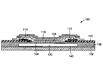
[0048] Referring to Figs. 1A and 1B, there are illustrated a schematic cross-
sectional
elevation view and a schematic top plan view, respectively, of a possible
embodiment of
an uncooled microbolometer detector 100. For example, the microbolometer
detector 100
of Fig. 1 can be used as one pixel of a microbolometer array of a thermal
camera or
imaging device. As such, the term "microbolometer detector" may, in some
instances, be
used interchangeably with the term "microbolometer pixel". The microbolometer
Date Recue/Date Received 2023-03-16
12
detector 100 is formed as a stack of layers printed on a substrate 102 and
includes a
suspended platform 104, a support structure 106, a thermistor 108, an
electrode
structure 110, an ohmic contact layer 112, a passivation layer 114, and an
optical
absorber 116. The structure, composition, and operation of these and other
possible
components of the microbolometer detector 100 will be described in greater
detail below.
It is noted that in Fig. 1B, the passivation layer and the optical absorber
have been omitted
to better illustrate the configuration of the underlying components, namely
the
thermistor 108, the electrode structure 110, and the ohmic contact layer 112.
[0049] Depending on the application, the microbolometer detector 100 can be
fabricated
either entirely or partially by printing technology. Non-limiting examples of
printing
techniques that may be used include inkjet printing, aerosol jet printing,
screen printing,
and roll-to-roll printing. Figs. 2A to 2H illustrate possible steps of a
printing process used
to fabricate a microbolometer detector 100, such as the one of Figs. 1A and
1B.
[0050] Returning to Figs. 1A and 1B, the substrate 102 provides a structure
that physically
holds and supports the other components of the microbolometer detector 100. In
some
implementations, the substrate 102 can be made of a flexible material. The
flexible
material can be a polymer material, such as, for example, polyethylene
terephthalate
(PET), polyethylene naphthalate (PEN), polypropylene (PP), polyimide (PI), or
polycarbonate (PC). Non-limiting examples of advantages of providing a
microbolometer
detector or array on a flexible substrate include a compatibility with uneven
surfaces or
structures, a compatibility with large area coverage, and the possibility of
forming
microbolometer arrays that can be folded, rolled, and/or stretched. In other
implementations, however, the substrate 102 can be a semi-flexible or a rigid
substrate,
which can be made, for example, from fused silica, quartz, silicon, or
fiberglass.
[0051] Depending on the application, the substrate 102 can be a single (Fig.
2A) or a
multilayered structure. In some implementations, the thickness of the
substrate can range
from about 5 pm to about 2000 pm, although other thickness values are possible
in other
implementations. In some embodiments, the printing process used can be
optimized in
accordance with the surface tension and/or morphology of the substrate 102.
The printing
of subsequent layers on the substrate 102 can involve various surface
treatments to
improve film adhesion and surface tension between the substrate 102 and the
Date Recue/Date Received 2023-03-16
13
subsequently printed layers. Depending on the application, such surface
treatments can
involve wet and/or dry chemical processes.
[0052] The microbolometer detector 100 also includes a platform 104 suspended
above
the substrate 102 by the support structure 106. In the present description,
the term
"platform" generally refers to a substantially planar suspended bridge or
membrane
structure, typically having greater horizontal dimensions than vertical
thickness. In the
present description, the term "horizontal" refers to directions lying in a
plane parallel to the
substrate 102, while the term "vertical" refers to a direction perpendicular
to the plane of
the substrate 102.
[0053] The suspension of the platform 104 above the substrate 102 can provide
thermal
isolation to the thermistor 108. By thermally insulating the thermistor 108,
the detection
sensitivity of the microbolometer detector 100 can be enhanced. The platform
104 may be
shaped as a substantially rectangular, single or multilayer structure, and be
made of an
electrically insulating, mechanically self-supportive, and low-stress
material. As for the
substrate 102, the platform 104 can be made of a flexible material, for
example with a
polymeric composition, a semi-flexible material, or a rigid material. Non-
limiting examples
of suitable materials that can be used to form the platform 104 include: SU-8
photoresist;
InkOrmo, a UV-curable hybrid polymer manufactured by micro resist technology
GmbH
(Berlin, Germany); polyvinylphenol (PVP); polydimethylsiloxane (PDMS);
polyimide (PI);
polyethylene terephthalate (PET); polycarbonate (PC); and various other
organic and
inorganic dielectric materials.
[0054] Depending on the type and thickness of the substrate 102, the platform
104 may
have lateral dimensions ranging between about 50 pm and about 10 mm and a
thickness
ranging between about 10 pm and 2 mm, although other dimensions can be used on
other
implementations. Depending on the application, the platform 104 can be formed
in a
variety of shapes, dimensions, and configurations, without departing from the
scope of the
present techniques. Furthermore, in some implementations, for example those
that do not
include an optical absorber layer, the platform 104 may be made of a material
that absorbs
and is heated by electromagnetic radiation in the operation spectral range of
the
microbolometer detector 100.
Date Recue/Date Received 2023-03-16
14
[0055] In the illustrated embodiment, the platform 104 is printed on top of a
sacrificial
layer 118 (see Fig. 2C). The sacrificial layer 118 can be formed on the
substrate 102
during the fabrication process of the microbolometer detector 100 (Fig. 2B)
and be
subsequently dissolved or otherwise removed to define a gap 120 between the
substrate 102 and the platform 104 (see Fig. 2G). In some implementations, the
sacrificial
layer 118 can be dissolved using a variety of solvents either in liquid or
vapor phase.
Depending on the device architecture and materials chemistry, plasma release
of the
sacrificial layer 118 may also be possible. Water-soluble polymers, such as
poly(vinyl
alcohol) (PVA), poly(acrylic acid) (PAA), polyethylene glycol (PEG),
polyvinylpyrrolidone,
and the like, can be used as the sacrificial layer 118 material. It is noted
that when the
platform 104 is made of a polymeric material, common removers in standard
microfabrication processes generally cannot be used to dissolve the
sacrificial layer 118.
[0056] In other implementations, such as in the case of thin substrates, for
example made
of PI, PET, or PC, laser trimming or other similar techniques that do not
involve the use of
a sacrificial layer may be used to form the platform 104 and achieve thermal
isolation of
the thermistor 108. Such a laser trimming process can be performed by using a
high-
repetition-rate ultrashort-pulse laser. The isolation of the detector can be
achieved by
directly trimming the edges of the detector. The cavity and detector
suspension can be
obtained by stacking multiple substrates using thermocompression bonding or a
lamination process. Thermocompression bonding or a lamination process can also
be
used for hermetic sealing of the pixel array, as described below.
[0057] In some implementations, a reflector 140 can be deposited on the
substrate 102
under the platform 104 (see also Fig. 2A). The reflector 140 may include a
thin metal film,
for example a thin aluminum, gold, or silver film. The reflector 140 may be a
continuous or
discontinuous film. The reflector 140 can form an optical resonant cavity with
the
platform 104 separated therefrom by the gap 120, which can enhance the optical
absorption properties of the microbolometer detector 100. Depending on the
application,
the reflector 140 can be formed by printing techniques or other deposition
techniques, for
example vacuum evaporation.
[0058] Referring still to Figs. 1A and 1B, the platform 104 is held above the
substrate 102
by the support structure 106. In the present description, the term "support
structure" is
used to refer broadly to a structure configured to hold the platform 104 in a
spaced-apart
Date Recue/Date Received 2023-03-16
15
relationship above the substrate 102. In some implementations, the support
structure 106
can provide enough mechanical rigidity and strength to maintain the platform
104 at a
height ranging from about a few microns to a few hundreds of microns above the
substrate 102, although other height values are possible in other
implementations. The
support structure 106 can also provide a path for the electrode structure 110
that connects
the thermistor 108 to an ROIC (not shown). The ROIC, which can be an
electrical
multiplexing circuit, can be provided in the substrate 102 and include thin-
film transistor
(TFT)-based integrated circuits and other passive and/or active components. In
some
embodiments, the ROIC can be fabricated using a hybrid approach including both
printed
electronic devices and surface-mounted CMOS devices on a flexible substrate.
[0059] The support structure 106 may be provided as one or more printed thin-
film layers
and may be made of a low-stress and self-supporting material, such as those
listed above
for the substrate 102 and the platform 104. Depending on the application, the
support
structure 106 may or may not have the same composition as the platform 104.
The support
structure 106 is generally fabricated (e.g., printed) concurrently with the
platform 104.
[0060] The support structure 106 can extend along or close to the outer
periphery of the
platform 104. In the embodiment of Figs. 1A and 1B, the support structure 106
includes
two support beams located on two opposite sides of the platform 104, but other
configurations could be used in other embodiments, for example with four
support beams
provided on the four corners of the platform 104. In particular, the support
structure 106
can have a variety of configurations to meet the requirements or preferences
(e.g.,
structural, electrical, and/or thermal) of a given application. For example,
in some
implementations, the support structure 106 may extend closer to the center of
the
platform 104 rather than near its outer periphery.
[0061] In the embodiment of Figs. 1A and 1B, the microbolometer detector 100
includes
a thermistor 108 printed on the platform 104 (see also Fig. 2F). In the
present description,
the term "thermistor" generally refers to a thermally sensitive resistor made
of any suitable
material, structure or device having an electrical resistance that changes as
a function of
its temperature, generally in a predictable and controllable manner. The
thermistor 108
can be made of a material having a high TCR at room temperature, for example
at least
0.5% per kelvin. In the illustrated embodiment, the microbolometer detector
100 includes
a single thermistor 108 printed on the platform 104 as a rectangular thin film
whose width,
Date Recue/Date Received 2023-03-16
16
length, and thickness may be selected in order to control its electrical
resistance. As can
be appreciated, the size, shape, and arrangement of the thermistor 108 may be
varied
depending on the application. In some embodiments, the microbolometer detector
100
can include two or more thermistors 108 printed on the platform 104.
.. [0062] The thermistor 108 can be made of a thermistor material composed of
an
electrically conducting polymer, for example a semiconducting polymer,
compatible with
print-based deposition and patterning technologies.
[0063] In some embodiments, the electrically conducting polymer can include
poly(3,4-
ethylenedioxythiophene) (PEDOT). PEDOT is a flexible, electrically conducting
.. conjugated polymer that is optically transparent in the visible region.
PEDOT is generally
a low molecular weight polymer that can present low solubility in some
solvents. Therefore,
in some embodiments, PEDOT can be modified and/or functionalized to increase
its
dispersibility or solubility. Thus, in some embodiments, the conducting
polymer can
include PEDOT functionalized with substituents to improve dispersibility of
PEDOT in the
solvent that is used to prepare the ink composition applied for the
fabrication of the
thermistor. For example, PEDOT can be functionalized with substituents
including alkyl,
alkoxy, and/or alkyl sulfonate groups, to name a few.
[0064] In other embodiments, the conducting polymer can include a PEDOT-based
copolymer, such as poly(3,4-ethylenedioxythiophene) polystyrene sulfonate
(PEDOT:PSS). PSS is an electrically insulating polymer, generally of a high
molecular
weight, which can provide flexibility and increased solubility in water and/or
other solvents,
resulting in improved processability. In a PEDOT:PSS copolymeric structure,
the PEDOT
segments are electrostatically attached to the PSS polymer chains. The PEDOT
to PSS
molar and weight ratios can be varied depending on the application. The
balancing
between the optoelectronic properties of PEDOT:PSS co-polymers, with their
structure
and the ratio between their electrically conducting part (PEDOT) and their
electrically
insulating part (PSS), can make them good transparent printable thermistor
materials. In
some variants, PSS can be replaced or combined with other oligomeric or
polymeric
segments including, for example, tetramethacrylate (TMA) or polyethylene
glycol (PEG).
The use of PEDOT:PSS formulations as thermistor material can be advantageous
since
PEDOT:PSS is available at low cost, optically transparent to visible light,
mechanically
flexible, thermally stable, and easily processable.
Date Recue/Date Received 2023-03-16
17
[0065] Thermistor films of PEDOT:PSS can be deposited by inkjet printing or
other ink-
based printing techniques by using suitable PEDOT:PSS-based ink formulations.
Various
types of PEDOT:PSS-based ink formulations can be used including, but not
limited to,
solutions, emulsions, and dispersions. The ink formulations can be chemically
optimized
or adjusted by changing the PSS concentration and/or the pH of the dispersion
to improve
the TCR and/or the sheet resistance of the PEDOT:PSS thermistor to be printed.
In some
implementations, a PEDOT:PSS thermistor having a TCR ranging from about 0.5%/K
to
about 10%/K can be obtained.
[0066] In some implementations, the PEDOT:PSS copolymer can be
dispersed/dissolved
in a mixture of one or more solvents, such as water and/or organic solvents,
to obtain
PEDOT:PSS-based ink formulations. Non-limiting examples of organic solvents
that can
be used to disperse/dissolve PEDOT:PSS include toluene, DMSO, ethylene glycol,
and
the like. In some implementations, the PEDOT:PSS-based ink formulations can
include
some additives, if required or desired, to further improve their
processability and/or
enhance the thermistor material properties. Non-limiting examples of possible
additives
include surfactants, electrical conductivity enhancers, dopants, stabilizers,
and the like.
[0067] Referring still to Figs. 1A and 1B, the microbolometer detector 100
includes an
electrode structure or layer 110 configured to provide an electrical
connection between
the thermistor 108 and the ROIC (e.g., an electrical multiplexing circuit) and
other
electronics (not shown). The ROIC can be active or passive and be configured
to measure
changes in the electrical resistance of the thermistor 108 caused by heating
resulting from
the absorption of electromagnetic radiation.
[0068] The electrode structure 110 may be deposited and patterned on the
platform 104
using various printing techniques, such as those mentioned above (see also
Fig. 2D). The
electrode structure 110 may be made of any printable material having a
suitable electrical
conductivity. Depending on the application, the shape, size, and configuration
of the
electrode structure 110 may be adjusted to control its electrical and/or
thermal properties
and, in turn, enhance the performance of the microbolometer detector 100. For
example,
in the embodiment of Figs. 1A and 1B, the electrode structure 110 is connected
to the
thermistor 108 at two opposite ends thereof.
Date Recue/Date Received 2023-03-16
18
[0069] In some implementations, the electrode structure 110 can be printed by
inkjet or
aerosol jet printing using ink formulations based on metallic or other
electrically conducting
microstructures and nanostructures (e.g., nanoparticles, nanorods, nanowires,
nanotubes, and micro pellets) or other electrically conducting organic and
inorganic
polymers dispersed in a solvent. For example, the microstructures and
nanostructures can
be made of silver, copper, gold, aluminum, carbon, a metal composite (e.g.
polymer-metal
composite), and/or an electrically conducting metal oxide.
[0070] In some implementations, a thermal treatment and sintering process of
the printed
electrode structure 110 can be performed. The sintering temperature can be
selected
based on the nature of the substrate and the temperatures that can be
withstood by the
other printed materials forming the microbolometer detector 100. In some
applications,
such temperature constraints can put some limitations on the achievable sheet
resistance
of the electrode structure 110. In such a case, localized surface heating, for
example using
a pulsed laser source or another high-intensity pulsed light source can be
used to achieve
a required or desired sheet resistance, while avoiding or at least mitigating
thermal
diffusion and degradation of the substrate and other printed materials.
[0071] Referring still to Figs. 1A and 1B, the microbolometer detector 100
includes an
ohmic contact layer 112 printed and forming an ohmic contact between the
thermistor 108
and the electrode structure 110 (see also Fig. 2E). The ohmic contact layer
112 provides
a low-resistance electrical path between the thermistor 108 and the electrode
structure 110, for example less than one percent of the resistance of the
thermistor 108.
In addition to providing a low-resistance path for electrical current to flow
in and out of the
thermistor 108, the ohmic contact layer 112 can ensure or promote structural
and/or
chemical compatibility between the thermistor 108 and the electrode structure
110. The
composition of the ohmic contact layer 112 can be selected by considering the
compositions of both the thermistor material and the electrode material.
[0072] In some implementations, the ohmic contact layer 112 can be made of an
ohmic
contact material based on PEDOT, such as an ohmic contact material that
includes
PEDOT and a carbon-based nanomaterial. For example, the carbon-based
nanomaterial
can include carbon nanowires, graphene, carbon nanotubes (CNTs), fullerenes,
and a
combination thereof. The CNTs can be single-walled nanotubes (SWNTs) and/or
multi-
walled nanotubes (MWNTs). In some implementations, the ohmic contact material
can
Date Recue/Date Received 2023-03-16
19
include PEDOT and CNTs, wherein the ratios of PEDOT and CNTs can vary to
achieve a
required or desired dispersion of CNTs having a sufficiently high electrical
conductance,
while avoiding agglomeration in the dispersion. In some implementations, the
CNTs can
have a length ranging from about 50 nanometers (nm) to about 2 pm, and a
diameter of a
few nanometers. In some implementations, the PEDOT-CNT compound can be
dispersed/dissolved in a mixture of one or more solvents, such as water and/or
organic
solvents, to obtain PEDOT-CNT-based ink formulations. Non-limiting examples of
organic
solvents that can be used to disperse/dissolve PEDOT-CNT compounds include
toluene,
DMSO, ethylene glycol, and the like.
[0073] In some implementations, the thermistor material can include a
printable PEDOT-
based polymer and the ohmic contact layer can be made of an ohmic contact
material that
includes a printable PEDOT-based polymeric composition that is different from
the
PEDOT-based polymer used for the thermistor. The printable PEDOT-based
polymeric
composition used for the ohmic contact layer 112 can be selected in view of
its structural
and electrochemical compatibility with both the thermistor material and the
electrode
material. In one embodiment, the thermistor material can include PEDOT:PSS,
the
electrode material can include silver, and the ohmic contact material can
include a
printable composition of PEDOT-carbon nanotubes (PEDOT-CNT). In particular, it
has
been found that PEDOT-CNT can exhibit a good chemical compatibility with
PEDOT:PSS
and provide a low-resistance contact between PEDOT:PSS and a silver-based
electrode
structure.
[0074] Referring still to Figs. 1A and 1B, the microbolometer detector 100 can
further
include a passivation layer 114 printed on the thermistor 108. The passivation
layer 114
is configured to seal or cover the thermistor 108 and the ohmic contact layer
112 by
providing a barrier to the diffusion of water, oxygen and other impurities
that could
otherwise degrade or affect the performance of the microbolometer detector
100.
Depending on criteria such as the performance, reliability, and life
expectancy of the
microbolometer detector 100, the passivation layer 14 can be prepared by
various
techniques including, but not limited to, deep coating, inkjet printing,
aerosol jet printing,
spray coating, sputtering, and low temperature plasma chemical vapor
deposition. Non-
limiting examples of materials that can be used for passivation of printed
devices include
liquid glasses, metal oxides, silicon oxides, and silicon nitrides.
Date Recue/Date Received 2023-03-16
20
[0075] The microbolometer detector 100 can further include an optical absorber
116
printed or otherwise formed over and in thermal contact with the thermistor
108 (see also
Fig. 2H). The optical absorber 116 is configured to absorb electromagnetic
radiation
incident thereon and to convert the absorbed radiation into heat. The heat
thus generated
is transmitted to the thermistor 108, increases its temperature, and produces
a
corresponding change in its electrical resistance that can be measured to
convey
information about the intensity of the incident radiation. The provision of
the optical
absorber 116 can enhance the sensitivity and overall performance of the
microbolometer
detector 100, for example in near-infrared and far-infrared applications. As
noted above,
.. the term "optical" refers to electromagnetic radiation in general and is
not limited to the
visible or another portion of the electromagnetic spectrum. It is noted that
some
embodiments may not include a dedicated optical absorber layer, such as those
illustrated
in Figs. 3 and 4.
[0076] In the present description, the term "thermal contact" generally means
that heat
.. conduction occurs directly or indirectly between two elements, that is, the
two elements
may be in direct contact with each other or may have a sufficiently thermally
conducting
material present between them. Specifically, the term "thermal contact" is
intended to refer
to the fact that when the optical absorber 116 is heated upon absorption of
electromagnetic radiation, the heat thus generated is conducted, radiated or
otherwise
transmitted to the thermistor 108, for example through the passivation layer
114.
[0077] The optical absorber 116 can be formed by printing ink formulations
containing
carbon-based materials, such as carbon nanowires, graphene, CNTs, fullerenes,
and the
like. The thickness of the optical absorber 116 can be selected to tailor its
absorption
spectrum. It is appreciated, however, that other deposition techniques, for
example spray
coating and vacuum evaporation, may be considered to deposit a carbon-based
optical
absorber layer. The choice of a particular deposition technique can be
dictated by the
thickness of the film to be formed, its uniformity, and the processing
temperature. Another
approach to enhance the sensitivity of the microbolometer detector 100 and
tailor its
absorption spectrum is to provide the optical absorber 116 as a frequency
selective
structure obtained by inkjet printing using different high-electrical-
conductivity metallic
nanoparticle formulations, such as silver, gold, aluminum, and copper. In
other
implementations, other suitable materials for the optical absorber 116 can
include, without
Date Recue/Date Received 2023-03-16
21
being limited to, metal black, such as gold black, organic black, graphene,
carbon
nanotubes, chromium, nickel-chromium, vanadium, titanium, and titanium-
nitride.
[0078] Referring to Fig. 3, there is illustrated another embodiment of a
microbolometer
detector 100. The microbolometer detector 100 generally includes a substrate
102, a
suspended platform 104, a support structure 106, a thermistor 108, an
electrode
structure 110, an ohmic contact layer 112, a passivation layer 114, and a
reflector 140. An
optical absorber such as shown in Fig. 1A could optionally be provided,
depending on the
application. These features can be generally similar to like features
described above with
respect to the embodiment of Figs. 1A and 1B, and they will not be described
again in
detail.
[0079] The microbolometer detector 100 of Fig. 3 further includes an
encapsulating
structure 122 formed on top of the platform 104 and defining a sealed cavity
124
encapsulating the thermistor 108 and preventing performance degradation caused
by
diffusion of water, oxygen, and other foreign matter. Depending on the
application, the
cavity 124 may be under vacuum or filled with a gas having a low thermal
conductivity,
such as krypton, xenon, and argon. Encapsulation of the microbolometer
detector 100 in
a hermetic package architecture can be provided to achieve high sensitivity to
electromagnetic radiation, stable performance, and long-term reliability. In
Fig. 3, the
encapsulating structure 122 can include a cap 126 supported above the platform
104 in a
spaced relationship therewith and a spacer 128 supporting the cap 126 and
defining the
depth of the hermetically sealed cavity 124. The cap 126 and the spacer 128
can be
formed using various approaches. In one embodiment, the spacer 128 may be
fabricated
by jet printing or laser trimming, depending on the height of the cavity 124.
The spacer 128
may be made of the same type of material as the passivation layer 114 to
improve the
sealing of the cavity 124. The cap 126 can be configured to provide a required
or desired
optical transmittance in the spectral band of interest. In the illustrated
embodiment, the
cap 126 includes a cap substrate 130 and a cap passivation layer 132 formed on
the cap
substrate 130. For example, the cap substrate 130 can be made of a thin film
of polyimide
or polyethylene, and the cap passivation layer 132 can be made of the same
material as
the spacer 128. The encapsulating structure 122 can be formed by turning the
cap 126
upside down and placing it on top of the spacer 128, such that the cap
passivation
layer 132 is brought in contact with and adhered to the spacer 128. Non-
limiting examples
of the processes which can be used to encapsulate the microbolometer detector
100
Date Recue/Date Received 2023-03-16
22
include multilayer film lamination, adhesive bonding, metal to metal
thermocompression
bonding, and laser sealing. The choice of a particular process can be dictated
by the
processing temperature and the properties of the materials forming the
encapsulating
structure 122.
[0080] Referring to Fig. 4, there is illustrated another possible embodiment
of a
microbolometer detector 100 that incorporates focusing optics to collect and
focus incident
electromagnetic radiation. As in the embodiment of Fig. 3, the microbolometer
detector 100 of Fig. 4 includes an encapsulating structure 122 including a cap
126 and a
spacer 128 defining the hermetically sealed cavity 124. The encapsulating
structure 122
further includes an optical lens or focusing optics 134 formed on or in the
cap 126 and
configured to focus electromagnetic radiation incident thereon onto the
underlying
platform 104. In the illustrated embodiment, the optical lens 134 forms a
biconvex lens
made of an outer convex lens portion 136 formed on the cap substrate 130 and
facing
away from the underlying platform 104, and an inner convex lens portion 138
formed on
the cap passivation layer 132 and facing toward the underlying platform 104.
[0081] In some embodiments, non-printing micro-assembly techniques can be used
to
directly assemble the optical lens 134 on the cap 126, for example with the
aid of an
automated high-precision alignment system. For instance, crystalline lenses
made of
germanium or zinc selenide may be used in near-infrared and mid-wavelength
infrared
applications, while high-resistivity silicon may be used in far-infrared
applications. As can
be appreciated, other lens materials can be used in other implementations. In
other
embodiments, the optical lens 134 can be fabricated by inkjet or aerosol jet
printing, for
example using nanoparticle-based or polymer-based ink formulations. The
optical
properties of the lens 134 can be adjusted via the chemical composition of the
particular
ink formulation and the sintering temperature. Furthermore, the radius of
curvature and
the focal length of the optical lens 134 can be tailored by adjusting the
viscosity of the ink
formulation, the surface tensions between the lens 134 and the cap 126, and
the types of
solvents used in the ink formulations.
[0082] Referring now to Figs. 5A and 5B, there is illustrated a microbolometer
array 200
that includes a plurality of microbolometer detectors or pixels 100, such as
described
above, arranged in a two-dimensional matrix of rows and columns. In some
implementations, the microbolometer array 200 can be integrated into an
uncooled FPA
Date Recue/Date Received 2023-03-16
23
thermal imaging camera or sensor. It is appreciated that while a 3x3
microbolometer
array 200 is depicted for clarity, in practice the number of microbolometer
detectors 100
in the array 200 will generally be larger, but could also be smaller,
depending on the
application. For example, in some embodiments, the microbolometer array 200
can
include from 40x30 to 1280x960 pixels, with a pixel pitch ranging between
about 500 pm
and about 10 mm. It is appreciated that while the microbolometer detectors 100
are
arranged to form a two-dimensional array in the embodiment of Figs. 5A and 5B,
they may
alternatively be configured as a linear array or be provided at arbitrary
locations that do
not conform to any specific pattern. Depending on the application, the
detectors 100 of the
array 200 may or may not be all identical.
[0083] Referring to Figs. 6A to 6C, there are depicted cross-sectional
elevation views of
microbolometer arrays 200 according to three other possible embodiments. As in
the
embodiment of Figs. 5A and 5B, the microbolometer array 200 in each of Figs.
6A to 6C
includes a plurality of arrayed microbolometer detectors 100, each of which
generally
including a thermistor 108, an electrode structure 110, an ohmic contact layer
112, a
passivation layer 114, and a reflector 140. These features can be generally
similar to like
features described above, and they will not be described again in detail.
[0084] In each of Figs. 6A to 6C, the thermistor 108, the electrode structure
110, the
ohmic contact layer 112, and the passivation layer 114 are first printed or
otherwise
deposited on a flexible substrate which is to become the platform 104 of the
resulting
microbolometer array 200. Then, the platform 104 with the thermistor 108,
electrode
structure 110, ohmic contact layer 112, and passivation layer 114 printed
thereon is
attached, adhered, or otherwise connected to a base assembly 142 that provides
the
substrate 102 and the support structure 106 of the detectors 100 of the
microbolometer
array 200.
[0085] In Fig. 6A, the base assembly 142 includes a lower base plate 144 and
an upper
base plate 146. The lower base plate 144 forms the substrate 102 and the lower
part of
the support structure 106. The lower base plate 144 has a cavity 148 formed
therein, at
the bottom of which is provided a reflector 140. As can be appreciated, the
cavity 148
provides the gap 120 between the substrate 102 and the platform 104 in the
resulting
microbolometer array 200. Meanwhile, the upper base plate 146 has a through-
opening 150 and forms the upper part of the support structure 106. In one
embodiment,
Date Recue/Date Received 2023-03-16
24
the lower base plate 144 and the upper base plate 146 can be made of aluminum.
In
Fig. 6A, the platform 104 with layer components 108, 110, 112, 114 printed
thereon is
clamped or otherwise retained between the lower base plate 144 and the upper
base
plate 146, for example by means of clamping screws 152.
[0086] In Figs. 6B and 6C, the base assembly 142 includes a plate-like
substrate 102 and
a support structure 106 projecting vertically from the substrate 102 to
provide a number of
post-like or wall-like elements configured to support the platform 104 with
layer
components 108, 110, 112, 114 printed thereon. For example, the platform 104
can be
connected to the support structure 106 of the base assembly 142 by means of an
adhesive
layer 154 deposited on top of the support structure 106. For example, the
adhesive
layer 154 can be made of UV-cured or thermally cured epoxy adhesive. In Fig.
6B, the
base assembly 142 is made of a rigid or semi-rigid material, for example
aluminum,
copper, or stainless steel, and the support structure 106 is configured to
hold the
platform 104 along its outer periphery. In Fig. 6C, the base assembly 142 is
made of a
flexible material, for example a plastic substrate (e.g., made of PET, PI, PC
or PEN) coated
with a metallic film, and the support structure 106 is configured to hold the
platform 104
both along its outer periphery and at locations closer to its center.
[0087] Referring now to Figs. 7A to 7D, a method for fabricating PEDOT:PSS-
based
thermistors by inkjet printing on a flexible substrate is represented to
illustrate some
features of the present techniques.
[0088] Referring to Fig. 7A, a flexible substrate 102 that can be used as a
microbolometer
substrate or platform is represented with metallic electrodes 110 printed
thereon. Various
substrates were tested for fabricating printed temperature and infrared
detectors, including
polyimide (PI), polyethylene terephthalate (PET), polycarbonate (PC), and
paper
substrates. The choice of the composition of the substrate 102 can be dictated
by the
surface quality and the processing temperature. For example, polyimide (PI)
was found to
be advantageous due to its processing temperature of up to 300 C. Such a high
processing temperature allows for sintering most ink formulations based on
metallic
nanoparticles, including ink formulations used to print electrically-
conducting components
(e.g., the electrodes 110). In some implementations, the step of preparing the
substrate 102 can involve a surface activation with oxygen plasma or other wet
chemical
Date Recue/Date Received 2023-03-16
25
processes to enhance or control surface tensions prior to printing subsequent
layers on
the substrate 102.
[0089] The metallic electrodes 110 can be printed on the substrate 102 by
inkjet, aerosol
jet, or other ink-based printing techniques using microparticle-based or
nanoparticle-
based ink formulations. Samples using a silver-based ink formulation were
prepared and
tested. In these samples, the ink formulation contained silver nanoparticles
having an
average particle size of less than 50 nm, a silver nanoparticle loading weight
of about 30%,
and a viscosity of about 15 cps. The silver nanoparticle-based inks used had
relatively low
electrical resistivity (i.e., about 4 to about 12 0-cm) and sintering
temperature (i.e., below
250 C). A surface treatment of the substrate 102 was carried out prior to
printing the silver-
based electrode 110 to control splat size (size of inkjet dots) and silver
pattern linewidth.
Other values of operating parameters used for printing the silver-based
electrode structure
110 included a jetting waveform bias voltage of about 35 V, a chuck
temperature of about
30 C, and a nozzle temperature of about 28 C. In the studied samples, the
printed
electrode structure 110 was sintered at about 200 C for about 60 minutes.
[0090] Referring to Fig. 7B, an ohmic contact layer 112 of PEDOT-CNT was
printed as an
interface layer on part of the silver-based electrode structure 110 to enhance
the contact
electrical conductance between the electrode structure 110 and the PEDOT:PSS-
based
thermistor 108 (see Fig. 7C). A water-based ink formulation of PEDOT-CNT
containing
MWNTs (1.0 to 1.2% loading weight; viscosity of about 5 to 8 cps) was used. If
needed,
the loading weight and the viscosity of the PEDOT-CNT ink formulation may be
adjusted
to optimize or control the jetting process and the thickness of the printed
ohmic contact
layer 112. Other values of operating parameters used during the printing of
the ohmic
contact layer 112 included a jetting waveform bias voltage of about 45 V, a
chuck
temperature of about 40 C, and a nozzle temperature of about 28 C. In the
studied
samples, the printed PEDOT-CNT layer 112 was cured with infrared radiation and
subsequently baked at about 125 C for 30 minutes.
[0091] Referring to Fig. 7C, the next step included inkjet printing of a
PEDOT:PSS
thermistor film 108 using an aqueous dispersion with about 1.0 to 1.2% solid
content and
a viscosity in the range of about 8 to about 30 cps. The resistivity of the
printed
PEDOT:PSS thermistor film 108 could be varied between about 1 to 20 0-cm by
adjusting
the concentration of PSS in the ink formulation. In the studied samples, a
satisfactory
Date Recue/Date Received 2023-03-16
26
jetting of the PEDOT:PSS ink formulation was achieved at a bias voltage of
about 45 V, a
chuck temperature of about 40 C, and a nozzle temperature of about 28 C. The
printed
PEDOT:PSS film 108 was cured with infrared radiation and subsequently baked at
125 C
for 30 minutes.
[0092] Referring to Fig. 7D, a SU-8 photoresist layer 114 was printed over the
samples
as a passivation layer. SU-8 is an epoxy-based photopolymer commonly used as a
dielectric and passivation layer. SU-8 becomes crosslinked when exposed to
ultraviolet
radiation. SU-8 has a high chemical resistance, high thermal stability, and
low Young's
modulus. These characteristics can make SU-8 a suitable conformal coating
layer for
printed devices. In the studied samples, SU-8 was inkjet printed at a bias
voltage of about
45 V, a chuck temperature of about 40 C, and a nozzle temperature of about 30
C.
Depending on the sample, the printed SU-8 film 114 was cured with ultraviolet
and infrared
radiation, or in an oven at a temperature below 150 C.
[0093] For simplicity, Figs. 7A to 7D illustrate steps of the fabrication of
an individual
detector. However, arrays of such detector were also fabricated. An example is
shown in
Fig. 8A, which is a schematic representation of a 6x10 microbolometer detector
array that
was fabricated using PEDOT:PSS thermistors, a SU-8 passivation layer, and
silver-based
electrical interconnections printed on a flexible PI substrate. Another
example is shown in
Fig. 8B, which is a schematic representation of an 8x 16 array of
microbolometer detectors
including multiplexed PEDOT:PSS thermistors fabricated on a flexible PI
substrate using
inkjet printing of multilayer thin-film structures. In this example,
multiplexing of the
thermistors was achieved by hybrid integration of a multiplexing circuit and
passive
components on the flexible PI substrate using a flip-chip bonding assembly
process.
Readout of the array was achieved via a flexible flat cable connected to a
data acquisition
and processing unit. Preliminary characterization results indicated that a
noise-equivalent
temperature difference below 1 kelvin can be achieved with proper thermal
isolation of the
thermistors and compensation of ambient temperature drift.
[0094] Referring to Fig. 9, electrical resistance measurements as functions of
temperature
were performed on a 6x10 array of PEDOT:PSS-based microbolometer detector
pixels
corresponding to the array depicted in Fig. 8A. The measurements were carried
out in an
environmental chamber inside which the temperature was gradually increased
from 10 C
to 70 C by 5 C increments. During the measurements, the microbolometer array
was
Date Recue/Date Received 2023-03-16
27
suspended above a cavity machined in an aluminum plate, such as illustrated in
Fig. 6A,
in order to minimize heat losses due to thermal conductance between the PI
substrate and
the supporting material. The detector array was electrically connected using
an array of
spring-loaded pogo pins mounted on a PC plate disposed over the microbolometer
array.
The pogo pins were aligned on top of the connection pads to achieve direct
electrical
contact. Each one of the four curves in Fig. 9 represents the measured
resistance of the
PEDOT:PSS thin-film thermistor of one of four different detector pixels of the
microbolometer array, plotted as a function of temperature and under a bias
current of
pA. The measured resistance of the PEDOT:PSS thin-film thermistors exhibited
an
10 .. exponential decrease as a function of temperature, which is a common
characteristic of a
bolometric material with a negative TCR.
[0095] Fig. 10 is a graph showing curves of the terminal voltages of the
thermistors of two
different PEDOT:PSS-based microbolometer detectors, or pixels, measured as
functions
of the temperature of a blackbody to which the detectors were exposed. The
slope of each
.. curve represents the responsivity of each microbolometer detector. The
microbolometer
detectors were fabricated as described above with respect to Figs. 7A to 7D.
The detectors
differed from each other with respect to the dimensions, and thus the
resistance, of their
PEDOT:PSS-based thermistor. As can be seen from Fig. 10, responsivities of
more than
1 mV/ C (in absolute value) were observed, thus providing an indication of the
sensitivity
.. of the detectors to temperature variations present in an observable scene.
[0096] Of course, numerous modifications could be made to the embodiments
described
above without departing from the scope of the appended claims.
Date Recue/Date Received 2023-03-16