Note: Descriptions are shown in the official language in which they were submitted.
1
IGNITION DEVICE FOR GTAW WELDING EQUIPMENT
TECHNICAL FIELD
[0002] The present embodiment is related to gas tungsten arc welding (GTAW)
equipment, and
in particular to an arc starting or ignition device.
BACKGROUND
[0003] In a welding apparatus, a power supply that supplies an electric arc is
a basic part. The
power supply, dependently on a method of electric welding, may deliver an
electric power of
different parameters. An output voltage of any type of the welding power
supply is limited to
levels defined by the needs of a welding method, safety requirements and a
wide understood
effectiveness of the apparatus. As a rule, the maximum voltage is far too low
to cause an electric
breakdown from a working electrode to a workpiece at usual operating
distances. Therefore a
start of welding may transpire in a contact manner. In this case, the welding
starts from a direct
contact of a working electrode and the workpiece. After an activation of the
power supply, when
a certain current flows out of the power supply, the contact is terminated,
causing a surge of the
voltage and an electric arc between the electrode and the workpiece.
Alternatively to the contact
method, the welding may begin without the contact of the electrode and the
subject. In this
alternative case, the welding apparatus comprises an auxiliary device, which
for a short time,
Date Recue/Date Received 2021-04-08
CA 03063356 2019-11-12
WO 2018/215856 PCT/IB2018/053202
2
delivers a voltage high enough to cause electric breakdown between the
electrode and the welded
subject and further starts the electric arc and the welding process.
BRIEF SUMMARY
[0004] In GTAW welding it is expected to start the arc without the contact of
an electrode and a
workpiece. The ignition device according to the embodiments described herein
provides the
high voltage needed for the ignition of the electric arc along with high
reliability and high safety
secured by control of the voltage, the energy and the time of operation.
BRIEF DESCRIPTION OF THE DRAWINGS
[0005] FIG. 1 depicts a functional circuit diagram of an ignition device in
accordance with an
example embodiment.
[0006] FIG. 2 depicts time diagrams of several signals in the ignition device
in accordance with
an example embodiment.
[0007] FIG. 3 depicts time diagrams of the voltage on a charging capacitor
with an increased
time scale in accordance with an example embodiment.
DESCRIPTION OF EMBODIMENTS
[0008] The embodiments described herein employ a capacitor discharge arc
ignition device that
is suitable for non-contact arc start for GTAW welding.
[0009] The principle of the operation of a capacitor discharge arc ignition
device is as follows.
In a first cycle of operation, a capacitor is charged up to a predetermined
voltage level by a
charger circuit. Once charged, the capacitor is discharged into a high voltage
output circuit
CA 03063356 2019-11-12
WO 2018/215856 PCT/IB2018/053202
3
comprising the serial connection of the capacitor, a switch and an air or gas
gap, between
electrodes. In a particular implementation, the serial connection may include
a high voltage
transformer to obtain the high voltage needed to ionize the atmosphere and
create an arc used for
welding.
[0010] When used in the context of GTAW, and in accordance with the
embodiments described
herein, the ignition device is configured to provide a reliable non-contact
start of the process, and
provide an improved level of safety for the operator.
[0011] In the present embodiments, and at a high level, the ignition device
includes an
accumulating capacitor, a charger, a discharging switch and a high frequency,
high voltage
transformer. The charger periodically charges the capacitor. The capacitor is
periodically
discharged through a primary winding of the high voltage transformer by means
of the
discharging switch. The high voltage secondary winding of the transformer then
delivers high
voltage to a gap between an electrode and the workpiece. Due to inductances
and capacitances
of the circuit, the discharge process progresses in a resonant fashion. The
process is damped
according to losses in the gap and losses in all elements of the resonating
circuit.
[0012] In accordance with the example embodiments, the voltage level to which
the capacitor is
charged is controlled in three ways, thus providing reliability and safety by
keeping the voltage,
charge and released energy within acceptable limits.
[0013] In an embodiment, the time of a "one-time operation" (i.e., a time of
operation within an
active external control signal) is limited to a particular value, providing
reliability and safety by
limiting the energy released within one cycle and disabling permanent
generation of the high
CA 03063356 2019-11-12
WO 2018/215856 PCT/IB2018/053202
4
voltage in the case of failure resulting in the permanent activation of an
external control line or
start signal.
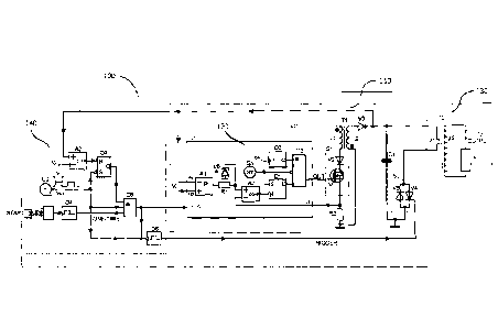
[0014] FIG. 1 depicts a functional circuit diagram of an ignition device 100
in accordance with
an example embodiment. The diagram depicts both functional block and discrete
elements.
[0015] FIG. 2 depicts timing diagrams for several signals in the ignition
device in accordance
with an example embodiment. As will be explained in more detail below, the
diagram shows,
among other things, that an unintentional unlimited start signal (START) is
internally limited to
a predefined limit (ONE-TIME signal). The next operation may be started after
removal of the
start signal and consequent start activation. The low frequency or pace
oscillator G2 in a
particular embodiment stops the operation. However in another embodiment, the
oscillator G2
may continue its operation, while the charging of the capacitor is disabled in
another way.
Trigger pulses (TRIGGER) fire the discharging switch are also shown. The last
time diagram
shows the voltage on the capacitor (Vci) during the cycle of the operation.
[0016] FIG. 3 depicts the time diagrams of the voltage on the charging
capacitor with an
increased time scale, to more clearly illustrate the charge and discharge
process and to show the
voltage levels \Tcii and Vco. The voltage level Vci2 is not shown in the
figure. Vc12 is expected
to be greater than Vcii, and lower than VC13, however these are not obligatory
conditions.
[0017] Referring to FIG. 1, in the ignition device 100, the charger 110, which
is configured as a
flyback converter, charges capacitor Cl. The charger 110 comprises coupled
inductor Ti with
primary winding of inductance Li and secondary winding of inductance L2, a
switch Si having
a reverse blocking capacity, presented as a serial connection of a MOSFET
transistor V1 and
CA 03063356 2019-11-12
WO 2018/215856 PCT/IB2018/053202
diode V2, secondary rectifier V3 and a pulse width modulation (PWM) control
circuit Ni 120
operating on the principle of the peak current mode (PCM).
[0018] PMW control circuit Ni 120 may be an integrated control circuit and
comprises oscillator
Gl, producing short pulses of high frequency fosc, voltage feedback amplifier
Al, and a
maximum current limiter in the form of resistor R1 and Zener diode V6. PMW
control circuit
Ni 120 further comprises peak current comparator A2, PWIVI latch D1, and
output logic element
(AND gate) D2. PMW control circuit Ni 120 may still further include a T-
trigger D3, which
divides the frequency of the operation (fosc) by, e.g., two and thus limits
the maximum duty
cycle to 50%. PMW control circuit Ni 120 includes a control input ON/ OFF ,
which starts and
stops the operation. Although not shown in the figure, the operation may be
stopped by, e.g.,
stopping oscillator GI, among other approaches, such that MOSFET V1 is
precluded from being
turned on, and such that current does not flow through the primary winding of
Ti.
[0019] The charger is supplied from an external direct current low voltage
supply VDC.
[0020] The ignition device 100 of the present embodiments further includes an
operation control
circuit 140 comprising low frequency oscillator G2, having a predefined
frequency and
generating pulses of predefined width ton (see FIGs. 2 and 3).
[0021] The signal from the low frequency oscillator G2 is applied to AND logic
gate D5
enabling the operation of the charger 110 only during the active pulse within
the ton time
through the control input ON/ OFF . Thus, the charger 110 operates during the
ton time. On the
down slope of the ton pulse, the trigger pulse is generated by the monoflop
D6. A switch S2 of
the reverse conductivity, presented as a thyristor V4 with a diode V5 is thus
activated closing the
CA 03063356 2019-11-12
WO 2018/215856 PCT/IB2018/053202
6
circuit of serial connection of the primary winding z1 of the high voltage
transformer T2, and the
capacitor Cl. Reverse conductivity through V5is required due to the resonant
character of the
discharge. The output winding z2 of the transformer T2 is connected to the gas
gap, i.e., the high
voltage output (HV OUTPUT) of high voltage output circuit 130. The high
voltage output
circuit 130 may include a clamping circuit F1. Once switch S2 (thyristor V4)
is activated, the
high voltage appears at the gas gap, ionizing the space between the
electrodes, thus creating the
conductive path to enable a low voltage GTWA arc. The GTWA welding power
supply
interconnection to the ignition device 100 is not depicted in FIG. 1 as it is
not relevant to the
present embodiments.
[0022] The charger 110 and PMW control circuit 120 work on the principle of a
flyback
converter in discontinuous current mode operation (DCM). Every pulse from the
oscillator GI
sets the PWM latch DI. On the downslope of the pulse from oscillator, the
control output OUT
activates the switch Si by applying an appropriate voltage to the gate of Vi.
Thus, the current in
the primary winding Li increases starting from the zero. The current is sensed
using resistor R2
and a current sense signal CS is delivered to the PWM control circuit
comparator A2. Once the
current reaches the value equal to the voltage on the + input of the
comparator A2 divided by the
resistance R2, the PWM control circuit latch D1 is reset, switching off the
output signal OUT.
The voltage on windings Ll , L2 reverses and the current in the coupled
inductor TI starts to flow
through the diode V5 charging the capacitor C I. The cycle is repeated on
every pulse of GI
oscillator.
[0023] Initially, the current in the winding Li increases to the certain
maximum value, defined
by the reference voltage Vz from the V6 reference diode, and the resistance of
R2. When the
CA 03063356 2019-11-12
WO 2018/215856 PCT/IB2018/053202
7
voltage of the capacitor Cl reaches the Vcii level (FIG. 2) the voltage
feedback amplifier Al
starts to decrease the current reference. Thus, the voltage feedback loop is
closed and the
charger keeps the voltage on the capacitor Cl at the level Wu. In this way the
voltage on the
capacitor is regulated in a first way.
[0024] Due to importance of the Vci voltage level, second, separate,
overvoltage protection is
implemented. Specifically, the comparator A3 resets the trigger D7 once
voltage Vc12 is
reached. The trigger D7 is reset on every absence of the pulse from pace
oscillator G2. Thus the
voltage on capacitor Cl cannot be greater than Vci2, even under a scenario in
which the voltage
feedback loop comprising voltage feedback amplifier Al does not work.
[0025] The maximum voltage on the capacitor Cl is limited in a third way to a
level VC13. Since
the peak current in the primary winding Ll of the coupled inductor T1 is
limited to the value
Vz/122, and the charging time is limited to the ton, the maximum voltage on
the capacitor Cl is
limited to the value:
Tiz iLi
VC13 = ¨R2 * * ton * fosc
[0026] If the PWM control circuit N1 120 includes T-trigger D3, then
i Li fasc
VC13 = ¨ * ¨ * ton * -
R2 C1 2
CA 03063356 2019-11-12
WO 2018/215856 PCT/IB2018/053202
8
[0027] Thus, in accordance with the embodiments described herein there is
provided an ignition
device that includes a charger, a pulse width modulation control circuit that
is configured to
control charging of a capacitor of the charger, a high voltage output circuit
electrically connected
to the capacitor and comprising a switch that enables the capacitor to be
discharged, and an
operation control circuit that controls the switch to cause a high voltage to
be present at an output
of the high voltage output circuit
[0028] The embodiments described herein provide several distinctive features,
including a
charger employing a flyback converter with a switch having a reverse blocking
capacity, triple
control over the charging voltage, and a limited ignition operation time.
[0029] More specifically, the accumulating capacitor Cl is charged from the
flyback converter
with switch Si having a reverse blocking capacity as a result of diode V2.
Diode V2 protects the
converter and the voltage supply VDC against reverse voltage, which appears
during the
resonance of the accumulating capacitor Cl and the external inductances and
capacitances.
[0030] The maximum voltage on the accumulating capacitor Cl is limited in
three ways. First,
the flyback converter has accurately defined momentary power and accurately
defined time of
the operation. The capacitor has accurate capacitance. In this way, the
portion of energy and
consequently the maximum capacitor's voltage is well defined. Second, the
flyback converter
comprises a voltage feedback loop via Al, thus the capacitor's voltage is well
defined. Third, a
backup voltage feedback loop via A3 with latch D7 disables the operation of
the flyback
converter when the capacitor's voltage is too high.
[0031] Finally, the one-time operation of the unit is internally limited. On
presence of the
START signal on the input of the timer D4, its output (ONE-TIME signal) is
activated, but only
CA 03063356 2019-11-12
WO 2018/215856 PCT/IB2018/053202
9
for time not longer than a predefined or predetermined time. Further, the
output of the timer D4
is not active in absence of the START signal. The ONE-TIME signal enables the
operation of
the unit by means of the gate D5. In this way the equipment is protected
against a general failure
wherein the unit is driven by an inadvertently applied permanent START signal.
In addition, due
to this time limit, total energy and total charge delivered by the unit within
one cycle of welding
are limited.
[0032] The above description is intended by way of example only. Various
modifications and
structural changes may be made therein without departing from the scope of the
concepts
described herein and within the scope and range of equivalents of the claims.