Note: Descriptions are shown in the official language in which they were submitted.
CA 03063861 2019-11-15
WO 2018/222251 PCT/US2018/023721
1
ADDRESS ASSIGNMENT SYSTEM AND METHOD FOR SURGICAL
LIGHTHEAD COMPONENTS
Field of the Invention
[0001] The present invention relates generally to a system and method for
address
assignment, and more particularly, to a system and method for assigning
addresses to
components of a surgical lighthead that share a common communication bus.
Background of the Invention
[0002] A typical computer system is comprised of a control system (e.g.,
microprocessor or microcontroller) and one or more components. The components
are
connected with the control system to allow the transfer of information (e.g.,
instructions
and/or data) therebetween. In the implementation of some computer systems,
each
component is directly wired to the control system. Accordingly, a separate
wired connection
is provided for each component. This allows the control system to
independently
communicate with each component. However, separate wiring of each component to
the
control system can be complex, time consuming, and error prone.
[0003] In order to simplify the wiring, the control system and all the
associated
components are connected to a common bus (also referred to as a "shared bus").
When a
common bus is used, each component must have an assigned address, so that each
component can recognize which instructions from the control system are
intended for that
component. In other words, since all of the information communicated between
the control
system and the components travels through the common bus, each of the
components must
be able to distinguish which information is intended for that component.
[0004] In the implementation of some computer systems, jumpers and dip
switches
on each component are used to establish an address in a hardware setting for
that component.
For example, the jumpers or dip switches on a first component may be set to
address 0001 to
establish a first address, while the jumpers or dip switches on a second
component may be set
to address 0010, to establish a second address. However, if there are many
components in
the computer system, it can be time consuming to set jumpers or dip switch
settings for each
CA 03063861 2019-11-15
WO 2018/222251 PCT/US2018/023721
2
component. Also, an error in setting the jumpers or dip switches will result
in
malfunctioning of the computer system.
[0005] Surgical lighting systems used in a surgical suite are typically
comprised of a
computer system that includes a main computer control unit and one or more
lightheads,
wherein each lighthead has a plurality of light modules. Each light module may
include a
control unit, one or more LED strings, and one or more sensors (e.g., light
sensors, distance
sensors, and the like). In order to simplify the manufacturing process, the
main computer
control unit and the plurality of light modules may be connected to a common
bus, as
described above. For proper communication between the main computer control
system and
the light modules, each light module must have an assigned address for
identifying a specific
light module on the common bus. As indicated above, there are some significant
drawbacks
to using jumpers and/or dip switches to assign an assigned address to each
component in
hardware.
[0006] The present invention provides an address assignment system and
method that
overcomes these and other drawbacks of the prior art.
Summary of the Invention
[0007] In accordance with the present invention, there is provided a
method for
assigning addresses to a plurality of components sharing a common bus, wherein
each
component has at least two operating states, said method comprising: (a)
establishing all
components needing an address assignment as active components; (b) selecting a
target
component among the plurality of components that is to be assigned an address
for
communication therewith; (c) setting all active components to a random state
by transmitting
an instruction to the plurality of components to select a random state; (d)
detecting the
current state of the target component, wherein the current state is
established as state X; (e)
deactivating all of the components that do not match state X, wherein
deactivated
components are removed from evaluation for address assignment; and (f)
determining if the
target component is the only remaining active component among the plurality of
components, wherein (i) if the target component is the only remaining active
component,
then assigning an address to the target component, deactivating the target
component, and
CA 03063861 2019-11-15
WO 2018/222251 PCT/US2018/023721
3
repeating steps (a)-(f) for components still needing an address assignment,
and (ii) if the
target component is not the only remaining active component, then repeating
steps (c)-(f).
[0008] In accordance with another aspect of the present invention, there
is provided a
method for assigning addresses to a plurality of components connected to a
common bus,
each component having a respective distance sensor, said method comprising:
locating the
sensors of the plurality of components relative to a calibration plank having
a sloped front
face, wherein each sensor is a different distance from the sloped front face;
instructing the
plurality of components to have the respective sensors take a distance reading
indicative of
the distance to the front face of the calibration plank; instructing the
plurality of components
to self-assign an address based upon the distance reading indicative of the
distance to the
front face of the calibration plank.
[0009] In accordance with still another aspect of the present invention,
there is
provided a system for assigning addresses to a plurality of light modules
sharing a common
bus, said system comprising: a calibration unit having a control system and a
sensing device
for detecting at least one lighting parameter of the plurality of light
modules, the calibration
unit programmed to: (a) establish all light modules needing an address
assignment as active
light modules; (b) select a target light module among the plurality of light
modules that is to
be assigned an address for communication therewith; (c) set all active light
modules to a
random state by transmitting an instruction to the plurality of light modules
to select a
random state, wherein each state includes one or more lighting parameters; (d)
detect the
current state of the target light module, wherein the current state is
established as state X; (e)
deactivate all of the light modules that do not match state X, wherein
deactivated light
modules are removed from evaluation for address assignment; and (f) determine
if the target
light module is the only remaining active light module among the plurality of
light modules,
wherein (i) if the target light module is the only remaining active light
module, then
assigning an address to the target light module, deactivating the target light
module, and
repeating steps (a)-(f) for light modules still needing an address assignment,
and (ii) if the
target light module is not the only remaining active light module, then
repeating steps (c)-(f).
[0010] An advantage of the present invention is the provision of an
address
assignment system and method that is fast and accurate.
CA 03063861 2019-11-15
WO 2018/222251 PCT/US2018/023721
4
[0011] Another advantage of the present invention is the provision of an
address
assignment system and method that can be automated.
[0012] A still further advantage of the present invention is the
provision of an address
assignment system and method that facilitates the manufacture and servicing of
devices
having components that are connected to a common communication bus.
[0013] Yet another advantage of the present invention is the provision of
an address
assignment system and method that does not add complexity to existing devices
in order to
assign addresses.
[0014] These and other advantages will become apparent from the following
description of illustrated embodiments taken together with the accompanying
drawings and
the appended claims.
Brief Description of the Drawings
[0015] The invention may take physical form in certain parts and
arrangement of
parts, embodiments of which will be described in detail in the specification
and illustrated in
the accompanying drawings which form a part hereof, and wherein:
[0016] FIG. 1 is a block diagram of an address assignment system
according to an
embodiment of the present invention, for assigning addresses to a plurality of
devices
connected to a common bus;
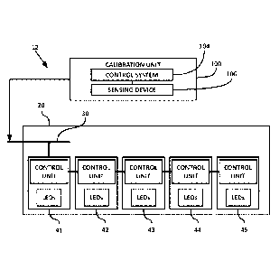
[0017] FIG. 2 is a block diagram of an address assignment system,
according to an
embodiment of the present invention, for assigning addresses to a plurality of
light modules
of a surgical lighthead that are connected to a common bus;
[0018] FIG. 3 is a flow chart of an address assignment method according
to an
embodiment of the present invention, the method using an iterative elimination
process for
assigning addresses to the plurality of light modules connected to the common
bus, as shown
in FIG. 2;
[0019] FIG. 4 is a sequence diagram of the address assignment method
shown in FIG.
3;
[0020] FIGS. 5-10 show the state of light modules of a lighthead during a
process of
assigning an address to one of the light modules using the iterative
elimination process;
CA 03063861 2019-11-15
WO 2018/222251 PCT/US2018/023721
[0021] FIG. 11 is a block diagram of an address assignment system for
assigning
addresses to a plurality of light modules, according to an alternative
embodiment of the
present invention; and
[0022] FIG. 12 is a flow chart of an address assignment method according
to the
alternative embodiment of the present invention.
Detailed Description of the Invention
[0023] Referring now to the drawings wherein the showings are for the
purposes of
illustrating an embodiment of the invention only and not for the purposes of
limiting same,
FIG. 1 shows a block diagram of an address assignment system 10 for assigning
addresses to
a plurality of devices D1-D5 that are connected to a common bus 8. This
illustrated
embodiment is a general application of the address assignment system of the
present
invention. Address assignment system 10 includes a calibration unit 60 having
a control
system 64. Control system 64 includes a microprocessor or microcontroller and
memory
storage. Calibration unit 60 is connected to common bus 8 to communicate with
a plurality
of devices D1-D5. Instructions and/or data transmitted via common bus 8 are
used to assign
addresses to each device D1-D5, as will explained in detail with reference to
the
embodiments discussed below. The assignment of addresses allows each device D1-
D5 to be
identified in an instruction intended for that device, and allows each device
to identify data
transmitted by that device. In this way, information can be transmitted to a
specific device,
and each device can identify the information transmitted by that device.
[0024] Referring now to FIG. 2, there is shown a block diagram of an
address
assignment system 12 for assigning addresses to a plurality of light modules
41-45 of a
surgical lighthead 20 that are connected to a common bus 30. Address
assignment system 12
is comprised of a calibration unit 100 that includes a control system 104 and
a sensing device
106 connected thereto. Control system 104 is substantially the same as control
system 64
described above. Sensing device 106 is used to detect the state of light
modules, as will be
described below. In the illustrated embodiment, sensing device 106 takes the
form of a
machine vision camera having one or more image sensors (e.g., CCD or CMOS
image
sensor).
CA 03063861 2019-11-15
WO 2018/222251 PCT/US2018/023721
6
[0025] Lighthead 20 includes a plurality of light modules 41-45. Each
light module
41-45 includes a control unit and a plurality of LEDs (e.g., an LED string)
connected thereto.
Each control unit has a microcomputer or microcontroller, and memory storage.
Light
modules 41-45 may also include other components, including, but not limited
to, an LED
driver, a power regulation circuit, and one or more sensors (e.g., light
and/or distance
sensors). Each control unit controls lighting parameters of respective LEDs
(e.g., light
intensity, color, color temperature, and the like).
[0026] In an illustrated embodiment, light modules 41-45 are connected to
common
bus 30. More specifically, the control units of light modules 41-45 are
connected to common
bus 30 in a daisy chain wiring scheme. It is contemplated that light modules
41-45 may be
connected to common bus 30 using alternative wiring configurations.
Furthermore, it should
be appreciated that the number of light modules shown in FIG. 2 is solely for
the purpose of
illustrating an embodiment of the present invention. Thus, it is contemplated
that lighthead
20 may have a larger or smaller number of light modules.
[0027] An address assignment method 150 that uses an iterative
elimination process
to assign addresses to the light modules will now be described with reference
to FIGS. 3-4
and 5-10. FIG. 3 provides a flow chart of method 150 and FIG. 4 provides a
sequence
diagram of method 150. For greater clarity, the step numbers shown in FIG. 3
are also
referenced in FIG. 4. FIGS. 5-10 illustrate the state of each light module of
a lighthead using
method 150 to assign an address to light module 45.
[0028] For the purpose of describing address assignment method 150, it is
assumed
solely for the sake of simplicity that light modules 41-45 have only two (2)
operating states
(i.e., OFF and ON). However, as will be discussed in detail below, it should
be appreciated
that light modules 41-45 may have more than two (2) operating states.
[0029] Assignment of an address to a selected target light module (i.e.,
light module
45) will now be described. As an initialization step (step 152), control
system 104 of
calibration unit 100 transmits an instruction to lighthead 20 commanding all
light modules
41-45 to the OFF state (FIG. 5), followed by transmission of an instruction to
lighthead 20
commanding all of the light modules 41-45 to the ON state (FIG. 6).
Instructions sent to
lighthead 20 via common bus 30 are received by the control unit of each light
module 41-45,
which in turn, controls the LEDs (i.e., turns the LEDs OFF and then ON).
Sensing device
CA 03063861 2019-11-15
WO 2018/222251 PCT/US2018/023721
7
106 of calibration unit 100 is used to verify that all light modules 41-45 are
in the
commanded OFF or ON state, thereby confirming that all of the light modules 41-
45 are
operating properly.
[0030] Next, all of the light modules that need address assignments are
made active
(step 153). Light modules are active if they are considered for address
assignment by control
system 104 of calibration unit 100. In step 154, control system 104 transmits
an instruction
to lighthead 20 commanding each active light module 41-45 to select a random
operating
state (i.e., ON state or OFF state). Accordingly, the control units of each
light module 41-45
receives the instruction from control system 104, and commands all of LEDs
associated
therewith to either an ON state or an OFF state (FIG. 7). In FIG. 7, light
modules 41 and 43
have been randomly set to the OFF state (i.e., all associated LEDs are turned
OFF), while
light modules 42, 44, and 45 have been randomly set to the ON state (i.e., all
associated
LEDs are turned ON).
[0031] Sensing device 106 detects the current operating state (State X)
of light
module 45 (step 156). In the illustrated example shown in FIG. 7, State X is
in the ON state.
All active light modules 41-45 that do not match State X (i.e., the ON state)
are deactivated
and thereby removed from consideration in address assignment process 150 (step
158).
Deactivated light modules are shown in the figures with an "X." When a light
module is
deactivated, control system 104 no longer considers the state of the
associated LEDs as
detected by sensing device 106. Accordingly, light modules that are
deactivated are removed
from consideration in the address assignment method.
[0032] Next, it is determined whether the target light module (i.e.,
light module 45) is
the only remaining active light module of lighthead 20 (step 160). In the
illustrated example,
there remain three (3) active light modules, i.e., light modules 42, 44, and
45. Therefore,
address assignment method 150 returns to step 154, and all active light
modules are again set
to a random state. As shown in FIG. 8, the target light module (i.e., light
module 45) and
light module 42 have been randomly set to the OFF state, while light module 44
has been
randomly set to the ON state. The current state (State X) of light module 45
is detected (step
156), and State X is determined to be the OFF state. Accordingly, light module
44, which
does not match State X, is deactivated (step 158). At step 160 it is
determined whether the
target light module (i.e., light module 45) remains the only active light
module. Since two
CA 03063861 2019-11-15
WO 2018/222251 PCT/US2018/023721
8
light modules (i.e., light modules 42 and 45) remain active, address
assignment method 150
returns once again to step 154.
[0033] The light modules 42 and 45 are again set to a random state. As
shown in
FIG. 9, the target light module (i.e., light module 45) has been randomly set
to the OFF state,
while light module 42 has been randomly set to the ON state. The current state
(State X) of
light module 45 is detected (step 156), and State X is determined to be the
OFF state.
Accordingly, light module 42, which does not match State X, is deactivated
(step 158), as
shown in FIG. 10.
[0034] At step 160, it is determined that the target light module (i.e.,
light module 45)
is the only active light module of lighthead 20. Accordingly, address
assignment method 150
proceeds to step 162, where address Y is assigned to light module 45. In this
regard, address
Y is stored in non-volatile memory of the control unit of light module 45.
Next, the address
assignment of light module 45 is verified by first setting all of the light
modules 41-45 to the
OFF state, and then setting only light module 45 to the ON state by sending an
instruction
with address Y. If sensing device 106 only detects light module 45 as being in
the ON state,
then the address assignment has been successful. At step 166, light module 45
is deactivated
for the purpose of any further address assignments. Accordingly, as each
target light module
is assigned an address, it is deactivated to remove it from any subsequent
processing steps for
assigning addresses to the other light modules.
[0035] If it is determined at step 168 that all of the light modules 41-
45 have been
assigned addresses, then address assignment method 150 ends. Otherwise,
address
assignment method 150 returns to step 153 to assign an address to another
target light
module. Accordingly, steps 153-168 of address assignment method 150 are
repeated to
assign addresses to the remaining light modules 41-44.
[0036] As mentioned above, light modules 41-45 may have more than two (2)
operating states. These additional operating states may involve various
lighting parameters
of the light modules, including, but not limited to, light intensity level,
color, color
temperature, blinking rate, and pulsing frequency. Therefore, it is
contemplated that address
assignment method 150 may be implemented using a combination of the operating
states
relating to various lighting parameters. For example, the operating states
used in the address
assignment method 150 could include the following nine (9) operating states:
CA 03063861 2019-11-15
WO 2018/222251 PCT/US2018/023721
9
STATE 1: OFF
STATE 2: ON / light intensity level 1 / warm color
STATE 3: ON / light intensity level 1 / cool color
STATE 4: ON / light intensity level 2 / warm color
STATE 5: ON / light intensity level 2 / cool color
STATE 6: ON / light intensity level 3 / warm color
STATE 7: ON / light intensity level 3 / cool color
STATE 8: ON / light intensity level 4 / warm color
STATE 9: ON / light intensity level 4 / cool color
[0037] In the foregoing example, the random state for each light module
is selected
from one of nine (9) unique operating states. As will be appreciated, with a
sufficiently large
number of unique operating states, the number of iterations needed to assign
addresses to
each light module can be significantly reduced, thereby speeding the address
assignment
process.
[0038] Referring now to FIG. 11, an alternative embodiment of the present
invention
will be described. Address assignment system 14 is comprised of a calibration
unit 100
having a control system 104, and a calibration plank 110 having a sloping
front face 112.
[0039] As indicated above, each light module of a lighthead 20 may also
include one
or more sensors (e.g., light and/or distance sensors). In the embodiment shown
in FIG. 11,
each light module 41-45 of lighthead 20 includes a respective distance sensor
81-85. Each
distance sensor 81-85 is connected to the respective control unit of the light
module. As can
be seen in FIG. 11, a unique distance is provided between front face 112 of
calibration plank
110 and each sensor 81-85. The distances detected between sensors 81-85 and
front face 112
of calibration plank 100 are used to assign an address to each light module 41-
45.
[0040] In accordance with this embodiment of the present invention,
control system
104 of calibration unit 100 stores an assigned address in the non-volatile
memory of the
control units of light modules 41-45 based upon the distance sensed by the
associated
distance sensor 81-85. Accordingly, unique readings from distance sensors 81-
85 are used to
assign addresses to light modules 41-45.
CA 03063861 2019-11-15
WO 2018/222251 PCT/US2018/023721
[0041] Referring now to FIG. 12, there is shown a flow chart illustrating
the steps of
address assignment method 180 according to the alternative embodiment of the
present
invention. Control system 104 transmits instructions via common bus 30 that
are received by
the control units of light modules 41-45. A first instruction is broadcast to
the control units
of light modules 41-45 commanding the control units to have respective sensors
81-85 take a
distance reading (step 182). At step 184, control system 104 broadcasts an
instruction to the
control units that commands the control units to self-assign an address based
upon the value
of the distance reading detected by the sensors 81-85. For example, the
instruction may
command the control units to self-assign an address, as follows:
= If sensor detects a distance of 2.5m +/- 0.1m to front face 112, then
self-assign address 1 by storing address 0000 in the non-volatile
memory of the control unit (steps 186, 196).
= If sensor detects a distance of 2.0m +/- 0.1m to front face 112, then
self-assign address 2 by storing address 0001 in the non-volatile
memory of the control unit (steps 188, 198).
= If sensor detects a distance of 1.5m +/- 0.1m to front face 112, then
self-assign address 3 by storing address 0010 in the non-volatile
memory of the control unit (steps 190, 200).
= If sensor detects a distance of 1.0m +/- 0.1m to front face 112, then
self-assign address 4 by storing address 0011 in the non-volatile
memory of the control unit (steps 192, 202).
= If sensor detects a distance of 0.5m +/- 0.1m to front face 112, then
self-assign address 5 by storing address 0100 in the non-volatile
memory of the control unit (steps 194, 204).
[0042] The distances from the sensor to front face 112 of calibration
plank 110 are
pre-stored in the memory of control system 104. These pre-stored distances are
inserted into
the instruction broadcast to the control units for self-assigning addresses to
light modules 41-
45.
CA 03063861 2019-11-15
WO 2018/222251 PCT/US2018/023721
11
[0043] It should be appreciated that the distance values provided above
are solely for
the purpose of illustrating an embodiment of the present invention, and are
not intended to
limit same. Moreover, the number of light modules in lighthead 20 may vary
from those
shown in the illustrated embodiment shown in FIG. 11. Furthermore, the same
address can
be self-assigned to multiple light modules by physically modifying front face
112 of
calibration plank 110, and thereby provide the same distance to multiple
sensors. By
assigning the same address to more than one light module, a group of two or
more light
modules will respond to an instruction identifying that address.
[0044] In the embodiments of the present invention illustrated in FIGS. 2
and 11 light
modules 41-45 are shown as being directly connected to common bus 30. It
should be
appreciated that lighthead 20 may also include a supervisory controller that
is connected
between light modules 41-45 and common bus 30. Accordingly, light modules 41-
45 are not
directly connected to common bus 30, and calibration unit 100 communicates
with light
modules 41-45 via the supervisory controller.
[0045] The foregoing describes specific embodiments of the present
invention. It
should be appreciated that these embodiments are described for purposes of
illustration only,
and that numerous alterations and modifications may be practiced by those
skilled in the art
without departing from the spirit and scope of the invention. For example, it
is contemplated
that the address assignment system and method of the present invention may be
used to
assign addresses to components other than those of a surgical lighthead. The
present
invention finds utility in any system where a common bus is shared for
communications with
a plurality of components. It is intended that all such modifications and
alterations be
included insofar as they come within the scope of the invention as claimed or
the equivalents
thereof.