Note: Descriptions are shown in the official language in which they were submitted.
CA 03063958 2019-11-15
WO 2018/213799 PCT/US2018/033532
INVERTER-BASED DIFFERENTIAL AMPLIFIER
TECHNICAL FIELD
[0001] This disclosure relates to electrical amplifier circuits and, more
particularly, to an
inverter amplifier comparator.
BACKGROUND
[0002] Certain previous architectures are configured for low noise, high
speed differential
amplifiers that act as a simple differential pair with load resistors and a
differential inverter
amplifier topology. For low noise high speed applications, simplicity may be
useful because
additional complexity may degrade noise performance, bandwidth, or both. For
portable,
battery operated devices, efficiently employing current may be useful.
[0003] FIGURE 1 illustrates an example of a previous topology 100
incorporating a
metal oxide semiconductor (MOS) differential pair for gain and resistive
loads. This circuit
provides low noise, reasonable gain, and high bandwidth. FIGURE 2 illustrates
alternating
current (AC), noise, and transient performance 200 of the topology 100
illustrated by
FIGURE 1 for the device size and technology shown.
[0004] Whereas a differential pair with load resistors is a low noise
topology, amplifier
topologies using both negative channel MOS (NMOS) and positive channel MOS
(PMOS)
differential pair configurations may be employed. These inverter amplifier
topologies may
provide improvement in performance because the bias current is used to
generate gain (gm)
in both the NMOS and PMOS pairs. FIGURE 3 illustrates an example of a previous
differential inverter amplifier topology 300 in which the bias current flows
through both the
PMOS and NMOS differential pairs, effectively doubling the available gm for
properly
optimized device sizing. A replica bias circuit is used to set the NMOS and
PMOS bias
-1-
CA 03063958 2019-11-15
WO 2018/213799 PCT/US2018/033532
current. Here, vcm is externally set to vdd/2 and the replica bias circuit
adjusts so that the
gates of the PMOS & NMOS current sources are also at vdd.
[0005] The differential inverter amplifier 300 illustrated by FIGURE 3 may
be employed
for a high signal limiting stage such as the clock buffer in the reference.
However, there are
severe problems that make such a system inadequate for a high speed low noise
amplifier
stage for an input signal with a large dynamic range. The comparator for a
Successive
Approximation Register (SAR) Analog to Digitial Converter (ADC) is one such
application.
[0006] FIGURE 4 shows results 400 demonstrating that the output common mode
voltage is about 850mV compared to a desired output common mode of vcm =
vdd/2. Since
the gates of both the NMOS and PMOS current sources are tied together at a
node labeled
vgn in FIGURE 4, the voltage is near half of vdd. This makes the circuit
sensitive to device
parameters and difficult to balance at the desired output common mode voltage.
FIGURE 6
shows the results 600 of a Monte Carlo mismatch simulation and that the output
common
mode varies over a large portion of the supply range, which may cause the
circuit to exhibit
excessive variation of gain and bandwidth. Furthermore, the circuit may become
inoperable
at extremes of common mode voltage due to headroom issues.
[0007] In addition to the issue of excessive common mode variation, the
circuit 300
illustrated by FIGURE 3 may exhibit limiting behavior that is signal
dependent, which is
undesirable in a SAR application because such behavior may cause distortion. A
comparison
between FIGURES 4 and 5 shows that the output common mode voltage and the two
common source nodes labeled vsp and vsn exhibit strikingly different behavior
between the
30mV and 500mV input signal cases.
[0008] This circuit 300 has three different modes of operation depending on
the input
signal: a small signal with no limiting and the input devices operating in the
active region; a
medium signal with the input switch devices entering the triode region and
acting as
- 2 -
CA 03063958 2019-11-15
WO 2018/213799 PCT/US2018/033532
switches; and a large signal with the input devices acting as switches and the
current sources
entering the triode region due to low headroom. The small and medium signal
modes may
not be problematic, but the large signal mode where the current sources are
being crushed
should be avoided.
[0009] Embodiments of the disclosed technology address these and other
limitations in
the prior art.
BRIEF DESCRIPTION OF THE DRAWINGS
[0010] FIGURE 1 illustrates an example of a previous topology incorporating
a metal
oxide semiconductor (MOS) differential pair for gain and resistive loads.
[0011] FIGURE 2 illustrates alternating current (AC), noise, and transient
performance of
the topology illustrated by FIGURE 1.
[0012] FIGURE 3 illustrates an example of a previous differential inverter
amplifier
topology.
[0013] FIGURE 4 illustrates an example of a small signal response of an
inverter
amplifier with replica bias.
[0014] FIGURE 5 illustrates an example of a large signal response of an
inverter
amplifier with replica bias.
[0015] FIGURE 6 illustrates an example of a Monte Carlo variation of an
inverter
amplifier with replica bias.
[0016] FIGURE 7 illustrates an example of a differential inverter amplifier
with
separated common mode feedback of replica bias in accordance with certain
embodiments of
the disclosed technology.
[0017] FIGURE 8 illustrates an example of a small signal response of the
inverter
amplifier with separated common mode feedback of replica bias illustrated by
FIGURE 7.
- 3 -
CA 03063958 2019-11-15
WO 2018/213799 PCT/US2018/033532
[0018] FIGURE 9 illustrates an example of a large signal response of the
inverter
amplifier with separated common mode feedback of replica bias illustrated by
FIGURE 7.
[0019] FIGURE 10 illustrates an example of a Monte Carlo variation of the
inverter
amplifier with separated common mode feedback of replica bias illustrated by
FIGURE 7.
[0020] FIGURE 11 illustrates an example of a differential inverter
amplifier with output
common mode feedback in accordance with certain embodiments of the disclosed
technology.
[0021] FIGURE 12 illustrates an example of a small signal response of the
inverter
amplifier with output common mode feedback illustrated by FIGURE 11.
[0022] FIGURE 13 illustrates an example of a large signal response of the
inverter
amplifier with output common mode feedback illustrated by FIGURE 11.
[0023] FIGURE 14 illustrates an example of a Monte Carlo variation of the
inverter
amplifier with output common mode feedback illustrated by FIGURE 11.
[0024] FIGURE 15 illustrates an example of a differential inverter
amplifier with output
common mode feedback and load resistors in accordance with certain embodiments
of the
disclosed technology.
[0025] FIGURE 16 illustrates an example of a small signal response of the
inverter
amplifier with output common mode feedback and load resistors illustrated by
FIGURE 15.
[0026] FIGURE 17 illustrates an example of a large signal response of the
inverter
amplifier with output common mode feedback and load resistors illustrated by
FIGURE 15.
[0027] FIGURE 18 illustrates an example of a differential inverter
amplifier with load
resistors connected to vcm=vdd/2 in accordance with certain embodiments of the
disclosed
technology.
[0028] FIGURE 19 illustrates an example of a small signal response of the
inverter
amplifier with load resistors connected to vcm=vdd/2 illustrated by FIGURE 18.
- 4 -
CA 03063958 2019-11-15
WO 2018/213799 PCT/US2018/033532
[0029] FIGURE 20 illustrates an example of a large signal response of the
inverter
amplifier with load resistors connected to vcm=vdd/2 illustrated by FIGURE 18.
[0030] FIGURE 21 illustrates an example of a Monte Carlo variation of the
inverter
amplifier with output common mode feedback illustrated by FIGURE 18.
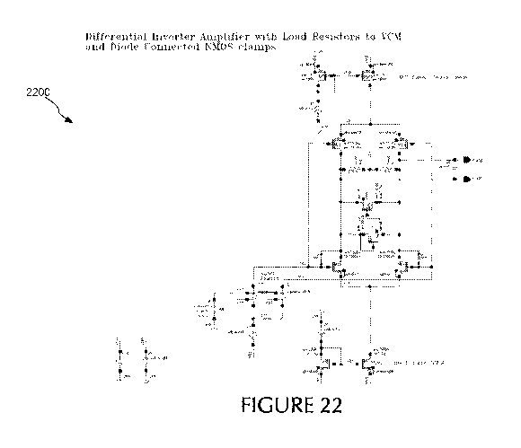
[0031] FIGURE 22 illustrates an example of a differential inverter
amplifier with load
resistors connected to vcm=vdd/2 and diode connected clamp devices in
accordance with
certain embodiments of the disclosed technology.
[0032] FIGURE 23 illustrates an example of a small signal response of the
inverter
amplifier with load resistors connected to vcm=vdd/2 and diode connected clamp
devices
illustrated by FIGURE 22.
[0033] FIGURE 24 illustrates an example of a small signal response of the
inverter
amplifier with load resistors connected to vcm=vdd/2 and diode connected clamp
devices
illustrated by FIGURE 22.
[0034] FIGURE 25 illustrates an example of a Monte Carlo variation of the
inverter
amplifier with load resistors connected to vcm=vdd/2 and diode connected clamp
devices
illustrated by FIGURE 22.
DETAILED DESCRIPTION
[0035] Certain implementations of the disclosed technology address the
common mode
issues described above and provide output limiting to prevent the current
sources from
entering the triode region. In certain embodiments, a separate bias current
setting and
common mode voltage control may be employed. Diode-connected metal oxide
semiconductor (MOS) clamps may be used to limit output swing and minimize
common
mode disturbances. A differential resistive load may be used to improve
bandwidth and
minimize common mode disturbances. A connection of load resistors may be used
to cause a
- 5 -
CA 03063958 2019-11-15
WO 2018/213799 PCT/US2018/033532
common mode voltage (vcm) equal to half of the voltage drain (vdd) in order to
omit an
output common mode control. A combination of load resistors and diode-
connected lamps
may be used to allow independent optimization of gain/bandwidth.
[0036] FIGURE 7 illustrates an example of a differential inverter amplifier
700 with
separated common mode feedback of replica bias in accordance with certain
embodiments of
the disclosed technology. In the example topology 700, the replica bias
circuit has been
separated into two parts: the first part is a PMOS mirror and current source
connected to the
PMOS differential pair, and the second part is a NMOS current source
controlled by a
feedback amplifier. The NMOS and PMOS current source nodes vgn and vgp may be
separated so that one current source (here, the PMOS) provides the bias
current, and the other
current source (here, the NMOS) is adjusted by a feedback loop to set the
common mode
voltage.
[0037] In this example 700, the common mode voltage vcm is externally
connected to
vdd/2 and the circuit 700 is configured to adjust the center of the replica
bias to also be at
vdd/2. The arrangement of the devices in the replica bias are intended to
mimic the devices
in the amplifier.
[0038] FIGURES 8, 9, and 10 illustrate example performance plots 800, 900,
and 1000,
respectively, that demonstrate that the output common mode may be balanced at
vdd/2, but
the circuit 700 still exhibits signal dependent limiting behavior and
excessive Monte Carlo
variation of output common mode. For a production circuit, the yield
implication of such
large variations may be problematic. The example shows that the two current
sources are
separated into one fixed current source and a second controlled source to set
the common
mode voltage.
[0039] The plot 800 illustrated by FIGURE 8 demonstrates that the circuit
provides high
gain, low bandwidth, and output common mode of 600mV. The plot 900 illustrated
by
- 6 -
CA 03063958 2019-11-15
WO 2018/213799 PCT/US2018/033532
FIGURE 9 demonstrates that the circuit exhibits high gain, low bandwidth, and
output
common mode variation. The plot 1000 illustrated by FIGURE 10 demonstrates
that the
circuit may exhibit excessive output common mode variation.
[0040] FIGURE 11 illustrates an example of a differential inverter
amplifier 1100 with
output common mode feedback in accordance with certain embodiments of the
disclosed
technology. The topology 1100 illustrated by FIGURE 11 includes a PMOS current
source
and an NMOS current source and output common mode feedback. In the example,
the
topology 1100 extends the concepts of the topology 700 illustrated by FIGURE 7
by sensing
the common mode at the actual output of the amplifier instead of at a replica
bias circuit.
[0041] In this example 1100, the common mode voltage vcm is again connected
to vdd/2
externally. But with this circuit 1100, the output common mode of the
amplifier is
configured to be directly sensed by the two large resistors such that the
output common mode
is adjusted to vdd/2 directly.
[0042] FIGURES 12, 13, and 14 illustrate performance plots 1200, 1300, and
1400,
respectively, that demonstrate that the output common mode is centered at
vcm=vdd/2 and
now has reasonable Monte Carlo variation. However, FIGURE 13 demonstrates that
the
current source nodes vsp and vsn are reaching supply and ground for large
input signals.
Stability of the common mode loop may also be a concern since the feedback
becomes
broken when the current sources run out of headroom.
[0043] The plot 1200 illustrated by FIGURE 12 demonstrates that that the
circuit exhibits
high gain, low bandwidth, and output common mode of 600mV. The plot 1300
illustrated by
FIGURE 13 demonstrates that the circuit exhibits high gain, low bandwidth, and
output
common mode variation. The plot 1400 illustrated by FIGURE 14 demonstrates
that the
circuit exhibits reasonable output common mode variation.
- 7 -
CA 03063958 2019-11-15
WO 2018/213799 PCT/US2018/033532
[0044] FIGURE 15 illustrates an example of a differential inverter
amplifier 1500 with
output common mode feedback and load resistors in accordance with certain
embodiments of
the disclosed technology. In the example, the load resistors in the amplifier
1500 have been
reduced from the high value common mode sensing resistors (e.g., the resistors
in the circuit
1100 illustrated by FIGURE 11) to a smaller value (e.g., 3 kiloohms (kohms)).
This may
limit the differential output voltage to the value of the bias current times
twice the load
resistor (e.g., (Vout max=Ibias*2*Rload)). The maximum differential output
swing may be
set to a value sufficiently below the available supply voltage to provide
headroom for both
the NMOS and PMOS current sources.
[0045] Similar to the topology 1100 of FIGURE 11, the common mode voltage
vcm in
this topology 1500 is connected to vdd/2 externally but the output common mode
of the
amplifier is configured to be directly sensed by the two large resistors such
that the output
common mode is adjusted to vdd/2 directly.
[0046] The performance plots 1600 and 1700 illustrated by FIGURES 16 and
17,
respectively, show that the maximum output swing has been reduced, the
bandwidth has been
increased due to reduced gain, and the output common mode is now well
controlled. The plot
1600 illustrated by FIGURE 16 demonstrates that the circuit exhibits reduced
gain, high
bandwidth, and output common mode of 600mV. The plot 1700 illustrated by
FIGURE 17
demonstrates that the circuit provides reduced gain, high bandwidth, and
output common
mode of 600mV.
[0047] The circuit 1500 illustrated by FIGURE 15 solves the common mode and
limiting
issues, but it still employs a common mode feedback circuit. The plots 1600
and 1700 of
FIGURES 16 and 17, respectively, indicate that there may be some concerns that
common
mode response may disrupt the differential signal. There are methods to ensure
sufficient
- 8 -
CA 03063958 2019-11-15
WO 2018/213799 PCT/US2018/033532
common mode stability and minimize common mode perturbations. However,
avoidance of
a common mode feedback loop could be useful.
[0048] Successive Approximation Register (SAR) Analog-to-Digital Converters
(ADCs)
may have an externally filtered common mode voltage (vcm) available. FIGURE
18, which
illustrates an example of a differential inverter amplifier 1800 with load
resistors connected
to vcm=vdd/2 in accordance with certain embodiments of the disclosed
technology, has been
modified to connect the 3000 (3k) load resistors directly to vcm. This allows
for the
omission of a common mode feedback loop.
[0049] The performance plots 1900 and 2000 illustrated by FIGURES 19 and
20,
respectively, demonstrate that the perturbations of the output common mode
voltage and the
common source nodes labeled vsp and vsn have been reduced considerably, e.g.,
compared to
the plots 1600 and 1700 illustrated by FIGURES 16 and 17, respectively. The
plot 1900
illustrated by FIGURE 19 demonstrates that the circuit exhibits reduced gain,
high
bandwidth, and output common mode of 600mV. The plot 2000 illustrated by
FIGURE 20
demonstrates that the circuit exhibits reduced gain, high bandwidth, and
output common
mode of 600mV.
[0050] FIGURE 21 illustrates an example of a Monte Carlo variation 2100 of
the inverter
amplifier 1800 with output common mode feedback illustrated by FIGURE 18. The
plot
2100 illustrated by FIGURE 21 demonstrates that the circuit 1800 exhibits a
reasonable
output common mode variation.
[0051] The circuit 1800 illustrated by FIGURE 18 may result in a reasonable
performance for the gain stage in a SAR comparator. However, the gain may be
constrained
by the restriction of output voltage above (e.g., Vout max=Ibias*2*Rload). The
gain may be
the total differential gm multiplied by twice Rload (e.g., Av=gm*2*Rload). The
gm may be
related to Ibias, so the maximum output voltage may constrain the gain.
- 9 -
CA 03063958 2019-11-15
WO 2018/213799 PCT/US2018/033532
[0052] Mechanisms may be provided to allow for independently adjusting the
gain to
optimize gain, bandwidth, and noise of the circuit 1800. FIGURE 22 illustrates
an example
of a differential inverter amplifier 2200 with load resistors connected to
vcm=vdd/2 and
diode connected clamp devices in accordance with certain embodiments of the
disclosed
technology. The addition of diode connected clamp devices in the circuit 2200
illustrated by
FIGURE 22 avoids the maximum output voltage constraint, and the load resistors
can be
increased as desired (e.g. 6kohm in this case).
[0053] FIGURES 23 and 24 each illustrate the circuit response of the
circuit 2200 and
FIGURE 25 shows a reasonable part-to-part variation of output common mode
voltage. The
plot 2300 illustrated by FIGURE 23 demonstrates that the circuit 2200 exhibits
reasonable
gain, bandwidth, and output common mode. The plot 2400 illustrated by FIGURE
24
demonstrates that the circuit 2200 provides reasonable gain, bandwidth, and
output common
mode. The plot 2400 further demonstrates that the circuit 2200 provides
reduced output
signal without sacrificing small signal gain and also has clean fast limiting
(e.g., as compared
to the plot 2000 illustrated by FIGURE 20).
[0054] FIGURE 25 illustrates an example of a Monte Carlo variation 2500 of
the inverter
amplifier 2200 with load resistors connected to vcm=vdd/2 and diode connected
clamp
devices illustrated by FIGURE 22. The plot 2500 illustrated by FIGURE 25
demonstrates
that the circuit 2200 exhibits a reasonable output common mode variation.
[0055] Embodiments of the invention may be incorporated into integrated
circuits such as
sound processing circuits, or other audio circuitry. In turn, the integrated
circuits may be used
in audio devices such as headphones, mobile phones, portable computing
devices, sound bars,
audio docks, amplifiers, speakers, etc.
[0056] The previously described versions of the disclosed subject matter
have many
advantages that were either described or would be apparent to a person of
ordinary skill. Even
- 10 -
CA 03063958 2019-11-15
WO 2018/213799 PCT/US2018/033532
so, all of these advantages or features are not required in all versions of
the disclosed apparatus,
systems, or methods.
[0057] Additionally, this written description makes reference to particular
features. It is to
be understood that the disclosure in this specification includes all possible
combinations of
those particular features. For example, where a particular feature is
disclosed in the context of
a particular aspect or embodiment, that feature can also be used, to the
extent possible, in the
context of other aspects and embodiments.
[0058] Also, when reference is made in this application to a method having
two or more
defined steps or operations, the defined steps or operations can be carried
out in any order or
simultaneously, unless the context excludes those possibilities.
[0059] Furthermore, the term "comprises" and its grammatical equivalents
are used in this
disclosure to mean that other components, features, steps, processes,
operations, etc. are
optionally present. For example, an article "comprising" or "which comprises"
components A,
B, and C can contain only components A, B, and C, or it can contain components
A, B, and C
along with one or more other components.
[0060] Also, directions such as "right" and "left" are used for convenience
and in reference
to the diagrams provided in figures. But the disclosed subject matter may have
a number of
orientations in actual use or in different implementations. Thus, a feature
that is vertical,
horizontal, to the right, or to the left in the figures may not have that same
orientation or
direction in all implementations.
[0061] Although specific embodiments of the invention have been illustrated
and
described for purposes of illustration, it will be understood that various
modifications may be
made without departing from the spirit and scope of the invention.
Accordingly, the invention
should not be limited except as by the appended claims.
-11-