Note: Descriptions are shown in the official language in which they were submitted.
CA 03066729 2019-12-09
WO 2018/227124 PCT/US2018/036714
- 1 -
LOAD CONTROL DEVICE HAVING AN OVERCURRENT PROTECTION CIRCUIT
CROSS-REFERENCE TO RELATED APPLICATIONS
[0001] This application claims priority to U.S. Provisional Patent
Application
No. 62/517,484, filed June 9, 2017, the entire disclosure of which is
incorporated by reference
herein.
BACKGROUND
[0002] Prior art load control devices, such as dimmer switches, may be
coupled in series
electrical connection between an alternating-current (AC) power source and a
lighting load for
controlling the amount of power delivered from the AC power source to the
lighting load. A
standard dimmer switch may typically comprise a bidirectional semiconductor
switch, e.g., a
thyristor (e.g., such as a triac) or two field-effect transistors (FETs) in
anti-series connection. The
bidirectional semiconductor switch may be coupled in series between the AC
power source and the
load and is controlled to be conductive and non-conductive for portions of a
half cycle of the AC
power source to thus control the amount of power delivered to the electrical
load. Generally,
dimmer switches may use either a forward phase-control dimming technique or a
reverse
phase-control dimming technique in order to control when the bidirectional
semiconductor switch is
rendered conductive and non-conductive to thus control the power delivered to
the load. The
dimmer switch may comprise a toggle actuator for turning the lighting load on
and off and an
intensity adjustment actuator for adjusting the intensity of the lighting
load. Examples of prior art
dimmer switches are described in greater detail is commonly-assigned U.S.
Patent No. 5,248,919,
issued September 29, 1993, entitled LIGHTING CONTROL DEVICE; and U.S. Patent
CA 03066729 2019-12-09
WO 2018/227124 PCT/US2018/036714
- 2 -
No. 6,969,959, issued November 29, 2005, entitled ELECTRONIC CONTROL SYSTEMS
AND
METHODS; the entire disclosures of which are incorporated by reference herein.
[0003] In order to save energy, high-efficiency lighting loads, such as,
for example,
light-emitting diode (LED) light sources, are being used in place of or as
replacements for
conventional incandescent or halogen lamps. High-efficiency light sources
typically consume less
power and provide longer operational lives as compared to incandescent and
halogen lamps. In
order to illuminate properly, a load regulation circuit (e.g., such as an
electronic dimming ballast or
an LED driver) may be coupled between the AC power source and the respective
high-efficiency
light source (e.g., the compact fluorescent lamp or the LED light source) for
regulating the power
supplied to the high-efficiency light source. Some high-efficiency lighting
loads may be integrally
housed with the load regulation circuit in a single enclosure. Such an
enclosure may have a screw-in
base that allows for mechanical attachment to standard Edison sockets and
provide electrical
connections to the neutral side of the AC power source and either the hot side
of the AC power
source or the dimmed-hot terminal of the dimmer switch (e.g., for receipt of
the phase-control
voltage).
[0004] A dimmer switch for controlling a high-efficiency light source may
be coupled in
series between the AC power source and the load regulation circuit for the
high-efficiency light
source. The load regulation circuit may control the intensity of the high-
efficiency light source to
the desired intensity in response to the conduction time of the bidirectional
semiconductor switch of
the dimmer switch. The load regulation circuits for the high-efficiency light
sources may have high
input impedances or input impedances that vary in magnitude throughout a half
cycle. When a
prior-art forward phase-control dimmer switch is coupled between the AC power
source and the load
regulation circuit for the high-efficiency light source, the load regulation
circuit may not be able to
conduct enough current to exceed the rated latching and/or holding currents of
the thyristor.
SUMMARY
[0005] As described herein, a load control device for controlling power
delivered from an
alternating-current (AC) power source to an electrical load may comprise a
controllably conductive
device, a control circuit, and an overcurrent protection circuit that is
configured to be disabled when
CA 03066729 2019-12-09
WO 2018/227124 PCT/US2018/036714
- 3 -
the controllably conductive device is non-conductive. The controllably
conductive device may be
adapted to be coupled between the AC power source and the electrical load for
controlling the power
delivered to the electrical load. For example, the controllably conductive
device may comprise two
field-effect transistors (FETs) coupled in anti-series connection. The control
circuit may be
configured to control the controllably conductive device using a forward phase-
control dimming
technique. The control circuit may control the controllably conductive device
to be non-conductive
at the beginning of each half-cycle of the AC power source and to render the
controllably conductive
device conductive at a firing time during each half-cycle. The overcurrent
protection circuit may be
coupled to the controllably conductive device and may render the controllably
conductive device
non-conductive in the event of an overcurrent condition in the controllably
conductive device. The
overcurrent protection circuit may be disabled when the controllably
conductive device is
non-conductive and enabled after the firing time when the controllably
conductive device is rendered
conductive during each half-cycle.
[0006] In addition, a method of controlling power delivered from an
alternating-current (AC)
power source to an electrical load is also disclosed herein. The method may
comprise:
(1) controlling a controllably conductive device using a forward phase-control
technique to conduct
a load current through the electrical load to control the power delivered to
the electrical load;
(2) controlling the controllably conductive device to be non-conductive at the
beginning of each
half-cycle of the AC power source; (3) disabling an overcurrent protection
circuit when the
controllably conductive device is non-conductive during each half-cycle, the
overcurrent protection
circuit coupled to the controllably conductive device and responsive to the
magnitude of the load
current; (4) rendering the controllably conductive device conductive at a
firing time during each
half-cycle; and (5) enabling the overcurrent protection circuit after the
firing time when the
controllably conductive device is rendered conductive during each half-cycle
to allow the
overcurrent protection circuit to render the controllably conductive device
non-conductive in the
event of an overcurrent condition in the controllably conductive device.
CA 03066729 2019-12-09
WO 2018/227124 PCT/US2018/036714
- 4 -
BRIEF DESCRIPTION OF THE DRAWINGS
[0007] FIG. 1 is a simplified block diagram of an example load control
device (e.g., a
dimmer switch) for controlling the amount of power delivered to an electrical
load, such as, a
lighting load.
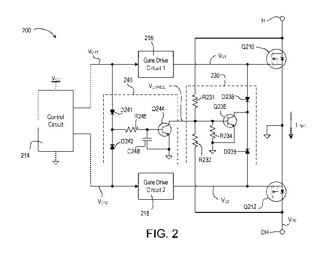
[0008] FIG. 2 is a simplified schematic diagram of another example load
control device
showing an overcurrent protection circuit and an override circuit.
[0009] FIG. 3 shows simplified waveforms that illustrate the operation of
the load control
device of FIG. 2.
DETAILED DESCRIPTION
[0010] FIG. 1 is a simplified block diagram of an example load control
device 100 (e.g., a
dimmer switch) for controlling the amount of power delivered to an electrical
load, such as, a
lighting load 102. The load control device 100 may have a hot terminal H
coupled to an
alternating-current (AC) power source 104 for receiving an AC mains line
voltage VAC, and a
dimmed-hot terminal DH coupled to the lighting load 102.
[0011] The load control device 100 may comprise a controllably conductive
device 110, such
as two field-effect transistors (FETs) Q112, Q114 that may be coupled in anti-
series connection
between the hot terminal and the dimmed-hot terminal DH. The junction of the
FETs may be
coupled to circuit common. The load control device 100 may comprise a control
circuit 115, e.g., a
digital control circuit, for controlling the FETs Q112, Q114 to conduct a load
current ILOAD through
the lighting load 102. The control circuit 115 may include one or more of a
processor (e.g., a
microprocessor), a microcontroller, a programmable logic device (PLD), a field
programmable gate
array (FPGA), an application specific integrated circuit (ASIC), or any
suitable controller or
processing device. The control circuit 115 may generate first and second drive
signals VDR1, VDR2
that may be coupled to the gates of the respective FETs Q112, Q114 via first
and second gate drive
circuits 116, 118, respectively, for generating gate voltages VG1, VG2 at the
gates of the FETs. For
example, the first and second gate voltages VG1, VG2 may be the inverse of the
respective drive
signals VDRi, VDR2. When the controllably conductive device 110 is rendered
conductive during the
CA 03066729 2019-12-09
WO 2018/227124 PCT/US2018/036714
- 5 -
positive half-cycles of the AC power source 104, the load current LOAD may be
conducted through
the drain-source channel of the first FET Q112 and the body diode of the
second FET Q114. When
the controllably conductive device 110 is rendered conductive during the
negative half-cycles of the
AC power source 104, the load current LOAD may be conducted through the drain-
source channel of
the second FET Q114 and the body diode of the first FET Q112.
[0012] The control circuit 115 may receive a zero-cross control signal
Vzc representative of
the zero-crossing points of the AC main line voltage of the AC power source
104 from a zero-cross
detect circuit 120. The control circuit 115 may be configured to render the
FETs Q112, Q114
conductive and/or non-conductive at predetermined times (e.g., at a firing
time or firing angle)
relative to the zero-crossing points of the AC waveform to generate a phase-
control voltage Vpo
using a phase-control dimming technique (e.g., a forward phase-control dimming
technique and/or a
reverse phase-control dimming technique). Examples of dimmers are described in
greater detail in
commonly-assigned U.S. Patent No. 7,242,150, issued July 10, 2007, entitled
DIMMER HAVING A
POWER SUPPLY MONITORING CIRCUIT; U.S. Patent No. 7,546,473, issued June 9,
2009,
entitled DIMMER HAVING A MICROPROCESSOR-CONTROLLED POWER SUPPLY; and
U.S. Patent No. 8,664,881, issued March 4, 2014, entitled TWO-WIRE DIMMER
SWITCH FOR
LOW-POWER LOADS, the entire disclosures of which are incorporated by reference
herein.
[0013] The load control device 100 may include a power supply 122. The
power supply 122
may generate a direct-current (DC) supply voltage Vcc for powering the control
circuit 115 and the
other low-voltage circuitry of the load control device 100. The power supply
100 may be coupled in
parallel with the series combination of the FETs Q112, Q114. The power supply
122 may be
configured to conduct a charging current through the lighting load 102 to
generate the DC supply
voltage Vcc.
[0014] The load control device 100 may further comprise an overcurrent
protection
circuit 130 that may be coupled across the series combination of the FETs
Q112, Q114 for receiving
the voltage developed across the FETs. The voltage developed across the series
combination of the
FETs Q112, Q114 may be a function of the magnitude of the load current koAD
and an on
resistance RDs-oN of the conducting FET as well as the forward voltage drop of
the body diode of the
non-conducting FET. Thus, the voltage developed across the controllably
conductive device 110
CA 03066729 2019-12-09
WO 2018/227124 PCT/US2018/036714
- 6 -
(e.g., across the series combination of the FETs Q112, Q114) may be
representative of the
magnitude of the load current 'LOAD. The overcurrent protection circuit 130
may be responsive to the
magnitude of the load current 'LOAD (e.g., responsive to the magnitude of the
voltage developed
across the controllably conductive device 110, which may indicate the
magnitude of the load
current 'LOAD). The overcurrent protection circuit 130 may be electrically
coupled to the gates of the
FETs Q112, Q114 for controlling the FETs Q112, Q114 in the event of an
overcurrent condition.
For example, the overcurrent protection circuit 130 may be configured to
control the magnitude of
the gate voltages VG1, VG2 to approximately zero volts by shorting gates of
the respective FET Q112,
Q114 to circuit common.
[0015] The control circuit 115 may be coupled to the overcurrent
protection circuit 130 for
enabling and disabling the overcurrent protection circuit 130. For example,
the control circuit 115
may generate an enable control signal VENABLE for enabling and disabling the
overcurrent protection
circuit 130. When the control circuit 115 is controlling the FETs Q112, Q114
using the forward
phase-control dimming technique, the control circuit 115 may be configured to
disable the
overcurrent protection circuit 130 while the controllably conductive device
110 is non-conductive
during each half-cycle of the AC power source 104 (e.g., when one of the FETs
Q112, Q114 is
rendered non-conductive to block the flow of the load current 'LOAD). The
overcurrent protection
circuit 130 may be disabled while the controllably conductive device 110 is
non-conductive during
each half-cycle to prevent the overcurrent protection circuit 130 from
tripping when the controllably
conductive device 110 is rendered conductive during each half-cycle (e.g., at
the firing time or firing
angle). After control circuit 115 control one of the FETs Q112, Q114 to render
the controllably
conductive device 100 conductive, the magnitude of the phase-control voltage
Vpc may transition
from approximately zero volts to approximately the magnitude of the AC mains
line voltage VAC
over a switching time period (e.g., a rise time period and/or a turn-on time
period). In addition, the
control circuit 115 may be configured to delay enabling the overcurrent
protection circuit 130 for a
delay time period after the time at which one of the FETs Q112, Q114 is
controlled to render the
controllably conductive device 110 conductive during each half-cycle, for
example, to allow the FET
to become fully conductive during the switching time period.
CA 03066729 2019-12-09
WO 2018/227124 PCT/US2018/036714
- 7 -
[0016] While the two FETs Q112, Q114 are shown in FIG. 1, the two FETs
may be replaced
by a single FET in a full-wave rectifier bridge. In such an implementation,
the control circuit 115
may generate a single drive voltage for producing a single gate voltage at the
gate of the FET in the
bridge. The overcurrent protection circuit 130 may be coupled across the FET
in the bridge and
would be responsive to the voltage across the FET and thus the current
conducted through the FET.
The overcurrent protection circuit 130 may be configured to remove the gate
voltage from the gate
of the FET in the event of an overcurrent condition. The control circuit 115
would be configured to
disable the overcurrent protection circuit when the FET is non-conductive
during each half-cycle in a
similar manner as described above.
[0017] FIG. 2 is a simplified schematic diagram of another example load
control device 200
(e.g., the load control device 100 shown in FIG. 1) for controlling the amount
of power delivered to
an electrical load, such as a lighting load (e.g., the lighting load 102).
FIG. 3 shows simplified
waveforms that illustrate the operation of the load control device 200. The
load control device 200
may comprise a controllably conductive device 210, for example, including two
FETs Q212, Q214
coupled in anti-series connection between a hot terminal H (e.g., that may be
coupled to an AC
power source) and a dimmed-hot terminal DH (e.g., that may be coupled to the
lighting load). The
junction of the FETs Q212, Q214 may be coupled to circuit common. The load
control device 200
may comprise a control circuit 215 (e.g., a digital control circuit)
configured to control the
FETs Q212, Q214 using a forward phase-control dimming technique to generate a
phase-control
voltage Vpc to be provided to the lighting load (e.g., a forward phase-control
voltage as shown in
FIG. 3) and conduct a load current ILDAD through the lighting load. The
control circuit 215 may
include one or more of a processor (e.g., a microprocessor), a
microcontroller, a programmable logic
device (PLD), a field programmable gate array (FPGA), an application specific
integrated circuit
(ASIC), or any suitable controller or processing device. The control circuit
215 may be powered
from a first supply voltage Vcci (e.g., approximately 3.3 volts or 5 volts),
which may be generated
by a power supply of the load control device 200 (e.g., the power supply 122
shown in FIG. 1).
[0018] The control circuit 215 may generate first and second drive
signals VDRi, VDR2 for
controlling the magnitude of the phase-control voltage to be approximately
equal to zero volts for a
non-conduction time period TNc at the beginning of each half-cycle and
approximately equal to the
CA 03066729 2019-12-09
WO 2018/227124 PCT/US2018/036714
- 8 -
magnitude of the AC line voltage for a conduction time period Tc0N at the end
of each half-cycle.
The control circuit 215 may be configured to drive the first drive signal VDR1
high (e.g., towards the
first supply voltage Vcci) to render the first FET Q212 non-conductive for the
non-conductive time
period TNc during the positive half-cycles, and to drive the second drive
signal VDR2 high (e.g.,
towards the first supply voltage Vcci) to render the first FET Q212 non-
conductive for the
non-conductive time period TNc during the negative half-cycles (e.g., as shown
in FIG. 3). The first
and second drive signals VDRi, VDR2 may be coupled to the gates of the
respective FETs Q212, Q214
via first and second gate drive circuits 216, 218, respectively, for
generating gate voltages VG1, VG2.
The first and second gate drive circuits 216, 218 may pull the gates of the
respective FETs Q212,
Q214 up towards a second supply voltage Vcc2 (e.g., approximately 12 volts)
when the respective
drive signals VDRi, VDR2 is driven low towards circuit common as shown in FIG.
3). The
FETs Q212, Q214 may be rendered conductive when the gate voltages VG1, VG2 are
driven above
rated gate threshold voltages of the FETs.
[0019] The load control device 200 may further comprise an overcurrent
protection
circuit 230 that may be coupled across the series combination of the FETs
Q212, Q214 for receiving
the voltage developed across the FETs. The overcurrent protection circuit 230
may comprise two
resistors R231, R232 that may be coupled across the series combination of the
FETs Q212, Q214.
The junction of the resistors R231, R232 may be coupled to circuit common
through a sense
resistor R234, such that the series combination of the first resistor R231 and
the sense resistor R234
may be coupled in parallel with the drain-source junction of the first FET
Q212 and the series
combination of the second resistor R232 and the sense resistor R234 may be
coupled in parallel with
the drain-source junction of the second FET Q214. The sense resistor R234 may
be coupled across
the base-emitter junction of a transistor Q236, e.g., an NPN bipolar junction
transistor (BJT). The
collector of the transistor Q236 may be coupled to the gate of the first FET
Q212 through a
diode D238 and to the gate of the second FET Q214 through a diode D239.
[0020] In the event of an overcurrent condition (e.g., if the magnitude
of the load
current ILOAD exceeds an overcurrent threshold) while the controllably
conductive device 210 is
conductive, the overcurrent protection circuit 230 may render the FETs Q212,
Q214 non-conductive.
For example, the overcurrent protection circuit 230 may render the
controllably conductive
CA 03066729 2019-12-09
WO 2018/227124 PCT/US2018/036714
- 9 -
device 210 non-conductive, for example, by controlling the magnitude of the
gate voltages VG1, VG2
towards circuit common (e.g., to a voltage less than the rated gate threshold
voltages of the FETs) to
render both of the FETs non-conductive. The overcurrent threshold may be set
such that the
overcurrent protection circuit 230 does not render the FETs Q212, Q214 non-
conductive during
normal operation (e.g., even during the conduction of an inrush current when
the lighting load is first
turned on). For example, the overcurrent threshold may be set such that the
overcurrent protection
circuit 230 renders the FETs Q212, Q214 non-conductive if the magnitude of the
load current 'LOAD
exceeds approximately 70 amps. In addition, the overcurrent protection circuit
230 may generate an
overcurrent feedback signal, which may indicate an overcurrent condition and
may be received by
the control circuit 215, and the control circuit may be configured to control
gate voltages VG1, VG2 to
render the FETs Q212, Q214 non-conductive in response to the overcurrent
feedback signal.
[0021] When the first FET Q212 is rendered conductive, the overcurrent
protection
circuit 230 may render both FETs non-conductive Q212, Q214 if the magnitude of
the load
current 'LOAD conducted through the first FET Q212 exceeds the overcurrent
threshold. The voltage
developed across the series combination of the first resistor R231 and the
sense resistor R234 may be
a function of the magnitude of the load current LOAD and an on resistance RDs-
oNi of the first
FET Q212 when the drain-source channel of the first FET Q212 is conducting the
load current 'LOAD.
When the magnitude of the load current LOAD increases during an overcurrent
condition, the voltage
developed across the first FET Q212 due to the on resistance RDs-oNi may
increase significantly.
Because the body diode of the second FET Q214 is coupled across the second
resistor R232 and the
sense resistor R234, the voltage developed across the second FET Q214 during
the overcurrent
condition does not appreciably affect the voltage developed across the sense
resistor R236. When
the magnitude of the load current LOAD exceeds the overcurrent threshold, the
voltage across the
sense resistor R234 may exceed a rated base-emitter voltage of the transistor
Q236, which may
render the transistor Q236 conductive. Accordingly, the gate of the first FET
Q212 may be pulled
down towards circuit common through the first diode D238 and the transistor
Q236, thus rendering
the first FET Q212 non-conductive. Since the first FET Q212 is non-conductive,
the voltage
developed across the FETs Q212, Q214 may be approximately equal to the AC
mains line
voltage VAC, which may maintain the transistor Q236 conductive and the first
FET Q212
CA 03066729 2019-12-09
WO 2018/227124 PCT/US2018/036714
- 10 -
non-conductive (e.g., until the magnitude of the AC mains line voltage VAC
drops to zero volts at the
next zero-crossing).
[0022] The overcurrent protection circuit 230 may operate in a similar
manner in response to
an overcurrent condition in the second FET Q214. The voltage developed across
the series
combination of the second resistor R232 and the sense resistor R234 may be a
function of the
magnitude of the load current 'LOAD and an on resistance RDs-oN2 of the second
FET Q214 when the
drain-source channel of the second FET Q214 is conducting the load current
'LOAD. When the
magnitude of the load current 'LOAD exceeds the overcurrent threshold, the
voltage developed across
the second FET Q214 due to the on resistance RDs-oN2 may increase
significantly, which may cause
the voltage across the sense resistor R234 to exceed the rated base-emitter
voltage of the
transistor Q236 and cause the transistor Q236 to be rendered conductive. The
gate of the second
FET Q214 may be pulled down towards circuit common through the second diode
D239 and the
transistor Q236, thus rendering the second FET Q214 non-conductive. Since the
second FET Q214
is non-conductive, the voltage developed across the FETs Q212, Q214 may be
approximately equal
to the AC mains line voltage VAC, which may maintain the transistor Q236
conductive and the
second FET Q214 non-conductive (e.g., until the magnitude of the AC mains line
voltage VAC drops
to zero volts at the next zero-crossing).
[0023] The control circuit 215 may be coupled to the overcurrent
protection circuit 230
through an override circuit 240 for enabling and disabling the overcurrent
protection circuit 230.
The override circuit 240 may receive the first and second drive signals VDRi,
VDR2 and may generate
an enable control signal VENABLE for enabling and disabling the overcurrent
protection circuit 230.
The override circuit 240 may comprise two diodes D241, D242 having anodes
coupled to receive the
first and second drive signals VDRi, VDR2, respectively, and cathodes coupled
together. The junction
of the diodes D241, D242 may be coupled to a base of a transistor Q244 (e.g.,
an NPN bipolar
junction transistor) through a resistor-capacitor (RC) circuit having a
resistor R246 and a
capacitor R248. The enable control signal VENABLE may be generated at the
collector of the
transistor Q244, which may be coupled to the base of the transistor Q236 of
the overcurrent
protection circuit 230. In addition, the control circuit 215 may generate the
enable control
signal VENABLE (e.g., at an output pin), such that the override circuit 240
may not be required.
CA 03066729 2019-12-09
WO 2018/227124 PCT/US2018/036714
- 11 -
[0024] When the first drive signal VDR1 or the second drive signal VDR2
is driven high
towards the supply voltage Vcc, the capacitor C248 may charge through the
respective diode D241,
D242 and the resistor R246. When the voltage across the capacitor C248 exceeds
the rated
base-emitter voltage of the transistor Q244, the transistor may be rendered
conductive, thus pulling
the enable control signal VENABLE down towards circuit common. When the enable
control
signal VENABLE is low, the transistor Q236 of the overcurrent protection
circuit 230 is prevented from
being rendered conductive, thus disabling the overcurrent protection circuit.
Since the first and
second drive signals VDR1, VDR2 are driven high to render the respective FET
Q212, Q214
non-conductive, the overcurrent protection circuit 230 is disabled when the
FETs Q212, Q214 are
non-conductive.
[0025] When one of the first and second drive signals VDR1, VDR2 is
driven low to render the
respective FET Q212, Q214 conductive, the overcurrent protection circuit 230
may be enabled after
a first delay period TDELAyi from when the respective drive signal is driven
low (e.g., as shown in
FIG. 3). For example, the RC circuit of the override circuit 240 may provide
the first delay
period TDELAyi (e.g., the time required for the capacitor C248 to discharge to
a point where the
voltage across the base-emitter junction of the transistor Q244 drops below
the rated base-emitter
voltage). The first delay period TDELAY1 may be, for example, approximately 60
microseconds,
which may be longer than a switching time period of the FETs Q212, Q214.
Similarly, the
overcurrent protection circuit 230 may be disabled after a second delay period
TDELAy2 (e.g.,
approximately 60 microseconds) from when one of the first and second drive
signals VDR1, VDR2 is
driven high to render the respective FET Q212, Q214 non-conductive.
[0026] If the control circuit 215 were to leave the overcurrent
protection circuit 230 enabled
when the controllably conductive device 210 is non-conductive (e.g., when one
or both of the
FETs Q212, Q214 are non-conductive) at the beginning of each half-cycle, the
voltage developed
across the controllably conductive device may be approximately equal to the AC
mains line
voltage VAC, which may cause the overcurrent protection circuit 230 to pull
the gate
voltages VG1, VG2 at the gates of the respective FETs Q212, Q214 down toward
circuit common. As
a result, the control circuit 215 would not be able to drive the gate voltages
VG1, VG2 above the rated
gate threshold voltages of the FETs Q212, Q214, and thus would not be able to
render the
CA 03066729 2019-12-09
WO 2018/227124 PCT/US2018/036714
- 12 -
FETs Q212, Q214 conductive at the firing time. Accordingly, the control
circuit 215 may be
configured to disable the overcurrent protection circuit 230 while the
controllably conductive
device 210 is non-conductive to prevent the overcurrent protection circuit 230
from controlling the
gate voltages VG1, VG2 of the FETs Q212, Q214 until after the controllably
conductive device is
rendered conductive at the firing time each half-cycle (e.g., until after the
first delay period TDELAY1).