Note: Descriptions are shown in the official language in which they were submitted.
CA 03067043 2019-12-11
WO 2018/232206
PCT/US2018/037697
TITLE
COATED ELECTROSURGICAL VESSEL SEALER ELECTRODES
CROSS-REFERENCE TO RELATED APPLICATIONS
[0001] The present application claims priority to U.S. Provisional App.
No.
62/520,126, filed on June 15, 2017.
BACKGROUND OF THE INVENTION
1. FIELD OF THE INVENTION
[0002] The present invention relates to electrosurgical vessel sealers
and, more
specifically, vessel sealing electrodes that are coated with a non-conducting
material to
provide the requisite gap distance between the electrodes.
2. DESCRIPTION OF THE RELATED ART
[0003] Electrosurgical vessel sealers are used for the occlusion of blood
vessels and
halting of bleeding during surgical procedures. The electrodes of the vessel
sealer are
interconnected to an electrosurgical generator that can selective supply
radiofrequency (RF)
energy to the electrodes for the desiccation and sealing of a blood vessel
that has been
clamped between the electrodes. A blade may be additionally incorporated into
the jaws for
cutting of the sealed blood vessel along an intermediate portion of the seal
created by the
energized electrodes.
[0004] For safe and effective operation, the electrodes of the vessel
sealer must
remain separated by approximately 0.002 to 0.006 inches (0.0508 to 0.1524
millimeters)
when clamping a blood vessel to prevent arcing or shorting when the electrodes
are
energized. As the blood vessel does not typically occupy the entire region
between the
electrodes, there is a constant risk that the electrodes will be allowed to
come into contact
with each other or become so closely positioned that arcing or shorting will
occur. Current
approaches for maintaining the appropriate electrode separate involve non-
conducting blocks
or stops that are positioned along the electrodes to physically prevent the
electrodes from
becoming too closely positioned relative to each other when energized. While
stops can
maintain the proper distance between the electrodes, they are difficult to
install and thus
increase the costs and complexity involved in the manufacturing of the vessel
sealer.
Accordingly, there is a need in the art for an approach that can ensure the
appropriate gap
between the electrodes of the vessel sealer without the need to form or place
physical stops
along the j aws.
1
CA 03067043 2019-12-11
WO 2018/232206 PCT/US2018/037697
BRIEF SUMMARY OF THE INVENTION
[0005] The present invention is a vessel sealing device that uses a non-
conductive
coating that is applied non-uniformly to the electrodes of the device to
maintain adequate
separation of the electrodes while allowing sufficient RF energy to pass
between the
electrodes to seal any vessel positioned therebetween. The vessel sealing
device comprises a
pair of electrodes that are moveable between open and closed positions and a
coating formed
from a non-conductive material applied non-uniformly to at least one of the
pair of electrodes
such that radiofrequency (RF) energy will only pass between the pair of
electrodes if a vessel
is positioned therebetween in contact with the pair of electrodes. The coating
may be applied
non-uniformly to both of the pair of opposing electrodes. The coating may be
applied non-
uniformly such that the coating on each of the pair of electrodes has a total
profile that varies
between -5.8 micrometers and 6.2 micrometers from a centerline average. The
coating may
be applied non-uniformly such that the coating on each of the pair of
electrodes has a
roughness profile that varies between -6.5 micrometers and 6.5 micrometers
from a centerline
average. The vessel sealing device may further comprise a series of grooves
formed in the
face of each of the opposing electrodes. The coating may vary in thickness
between the face
and the grooves formed in the face. The series of grooves of the face of each
of the opposing
electrodes may extend transversely to the longitudinal axis of the face of
each of the opposing
electrodes. The series of grooves of the face of each of the opposing
electrodes may be
oriented in a herringbone pattern. The face of each of the opposing electrodes
may extend
from two opposing side walls to an inner track. The coating may further extend
across at
least a portion of the side walls.
[0006] A method of making a vessel sealing device having a pair of
opposing
electrodes according to the present invention comprises texturing the face of
at least one of
the opposing electrodes and applying a non-conductive material non-uniformly
to the
textured face such that RF energy will only pass between the pair of
electrodes if a vessel is
positioned therebetween in contact with the pair of electrodes. The step of
texturing the face
of at least one of the opposing electrodes may comprise grit blasting the
face. The method
may further comprise the step of applying the non-conductive material to at
least one side
wall adjacent to the face of at least one of the opposing electrodes. The face
of the at least
one opposing electrode may include a groove formed therein and the step of
applying the
non-conductive material forms a coating that has a difference in thickness on
the face than in
the grooves.
2
CA 03067043 2019-12-11
WO 2018/232206
PCT/US2018/037697
BRIEF DESCRIPTION OF THE SEVERAL VIEWS OF THE DRAWING(S)
[0007] The present invention will be more fully understood and
appreciated by
reading the following Detailed Description in conjunction with the
accompanying drawings,
in which:
[0008] FIG. 1 is a perspective view of a vessel sealing system having
coated
electrodes according to the present invention;
[0009] FIG. 2 is perspective view of one electrode of a vessel sealing
system prior to
coating according to the present invention; and
[0010] FIG. 3 is perspective view of the preferred gap between two
electrodes of a
vessel sealing system prior to coating according to the present invention;
[0011] FIG. 4 is perspective view of one electrode of a vessel sealing
system that has
been coated according to the present invention;
[0012] FIG. 5 is perspective view of two electrodes of a vessel sealing
system that
have been coated according to the present invention;
[0013] FIG. 6 is a cross-section of two electrodes of a vessel sealing
system that have
been coated according to the present invention;
[0014] FIG. 7 is another cross-section of two electrodes of a vessel
sealing system
that have been coated according to the present invention; and
[0015] FIGS. 8 is a cross-section of an electrode edge profile for
controlling thinning
of a coating according to the present invention;
[0016] FIGS 9A and 9B are exemplary patterns for increasing the number of
current
flow paths according to the present invention;
[0017] FIG. 10 is an example of a herringbone groove pattern for a vessel
sealing
system according to the present invention;
[0018] FIG. 11 is a perspective view of a vessel sealing system having
uncoated
electrodes according to the present invention;
[0019] FIG. 12 is perspective view of one electrode of a vessel sealing
system having
coated electrodes according to the present invention;
[0020] FIG. 13 is side view of a vessel sealing system having uncoated
electrodes
according to the present invention;
[0021] FIG. 14 is side view of a vessel sealing system having coated
electrodes
according to the present invention;
[0022] FIG. 15 is cross-sectional view of two electrodes of a vessel
sealing system
that have been coated according to the present invention;
3
CA 03067043 2019-12-11
WO 2018/232206 PCT/US2018/037697
[0023] FIG. 16 is an example of a herringbone groove pattern for a vessel
sealing
system according to the present invention that cross-hatches with the
herringbone pattern of
FIG. 10; and.
[0024] FIG. 17 is an example of a transverse groove pattern for a vessel
sealing
system according to the present invention; and
[0025] FIG. 18 is a series of graphs of the surface topography of a
vessel sealing
system that has been coated according to the present invention.
DETAILED DESCRIPTION OF THE INVENTION
[0026] Referring to the figures, wherein like numerals refer to like
parts throughout,
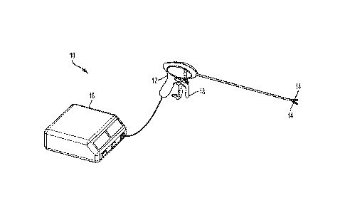
there is seen in FIG. 1 a vessel sealing system 10 comprising a vessel sealer
12 having a pair
of conductive opposing electrodes 14 that are interconnected to an
electrosurgical generator
16 that can supply RF energy to electrodes 14 for the desiccation of a blood
vessel trapped
between electrode 14. The dimensions of electrode 14 and the type of RF energy
supplied to
electrode 14 will produce desiccation of the blood vessel in a region of a
particular width as
determined by the thermal spread of the energy being supplied to the blood
vessel. As is
known in the art, electrode 14 may be held within non-conducting structures to
form jaws that
are hinged to allow electrode 14 to be open and closed in response to a user
operating a
handle 18 of sealer 12.
[0027] As seen in FIG. 2, each electrode 14 has a generally planar face
20 for
contacting the blood vessel that extends between two opposing sides 22 and 24
that define the
width of face 20. The transition between face 20 and sides 22 and 24 is
defined by a curved
edge 26 having a predetermined radius. Electrode 14 further includes a track
28 defined by
walls 30 and 32 extending from face 20. Walls 30 and 32 are spaced apart to
allow a cutting
instrument or knife (not shown) that may be disposed longitudinally in track
28 between both
electrode 14 to sever a blood vessel within the region of thermal spread
formed by the
application of RF energy from the electrode 14 to the blood vessel. The
intersection of walls
30 and 32 with face 20 defines a pair of opposing corners 34 and 36, shown in
FIG. 2 as
being substantially perpendicular.
[0028] Referring to FIG. 3, when electrode 14 are closed, they must
remain separated
by a specified distance d to prevent arcing or shorting when the RF energy is
supplied by
generator 16. As seen in FIG. 4, the required distance d may controlled via a
coating 38
applied to at least one electrode 14 and, preferably, both electrode 14. As
seen in FIG. 5,
coating 38 may be applied to both electrode 14 so that the total thicknesses
ti and t2 of coating
38 produces distanced, such as that seen in FIG. 6 and 7. While thickness ti
and t2 of coating
4
CA 03067043 2019-12-11
WO 2018/232206 PCT/US2018/037697
38 on electrode 14 is depicted in FIGS. 6 and 7 as generally the same, it
should be recognized
that coating of one electrode 14 may be thicker or thinner than the other
electrode 14,
providing that the sum of thicknesses ti and t2 produce the desired distance d
between
electrode 14. For example, to obtain distance d of between 0.002 to 0.006
inches (0.0508 to
0.1524 millimeters), coating 38 may be applied to each electrode 14 to
thickness of between
0.001 to 0.003 inches (0.0254 to 0.0762 millimeters).
[0029] Coating 38 may comprise a non-conductive material such as Teflon
(polytetrafluoroethylene/PTFE), ElectroBond (silicone epoxy), silicone rubber
(polydimethylsiloxane), high temperature paints such as Thurmalox 282
Stainless Steel
paint, as well as ceramic coatings, glass based coatings, liquid crystal
polymers, and high
temperature engineering amorphous and semi-crystalline thermoplastics such as
polysulfone
(PSU), polyethersulfone (PES), polyphenylsulfone (PPSU), polytherimide (PEI),
polyamide-
imide (PAI), polyphthalamide (PPA), polyphenylene sulfide (PPS), and
polyetheretherketone
(PEEK). Coating 38 may be applied to electrode 14 via electrostatic spraying,
fluid bed
coating, plasma spray coating, and other conventional processes. Coating 38
may comprise a
single layer applied at one or multiple layers applied by repeating the
coating process.
Coating 38 may additionally comprise multiple layers of different materials.
It should be
recognized that the non-conductive material selected for coating 38 and used
to form distance
d may provide additional benefits, such as a non-stick surface that reduces
adhesion between
electrode 14 and the blood vessel being desiccated.
[0030] Referring to FIG. 7, coating 38 does not have a uniform thickness
across the
entire electrode 14. Instead, upper and lower electrode 14 have corresponding
regions r1 and
r2 proximate to corners 34 and 36 where the thickness of coating 38 is reduced
relative to the
thicknesses of coating 38 proximately to face 20 and walls 30 and 32. The
reduced thickness
regions r1 and r2 may be controlled by the profile of walls 30 and 32 defining
track 28. For
example, as seen in FIG. 7, walls 30 and 32 connect to the respective faces 20
of electrode 14
at substantially right angles. Due to this angular profile, i.e., the edge
formed by the
intersection of walls 30 and 32 with face 20, coating 38 will be thinner when
deposited on
electrode 14 due to the surface tension of the molecules of coating 38 in
combination with the
composition of the substrate, i.e., face 20, the surrounding air, and the
temperature of all
components. Referring to FIG. 8, the geometry of the edge formed by the
intersection of
walls 30 and 32 with face 20 may be varied to control the dimension of reduced
thickness
regions r1 and r2, such as through the use of a more acute angle, a bevel, a
small radius curve,
or other geometric feature that reduces the thickness of coating 38
proximately to corners 34
CA 03067043 2019-12-11
WO 2018/232206 PCT/US2018/037697
and 36. Some radius may be allowable, but generally the sharper the angle the
more thinning
will occur. For example, a corner sharper than 90 degrees is likely to thin
the coating even
more, as seen in FIG. 8. Gravity may also be used thin the coating during
application. If
corners 34 and 36 are pointed upwardly during coating, gravity will augment
the contact
angle effect in thinning coating 38 at the edge.
[0031] While the dimensions of reduced thickness regions r1 and r2 may
vary slightly
based on the particular material chosen for coating 38, reduced thickness
regions r1 and r2
should be thinner than thicknesses ti and t2 of coating 38 positioned
proximately to the
remaining portions of electrode 14. For example, when coating 38 comprises
silicone epoxy
and PTFE and thicknesses ti and t2 are 0.001 to 0.003 inches (0.0254 to 0.076
millimeters),
reduced thickness regions r1 and r2 must be less than .001 inches (0.0254
millimeters) thick.
For PTFE (600 V/mil dielectric strength) with an electrosurgical generator 16
that outputs
200 volts peak, r1 <200 V / 600 V/mil = .00033 inches (0.0084 millimeters). It
should be
recognized that these dimensions, as well as distance d, may vary from the
exemplary
dimensions are ultimately dependent on the intended use of system 10, such as
the amount of
RF energy being supplied and the effect system 10 is intended to have on the
target tissues,
and thus could be varied depending on the particular circumstances.
[0032] The reduced thickness regions r1 and r2 of the present invention
allow for the
flow of RF energy between electrode 14 despite the non-conductive material
used of coating
38. As a result, RF energy is allowed to flow between electrode 14 at the
locations where
reduced thickness region r1 of one electrode 14 is positioned opposite from
reduced thickness
region r2 of the other electrode 14, i.e., desiccation occurs along track 28.
This localization of
RF energy transfer has the added benefit of more narrowly constraining the
thermal spread in
the target blood vessel and thus provide for improved control over the region
where
desiccation occurs in the blood vessel. Referring to FIGS. 9A and 9B, face 20
of electrode 14
may be patterned to increase the number of current flow paths by increasing
the number of
angular surfaces or edges formed by face 20 and thus increasing the number of
locations
where the thinning of coating occurs.
[0033] Referring to FIG. 11, face 20 of electrode 14 may include a series
of grooves
40 formed in a herringbone pattern to increase the number of locations having
reduced
thickness, i.e., reduced thickness regions r1 and r2 will form along the
opposing edges 42 and
44 that define grooves 40 in addition to corners 34 and 36 of track 28. Face
20 of an
opposing electrode 14 may be similarly patterned to correspond, either with a
herringbone
pattern that has grooves 40 that substantially align with the first electrode
14 or a herringbone
6
CA 03067043 2019-12-11
WO 2018/232206 PCT/US2018/037697
pattern oriented in the opposite direction of grooves of first electrode 14 so
that grooves 40 of
one electrode 14 form a cross-hatching pattern with grooves of the other
electrode 14 when
they are positioned against each other.
[0034] In another aspect, the invention comprises a vessel sealing system
110
comprising a vessel sealer 112 having a pair of conductive electrodes 114 that
are positioned
in opposing jaws 116 and that may be interconnected to an electrosurgical
generator (not
shown) that selectively supplies RF energy to electrodes 114 for the
desiccation of a blood
vessel trapped between electrode 114. The dimensions of electrodes 114 and the
type of RF
energy supplied to electrodes 114 produce desiccation of the blood vessel in a
region of a
particular width may be determined by the thermal spread of the energy being
supplied to the
blood vessel. As is known in the art, electrodes 114 may be held within non-
conducting jaws
116 that are hinged to allow two opposing electrodes 114 to be open and closed
in response
to a user operating a handle or trigger associated with sealer 112.
[0035] Each electrode 114 has a generally planar face 120 for contacting
the blood
vessel that extends between two opposing sides 122 and 124 that define the
width of face
120. The transition between face 120 and sides 122 and 124 is defined by a
curved edge 126
having a predetermined radius. Electrode 114 further includes a track 128
defined by walls
130 and 132 extending from face 120. Walls 130 and 132 are spaced apart to
allow a cutting
instrument or knife (not shown) that may be longitudinally extended and
retraced along
tracks 128 of both electrodes 114 to sever a blood vessel within the region of
thermal spread
formed by the application of RF energy from the electrode 114 to the blood
vessel. The
intersection of walls 130 and 132 with face 120 defines a pair of opposing
corners 134 and
136, shown in FIG. 12 as being substantially perpendicular.
[0036] Referring to FIG. 12, when jaws 116 are closed, opposing
electrodes 114 must
remain separated by a specified distance d to prevent arcing or shorting when
the RF energy
is supplied by the external generator. As seen in FIG. 13, the required
distance d may
controlled via a non-uniform coating 138 applied to at least one of the
opposing electrodes 14
and, preferably, both of the opposing electrodes 114, so that energy can flow
between
opposing electrodes 114 despite the present of non-uniform coating 138. Non-
uniform
coating 138 is applied to one or both electrodes 14 so that the total
thicknesses ti and t2 of
coating 38 produces distance d. While thickness ti and t2 of non-uniform
coating 138 on each
electrode 114, respectively, may the same, it should be recognized that non-
uniform coating
138 of one electrode 14 may be thicker or thinner than non-uniform coating 138
of the other
electrode 14, providing that the sum of thicknesses ti and t2 produce the
desired distance d
7
CA 03067043 2019-12-11
WO 2018/232206 PCT/US2018/037697
between electrode 14. The thickness of non-uniform coating 138 on each of
opposing
electrodes 114 when applied to both of opposing electrodes 114, may be between
0.0005
inches (0.0127 millimeters) and 0.002 inches (0.0508 millimeters,) with a
preferred thickness
of 0.001 inches (0.0254 millimeters).
[0037] Regardless of thickness, non-uniform coating 138 should be
sufficient to
prevent the flow of RF energy between opposing electrodes 114 during normal
operating
conditions if a vessel is not positioned therebetween. If a vessel is present,
however, the non-
uniformity of non-uniform coating 138 allows the vessel to contact enough of
the uncoated or
very thinly coated portions of electrodes 114 so that RF energy may flow
between the
electrodes 114 via the vessel despite the non-conductivity of the material
used for coating
138. As a result, RF energy that flows between electrodes 114 will produce
desiccation of
any vessel trapped therebetween. Non-uniform coating 138 thus provides for a
predetermined amount of RF energy to pass through an entrapped vessel for
desiccation of
the vessel tissue positioned between electrodes 114 when RF energy is applied
while
maintaining a sufficient gap distance between electrodes 114 to prevent arcing
or shorting
under normal conditions when no vessel is present. While non-uniform coating
138 can
theoretically allow energy flow under extreme conditions, e.g., enough RF
energy to ionize
the air so that it becomes conductive, the purpose of non-uniform coating 138
is to prevent
flow during the operating conditions that system 10 can actually experience
when a vessel is
not positioned between the electrodes and to allow energy to flow when a
vessel is clamped
between the electrodes under reasonable operating conditions available to
conventional RF
generators and in amounts that are useful for electrosurgical operations. For
example, non-
uniform coating 138 may be applied in a manner such that the pair of opposing
electrodes
have approximately 400 ohm of starting resistance in a constant power mode of
20-100 Watts
with a voltage of 80-160 Vrms when positioned around and in contact with an
exemplary
vessel. Thus, one embodiment may have 400 ohm of starting resistance in a
constant power
mode of 25 Watts with a voltage of 100 volts when positioned around and in
contact with a
vessel. The appropriate resistance may be accomplished by using non-uniform
coating 138 to
produce a gap of more than .001 inches between the electrodes. Thus, non-
uniform coating
138 may have a total thickness of .0008 inches .0002 inches, so when applied
to both
electrodes 114, the total thickness and thus gap distance will be slightly
below .0020 inches
but still effective in preventing shorting or arcing when a vessel is not
positioned between
electrodes 114. It should be recognized that power levels may need to vary
with the size of
electrodes 114 and with different overall thicknesses of non-uniform coating
138. For
8
CA 03067043 2019-12-11
WO 2018/232206 PCT/US2018/037697
example, an acceptable non-uniform coating 138 can vary in starting impedance
from as high
as around 600-800 ohm to as low as 150 or 200 ohm depending on the thickness
of non-
uniform coating 138.
[0038] Non-uniform coating 138 may comprise a non-conductive material such
as
Teflon (polytetrafluoroethylene/PTFE), ElectroBond (silicone epoxy), silicone
rubber
(polydimethylsiloxane), high temperature paints such as Thurmalox 282
Stainless Steel
paint, as well as ceramic coatings, glass based coatings, liquid crystal
polymers, and high
temperature engineering amorphous and semi-crystalline thermoplastics such as
polysulfone
(PSU), polyethersulfone (PES), polyphenylsulfone (PPSU), polytherimide (PEI),
polyamide-
imide (PAT), polyphthalamide (PPA), polyphenylene sulfide (PPS), and
polyetheretherketone
(PEEK). It should be recognized that the non-conductive material selected for
coating 138
and used to form distance d may provide additional benefits, such as a non-
stick surface that
reduces adhesion between electrode 114 and the blood vessel being desiccated.
[0039] Referring to FIG. 15, non-uniform coating 138 is provided across
each
electrode 114, beginning with a portion of the two opposing sides 122 and 124
that define the
width of face 120 and extending over curved edge 126 at the transition between
sides 122 and
124 and face 120. Coating 138 extends across the planar surface of face 120,
the pair of
opposing corners 134 and 136, and walls 130 and 132 that define track 128.
[0040] As further seen in FIG. 16, face 120 may include grooves 140 or
other
topological features that are also covered with coating 138. For example, as
seen in FIG. 16,
face 120 includes a plurality of grooves 140 arranged in a herringbone
pattern. Face 120 of
an opposing electrode 114 may be similarly patterned to correspond, either
with a
herringbone pattern that has grooves 140 that substantially align with the
first electrode 114
or a herringbone pattern oriented in the opposite direction of grooves of
first electrode 114 so
that grooves 140 of one electrode 114, such as that seen in FIG. 10, to form a
cross-hatching
pattern with grooves 40 of the other electrode 114 when electrodes 114 are
positioned against
each other. Referring to FIG. 17, grooves 140 may also extend transversely
across electrodes
114 so that grooves 140 are perpendicular to the longitudinal axis of face
120.
[0041] Non-uniform coating 138 is created by performing a thermal burn off
and then
grit blasting of the uncoated electrodes 114 to form a roughened topological
surface on
electrodes 114. Electrodes 114 are then masked and coated with the coating
material to form
non-uniform coating 138. The coated electrodes 114 are thermally cured in an
oven and
inspected.
9
CA 03067043 2019-12-11
WO 2018/232206 PCT/US2018/037697
[0042] As seen in FIG. 18, the face of an electrode 114 that has been
prepared and
coated non-uniformly with a non-conductive material according to the present
invention so
that the coated electrode 114 has non-uniform topological surface with regions
of relatively
thickly applied coating interspersed with regions that are not coated or very
thinly coated. It
should be recognized that the amount of non-uniformity may be varied to adjust
and control
the ability of the electrode 114 to conduct RF energy therebetween when a
vessel is in contact
with the non-uniform surface such that portions of the vessel come into
contact with the
uncoated or thinly coated regions. Thus, the more thickly coated regions serve
to provide
spacing between electrodes 114 to prevent arcing or shorting when a vessel is
not present,
and the very thinly or uncoated regions allow for conductivity when a vessel
comes into
contact with those regions and completes the circuit. The amount of non-
uniformity may be
controlled by varying the amount of grit blasting, the amount and thickness of
non-
conductive material applied to the grit-blasted face, and the particular non-
conductive
material used. In the example of FIG. 18, the surface of face 120 has a total
profile that
varies between -5.8 micrometers and 6.2 micrometers from the centerline
average, and a
roughness profile that varies between -6.5 micrometers and 6.5 micrometers
from the
centerline average. In an example, the percentage of electrodes 114 that are
exposed by non-
uniform application of the coating is around 1.5% of the non-uniformly coated
area.
[0043] In a first aspect, the invention is an electrode for a vessel
sealing device,
comprising a face extending along a planar surface, a pair of opposing walls
extending from
the face at a pair of opposing corners to define a knife track between the
pair of opposing
walls, and a non-conductive coating covering at least a portion of the face,
the pair of
opposing walls, and the opposing corners.
[0044] In a second aspect, the coating has a first thickness proximately
to the face and
the opposing walls and a second thickness that is less than the first
thickness proximately to
the pair of opposing corners.
[0045] In a third aspect, the second thickness is less than the first
thickness.
[0046] In a fourth aspect, the first thickness is between 0.001 to 0.006
inches (0.025
to 0.152 millimeters).
[0047] In a fifth aspect, the first thickness is between 0.001 and 0.003
inches (0.025
to 0.0762 millimeters).
[0048] In a sixth aspect, the non-conductive coating is selected from the
group
consisting of polytetrafluoroethylene (PTFE), silicone epoxy, silicone rubber,
polysulfone
(PSU), polyethersulfone (PES), polyphenylsulfone (PPSU), polytherimide (PEI),
polyamide-
CA 03067043 2019-12-11
WO 2018/232206 PCT/US2018/037697
imide (PAT), polyphthalamide (PPA), polyphenylene sulfide (PPS), and
polyetheretherketone
(PEEK).
[0049] In a seventh aspect, the invention may be a vessel sealing device,
comprising a
pair of jaws, wherein each jaw has an electrode with a face extending along a
planar surface
and a pair of opposing walls extending from the face at a pair of opposing
corners to define a
knife track between the pair of opposing walls, and a non-conductive coating
covering at a
minimum the face, the pair of opposing walls, and the opposing corners of each
electrode.
[0050] In an eighth aspect, the coating has a first thickness proximately
to the face
and the opposing walls and a second thickness that is less than the first
thickness proximately
to the pair of opposing corners.
[0051] In a ninth aspect, the second thickness is less than the first
thickness.
[0052] In a tenth aspect, the first thickness is between 0.001 and 0.003
inches (0.025
to 0.0762 millimeters).
[0053] In an eleventh aspect, the non-conductive coating is selected from
the group
consisting of is selected from the group consisting of polytetrafluoroethylene
(PTFE),
silicone epoxy, silicone rubber, polysulfone (PSU), polyethersulfone (PES),
polyphenylsulfone (PPSU), polytherimide (PEI), polyamide-imide (PAT),
polyphthalamide
(PPA), polyphenylene sulfide (PPS), and polyetheretherketone (PEEK).
11