Note: Descriptions are shown in the official language in which they were submitted.
CA 03067149 2019-12-11
WO 2019/018112
PCT/US2018/039992
WAVEFORM DESIGN BASED ON POWER SPECTRAL
DENSITY (PSD) PARAMETERS
CROSS REFERENCE TO RELATED APPLICATIONS
[0001] The present application claims priority to and the benefit of the U.S.
Nonprovisional
Patent Application No. 16/020,400, filed June 27, 2018, and U.S. Provisional
Patent
Application No. 62/535,098, filed July 20, 2017, which are hereby incorporated
by reference
in their entirety as if fully set forth below and for all applicable purposes.
TECHNICAL FIELD
[0002] This application relates to wireless communication systems and methods,
and more
particularly to communicating in a frequency spectrum using interlaced
frequency channels
and non-interlaced frequency channels based on power spectral density (PSD)
parameters.
INTRODUCTION
[0003] Wireless communications systems are widely deployed to provide various
types of
communication content such as voice, video, packet data, messaging, broadcast,
and so on.
These systems may be capable of supporting communication with multiple users
by sharing
the available system resources (e.g., time, frequency, and power). A wireless
multiple-access
communications system may include a number of base stations (BSs), each
simultaneously
supporting communication for multiple communication devices, which may be
otherwise
known as user equipment (UE).
[0004] To meet the growing demands for expanded mobile broadband connectivity,
wireless
communication technologies are advancing from the LTE technology to a next
generation
new radio (NR) technology. NR may provision for dynamic medium sharing among
network
operators in a licensed spectrum, a shared spectrum, and/or an unlicensed
spectrum. For
example, shared spectrums and/or unlicensed spectrums may include frequency
bands at
about 3.5 gigahertz (GHz), about 6 GHz, and about 60 GHz.
[0005] Some shared spectrums and/or unlicensed spectrums may have certain PSD
requirements. For example, the European Telecommunications Standard Institute
(ETSI)
document EN 301 893 V2.1.1 specifies various PSD limits for sub-6 GHz
frequency bands
1
CA 03067149 2019-12-11
WO 2019/018112
PCT/US2018/039992
and the ETSI draft document EN 302 567 V2Ø22 specifies a maximum equivalent
isotropic
radiated power (EIRP) and an EIRP density for 60 GHz frequency bands. Some
other
frequency bands, such as citizens broadband radio service (CBRS) bands at
about 3.5 GHz,
may not restrict transmissions to a particular PSD limit. In general,
different spectrums may
have different PSD requirements and/or different bandwidth occupancy
requirements. Thus,
during spectrum sharing, transmissions in such shared spectrums and/or
unlicensed spectrums
are required to meet PSD requirements and/or frequency occupancy requirements
of
corresponding spectrums.
BRIEF SUMMARY OF SOME EXAMPLES
[0006] The following summarizes some aspects of the present disclosure to
provide a basic
understanding of the discussed technology. This summary is not an extensive
overview of all
contemplated features of the disclosure, and is intended neither to identify
key or critical
elements of all aspects of the disclosure nor to delineate the scope of any or
all aspects of the
disclosure. Its sole purpose is to present some concepts of one or more
aspects of the
disclosure in summary form as a prelude to the more detailed description that
is presented
later.
[0007] For example, in an aspect of the disclosure, a method of wireless
communication
including selecting, by a first wireless communication device, a waveform
structure between
an interlaced frequency structure and a non-interlaced frequency structure for
communicating
in a frequency spectrum; and communicating, by the first wireless
communication device
with a second wireless communication device in the frequency spectrum, a
communication
signal based on the selected waveform structure.
[0008] In an additional aspect of the disclosure, an apparatus including means
for selecting a
waveform structure between an interlaced frequency structure and a non-
interlaced frequency
structure for communicating in a frequency spectrum; and means for
communicating, with a
second wireless communication device in the frequency spectrum, a
communication signal
based on the selected waveform structure.
[0009] In an additional aspect of the disclosure, a computer-readable medium
having program
code recorded thereon, the program code including code for causing a first
wireless
communication device to select a waveform structure between an interlaced
frequency
structure and a non-interlaced frequency structure for communicating in a
frequency
spectrum; and code for causing the first wireless communication device to
communicate, with
2
CA 03067149 2019-12-11
WO 2019/018112
PCT/US2018/039992
a second wireless communication device in the frequency spectrum, a
communication signal
based on the selected waveform structure.
[0010] Other aspects, features, and embodiments of the present invention will
become
apparent to those of ordinary skill in the art, upon reviewing the following
description of
specific, exemplary embodiments of the present invention in conjunction with
the
accompanying figures. While features of the present invention may be discussed
relative to
certain embodiments and figures below, all embodiments of the present
invention can include
one or more of the advantageous features discussed herein. In other words,
while one or more
embodiments may be discussed as having certain advantageous features, one or
more of such
features may also be used in accordance with the various embodiments of the
invention
discussed herein. In similar fashion, while exemplary embodiments may be
discussed below
as device, system, or method embodiments it should be understood that such
exemplary
embodiments can be implemented in various devices, systems, and methods.
BRIEF DESCRIPTION OF THE DRAWINGS
[0011] FIG. 1 illustrates a wireless communication network according to
embodiments of the
present disclosure.
[0012] FIG. 2 is a block diagram of an exemplary user equipment (UE) according
to
embodiments of the present disclosure.
[0013] FIG. 3 is a block diagram of an exemplary base station (BS) according
to
embodiments of the present disclosure.
[0014] FIG. 4 illustrates a frequency interlacing scheme according to
embodiments of the
present disclosure.
[0015] FIG. 5 illustrates a frequency interlacing scheme according to
embodiments of the
present disclosure.
[0016] FIG. 6 illustrates a band-dependent waveform selection scheme according
to
embodiments of the present disclosure.
[0017] FIG. 7 is a signaling diagram of a network-specific waveform selection
method
according to embodiments of the present disclosure.
[0018] FIG. 8 is a signaling diagram of a UE-specific waveform selection
method according
to embodiments of the present disclosure.
[0019] FIG. 9 illustrates a random access transmission scheme according to
embodiments of
the present disclosure.
3
CA 03067149 2019-12-11
WO 2019/018112
PCT/US2018/039992
[0020] FIG. 10 illustrates a random access transmission scheme according to
embodiments of
the present disclosure.
[0021] FIG. 11 illustrates a frequency interlacing scheme with a reduced
subcarrier spacing
(SCS) according to embodiments of the present disclosure.
[0022] FIG. 12 is a flow diagram of a communication method with a waveform
selection
according to embodiments of the present disclosure.
DETAILED DESCRIPTION
[0023] The detailed description set forth below, in connection with the
appended drawings, is
intended as a description of various configurations and is not intended to
represent the only
configurations in which the concepts described herein may be practiced. The
detailed
description includes specific details for the purpose of providing a thorough
understanding of
the various concepts. However, it will be apparent to those skilled in the art
that these
concepts may be practiced without these specific details. In some instances,
well-known
structures and components are shown in block diagram form in order to avoid
obscuring such
concepts.
[0024] The techniques described herein may be used for various wireless
communication
networks such as code-division multiple access (CDMA), time-division multiple
access
(TDMA), frequency-division multiple access (FDMA), orthogonal frequency-
division
multiple access (OFDMA), single-carrier FDMA (SC-FDMA) and other networks. The
terms
"network" and "system" are often used interchangeably. A CDMA network may
implement a
radio technology such as Universal Terrestrial Radio Access (UTRA), cdma2000,
etc. UTRA
includes Wideband CDMA (WCDMA) and other variants of CDMA. cdma2000 covers IS-
2000, IS-95 and IS-856 standards. A TDMA network may implement a radio
technology such
as Global System for Mobile Communications (GSM). An OFDMA network may
implement
a radio technology such as Evolved UTRA (E-UTRA), Ultra Mobile Broadband
(UMB),
IEEE 802.11 (Wi-Fi), IEEE 802.16 (WiMAX), IEEE 802.20, Flash-OFDMA, etc. UTRA
and
E-UTRA are part of Universal Mobile Telecommunication System (UMTS). 3GPP Long
Term Evolution (LTE) and LTE-Advanced (LTE-A) are new releases of UMTS that
use E-
UTRA. UTRA, E-UTRA, UMTS, LTE, LTE-A and GSM are described in documents from
an organization named "3rd Generation Partnership Project" (3GPP). CDMA2000
and UMB
are described in documents from an organization named "3rd Generation
Partnership Project
4
CA 03067149 2019-12-11
WO 2019/018112
PCT/US2018/039992
2" (3GPP2). The techniques described herein may be used for the wireless
networks and radio
technologies mentioned above as well as other wireless networks and radio
technologies, such
as a next generation (e.g., 5th Generation (5G) operating in mmWave bands)
network.
[0025] The present application describes mechanisms for communicating in a
frequency
spectrum using interlaced frequency structure and non-interlaced frequency
structure based
on power spectral density (PSD) parameters. The PSD parameters may be
associated with a
maximum PSD level or a range of PSD levels allowable in the frequency
spectrum, a target
transmit PSD level, and/or a power utilization factor of a transmitter. An
interlaced frequency
structure may include multiple sets of interlacing frequency bands. For
example, a
transmission signal may be transmitted in a set of frequency bands spaced
apart from each
other and interlaced with another set of frequency bands. The distribution of
a transmit signal
in a frequency domain can reduce the transmit PSD of the signal. For example,
a frequency
occupancy distribution factor of about 5 may allow a transmitter to increase
the transmit
power by about 7 decibels (dB) while maintaining the same PSD level. Thus, the
distribution
in the frequency domain can improve power utilization. The disclosed
embodiments may
further improve power utilization by employing time domain repetitions (e.g.,
increasing a
transmission duration) in conjunction with frequency interlacing. The
disclosed embodiments
may further improve power utilization by reducing a SCS in conjunction with
frequency
interlacing to allow for a greater frequency distribution.
[0026] In an embodiment, the selection between an interlaced frequency
structure and a non-
interlaced frequency structure may be band-dependent. For example, a BS or a
UE may
select an interlaced frequency structure when communicating in a frequency
band with a PSD
requirement. Alternatively, a BS or a UE may select a non-interlaced frequency
structure
when communicating in a frequency band without a PSD requirement. The BS and
the UE
may have prior knowledge of the PSD requirements in various frequency bands
prior to
communicating in the frequency bands.
[0027] In an embodiment, the selection between an interlaced frequency
structure and a non-
interlaced frequency structure may be network-specific. For example, a BS may
signal an
interlaced frequency structure for a frequency band with a PSD requirement.
Alternatively, a
BS may signal a non-interlaced frequency structure for a frequency band
without a PSD
requirement. The signaling may be a broadcast signal to all UEs in a network.
[0028] In an embodiment, the selection between an interlaced frequency
structure and a non-
interlaced frequency structure may be UE-specific. For example, a BS may
configure a
CA 03067149 2019-12-11
WO 2019/018112
PCT/US2018/039992
power-limited UE with an interlaced frequency structure and configure a non-
power-limited
UE with a non-interlaced frequency structure. The configuration may be carried
in a radio
resource configuration (RRC) message.
[0029] In an embodiment, a BS may configure some random access resources with
an
interlaced frequency structure and some other random access resources with a
non-interlaced
frequency structure. A UE may choose to send a random access channel (RACH)
preamble
with the interlaced or non-interlaced random access resources based on a
downlink pathloss
measurement. In addition, the UE may perform power ramping in a random access
procedure
between the interlaced and non-interlaced RACH resources. For example, the UE
may begin
with transmitting a random access signal using a non-interlaced frequency
resource with an
initial transmit power. The UE may increase the transmit power for subsequent
random
access signal transmissions. The UE may switch to use an interlaced frequency
resource
when the transmit power is increased to a level exceeding a maximum PSD level
allowable in
a frequency band of the non-interlaced frequency resources.
[0030] Aspects of the present application can provide several benefits. For
example, the use
of frequency interlacing may improve power utilization at a transmitter. The
band-dependent,
network-specific, and/or UE-specific selections allow dynamic multiplexing of
interlaced
frequency channels and non-interlaced frequency channels based on PSD
requirements and
UEs' power utilization factors. The use of TTI bundling and/or reduced SCS
provides
flexibility in scheduling with power utilization consideration. The disclosed
embodiments
may be suitable for use in any wireless communication network with any
wireless
communication protocol.
[0031] FIG. 1 illustrates a wireless communication network 100 according to
embodiments of
the present disclosure. The network 100 includes BSs 105, UEs 115, and a core
network 130.
In some embodiments, the network 100 operates over a shared spectrum. The
shared
spectrum may be unlicensed or partially licensed to one or more network
operators. Access
to the spectrum may be limited and may be controlled by a separate
coordination entity. In
some embodiments, the network 100 may be a LTE or LTE-A network. In yet other
embodiments, the network 100 may be a millimeter wave (mmW) network, a new
radio (NR)
network, a 5G network, or any other successor network to LTE. The network 100
may be
operated by more than one network operator. Wireless resources may be
partitioned and
arbitrated among the different network operators for coordinated communication
between the
network operators over the network 100.
6
CA 03067149 2019-12-11
WO 2019/018112
PCT/US2018/039992
[0032] The BSs 105 may wirelessly communicate with the UEs 115 via one or more
BS
antennas. Each BS 105 may provide communication coverage for a respective
geographic
coverage area 110. In 3GPP, the term "cell" can refer to this particular
geographic coverage
area of a BS and/or a BS subsystem serving the coverage area, depending on the
context in
which the term is used. In this regard, a BS 105 may provide communication
coverage for a
macro cell, a pico cell, a femto cell, and/or other types of cell. A macro
cell generally covers
a relatively large geographic area (e.g., several kilometers in radius) and
may allow
unrestricted access by UEs with service subscriptions with the network
provider. A pico cell
may generally cover a relatively smaller geographic area and may allow
unrestricted access
by UEs with service subscriptions with the network provider. A femto cell may
also
generally cover a relatively small geographic area (e.g., a home) and, in
addition to
unrestricted access, may also provide restricted access by UEs having an
association with the
femto cell (e.g., UEs in a closed subscriber group (CSG), UEs for users in the
home, and the
like). A BS for a macro cell may be referred to as a macro BS. A BS for a pico
cell may be
referred to as a pico BS. A BS for a femto cell may be referred to as a femto
BS or a home
BS. In the example shown in FIG. 1, the BSs 105a, 105b and 105c are examples
of macro
BSs for the coverage areas 110a, 110b and 110c, respectively. The BSs 105d is
an example
of a pico BS or a femto BS for the coverage area 110d. As will be recognized,
a BS 105 may
support one or multiple (e.g., two, three, four, and the like) cells.
[0033] Communication links 125 shown in the network 100 may include uplink
(UL)
transmissions from a UE 115 to a BS 105, or downlink (DL) transmissions, from
a BS 105 to
a UE 115. The UEs 115 may be dispersed throughout the network 100, and each UE
115 may
be stationary or mobile. A UE 115 may also be referred to as a mobile station,
a subscriber
station, a mobile unit, a subscriber unit, a wireless unit, a remote unit, a
mobile device, a
wireless device, a wireless communications device, a remote device, a mobile
subscriber
station, an access terminal, a mobile terminal, a wireless terminal, a remote
terminal, a
handset, a user agent, a mobile client, a client, or some other suitable
terminology. A UE 115
may also be a cellular phone, a personal digital assistant (PDA), a wireless
modem, a wireless
communication device, a handheld device, a tablet computer, a laptop computer,
a cordless
phone, a personal electronic device, a handheld device, a personal computer, a
wireless local
loop (WLL) station, an Internet of things (IoT) device, an Internet of
Everything (IoE) device,
a machine type communication (MTC) device, an appliance, an automobile, or the
like.
7
CA 03067149 2019-12-11
WO 2019/018112
PCT/US2018/039992
[0034] The BSs 105 may communicate with the core network 130 and with one
another. The
core network 130 may provide user authentication, access authorization,
tracking, Internet
Protocol (IP) connectivity, and other access, routing, or mobility functions.
At least some of
the BSs 105 (e.g., which may be an example of an evolved NodeB (eNB), a next
generation
NodeB (gNB), or an access node controller (ANC)) may interface with the core
network 130
through backhaul links 132 (e.g., Si, S2, etc.) and may perform radio
configuration and
scheduling for communication with the UEs 115. In various examples, the BSs
105 may
communicate, either directly or indirectly (e.g., through core network 130),
with each other
over backhaul links 134 (e.g., Xi, X2, etc.), which may be wired or wireless
communication
links.
[0035] Each BS 105 may also communicate with a number of UEs 115 through a
number of
other BSs 105, where the BS 105 may be an example of a smart radio head. In
alternative
configurations, various functions of each BS 105 may be distributed across
various BSs 105
(e.g., radio heads and access network controllers) or consolidated into a
single BS 105.
[0036] In some implementations, the network 100 utilizes orthogonal frequency
division
multiplexing (01-DM) on the downlink and single-carrier frequency division
multiplexing
(SC-1-DM) on the UL. OFDM and SC-FDM partition the system bandwidth into
multiple (K)
orthogonal subcarriers, which are also commonly referred to as tones, bins, or
the like. Each
subcarrier may be modulated with data. In general, modulation symbols are sent
in the
frequency domain with 01-DM and in the time domain with SC-FDM. The spacing
between
adjacent subcarriers may be fixed, and the total number of subcarriers (K) may
be dependent
on the system bandwidth. The system bandwidth may also be partitioned into
subbands.
[0037] In an embodiment, the BSs 105 can assign or schedule transmission
resources (e.g., in
the form of time-frequency resource blocks) for DL and UL transmissions in the
network 100.
DL refers to the transmission direction from a BS 105 to a UE 115, whereas UL
refers to the
transmission direction from a UE 115 to a BS 105. The communication can be in
the form of
radio frames. A radio frame may be divided into a plurality of subframes, for
example, about
10. Each subframe can be divided into slots, for example, about 2. Each slot
may be further
divided into mini-slots. In a frequency-division duplexing (FDD) mode,
simultaneous UL
and DL transmissions may occur in different frequency bands. For example, each
subframe
includes a UL subframe in a UL frequency band and a DL subframe in a DL
frequency band.
In a time-division duplexing (TDD) mode, UL and DL transmissions occur at
different time
periods using the same frequency band. For example, a subset of the subframes
(e.g., DL
8
CA 03067149 2019-12-11
WO 2019/018112
PCT/US2018/039992
subframes) in a radio frame may be used for DL transmissions and another
subset of the
subframes (e.g., UL subframes) in the radio frame may be used for UL
transmissions.
[0038] The DL subframes and the UL subframes can be further divided into
several regions.
For example, each DL or UL subframe may have pre-defined regions for
transmissions of
reference signals, control information, and data. Reference signals are
predetermined signals
that facilitate the communications between the BSs 105 and the UEs 115. For
example, a
reference signal can have a particular pilot pattern or structure, where pilot
tones may span
across an operational bandwidth or frequency band, each positioned at a pre-
defined time and
a pre-defined frequency. For example, a BS 105 may transmit cell specific
reference signals
(CRSs) and/or channel state information ¨reference signals (CSI-RSs) to enable
a UE 115 to
estimate a DL channel. Similarly, a UE 115 may transmit sounding reference
signals (SRSs)
to enable a BS 105 to estimate a UL channel. Control information may include
resource
assignments and protocol controls. Data may include protocol data and/or
operational data.
In some embodiments, the BSs 105 and the UEs 115 may communicate using self-
contained
subframes. A self-contained subframe may include a portion for DL
communication and a
portion for UL communication. A self-contained subframe can be DL-centric or
UL-centric.
A DL-centric subframe may include a longer duration for DL communication than
UL
communication. A UL-centric subframe may include a longer duration for UL
communication than UL communication.
[0039] In an embodiment, a UE 115 attempting to access the network 100 may
perform an
initial cell search by detecting a primary synchronization signal (PSS) from a
BS 105. The
PSS may enable synchronization of period timing and may indicate a physical
layer identity
value. The UE 115 may then receive a secondary synchronization signal (SSS).
The SSS
may enable radio frame synchronization, and may provide a cell identity value,
which may be
combined with the physical layer identity value to identify the cell. The SSS
may also enable
detection of a duplexing mode and a cyclic prefix length. Some systems, such
as TDD
systems, may transmit an SSS but not a PSS. Both the PSS and the SSS may be
located in a
central portion of a carrier, respectively.
[0040] After receiving the PSS and SSS, the UE 115 may receive a master
information block
(MIB), which may be transmitted in the physical broadcast channel (PBCH). The
MIB may
contain system bandwidth information, a system frame number (SFN), and a
Physical Hybrid-
ARQ Indicator Channel (PHICH) configuration. After decoding the MIB, the UE
115 may
receive one or more system information blocks (SIBs). For example, SIB1 may
contain cell
9
CA 03067149 2019-12-11
WO 2019/018112
PCT/US2018/039992
access parameters and scheduling information for other SIBs. Decoding SIB1 may
enable the
UE 115 to receive 5IB2. 5IB2 may contain radio resource configuration (RRC)
configuration
information related to random access channel (RACH) procedures, paging,
physical uplink
control channel (PUCCH), physical uplink shared channel (PUSCH), power
control, SRS,
and cell barring. After obtaining the MIB and/or the SIBs, the UE 115 can
perform random
access procedures to establish a connection with the BS 105. After
establishing the
connection, the UE 115 and the BS 105 can enter a normal operation stage,
where operational
data may be exchanged.
[0041] In some embodiments, the UEs 115 may perform transmit power control
(TPC)
instead of transmitting at a full power to allow for multiplexing in a
frequency domain,
multiplexing in a spatial domain, and/or interference management. For example,
a UE 115
may reduce the transmit power to a minimum power sufficient to maintain a
communication
link 125 at a certain quality.
[0042] In an embodiment, the network 100 may operate over a shared channel,
which may
include a licensed spectrum, a shared spectrum, and/or an unlicensed spectrum,
and may
support dynamic medium sharing. A BS 105 or a UE 115 may reserve a
transmission
opportunity (TXOP) in a shared channel by transmitting a reservation signal
prior to
transmitting data in the TXOP. Other BSs 105 and/or other UEs 115 may listen
to the
channel and refrain from accessing the channel during the TXOP upon detection
of the
reservation signal. In some embodiments, the BSs 105 and/or the UEs 115 may
coordinate
with each other to perform interference management for further spectrum
utilization
improvements.
[0043] In an embodiment, the network 100 may operate over various frequency
bands, for
example, in frequency ranges between about 2 GHz to above 60 GHz. Different
frequency
bands may have different PSD requirements. As described above, the ETSI
document EN
301 893 V2.1.1 specifies PSD requirements for various sub-6 GHz bands. For
example, the
frequency band between about 5150 MHz and about 5350 MHz may have a maximum
allowable PSD level of about 10 dBm/MHz with TPC. The frequency band between
about
5250 MHz and about 5350 MHz may have a maximum allowable PSD level of about 7
dBm/MHz without TPC. The frequency band between about 5150 MHz and about 5250
MHz may have a maximum allowable PSD level of about 10 dBm/MHz without TPC.
The
frequency band between about 5470 MHz and about 5725 MHz may have a maximum
allowable PSD level of about 17 dBm/MHz with TPC and a maximum allowable PSD
level
CA 03067149 2019-12-11
WO 2019/018112
PCT/US2018/039992
of about 14 dBm/MHz without TPC. The ETSI draft document EN 302 567 V2Ø22
specifies a maximum EIRP and an EIRP density for 60 GHz bands. For example, a
60 GHz
band may allow an EIRP density of about 13 dBm/MHz and an EIRP of about 40
dBm.
[0044] To meet a certain PSD limit in a frequency spectrum, a transmitter
(e.g., the BSs 105
and the UEs 115) may employ frequency interlacing to spread a transmission
signal over a
wider bandwidth. For example, a transmitter may transmit a signal over
multiple narrow
frequency bands spaced apart from each other in a frequency bandwidth at a
higher power
than transmitting the signal over contiguous frequencies. In an embodiment,
the BSs 105 and
the UEs 115 may communicate over the various frequency bands by selecting
between an
interlaced frequency waveform and a non-interlaced frequency waveform
depending on the
PSD requirements in the frequency spectrums and/or the power utilization
factors of the UEs
115. Mechanisms for selecting between the interlaced frequency waveform and
the non-
interlaced frequency waveform are described in greater detail herein.
[0045] FIG. 2 is a block diagram of an exemplary UE 200 according to
embodiments of the
present disclosure. The UE 200 may be a UE 115 as discussed above. As shown,
the UE 200
may include a processor 202, a memory 204, a waveform selection module 208, a
transceiver
210 including a modem subsystem 212 and a radio frequency (RF) unit 214, and
one or more
antennas 216. These elements may be in direct or indirect communication with
each other,
for example via one or more buses.
[0046] The processor 202 may include a central processing unit (CPU), a
digital signal
processor (DSP), an application specific integrated circuit (ASIC), a
controller, a field
programmable gate array (FPGA) device, another hardware device, a firmware
device, or any
combination thereof configured to perform the operations described herein. The
processor
202 may also be implemented as a combination of computing devices, e.g., a
combination of
a DSP and a microprocessor, a plurality of microprocessors, one or more
microprocessors in
conjunction with a DSP core, or any other such configuration.
[0047] The memory 204 may include a cache memory (e.g., a cache memory of the
processor
202), random access memory (RAM), magnetoresistive RAM (MRAM), read-only
memory
(ROM), programmable read-only memory (PROM), erasable programmable read only
memory (EPROM), electrically erasable programmable read only memory (EEPROM),
flash
memory, solid state memory device, hard disk drives, other forms of volatile
and non-volatile
memory, or a combination of different types of memory. In an embodiment, the
memory 204
includes a non-transitory computer-readable medium. The memory 204 may store
11
CA 03067149 2019-12-11
WO 2019/018112
PCT/US2018/039992
instructions 206. The instructions 206 may include instructions that, when
executed by the
processor 202, cause the processor 202 to perform the operations described
herein with
reference to the UEs 115 in connection with embodiments of the present
disclosure.
Instructions 206 may also be referred to as code. The terms "instructions" and
"code" should
be interpreted broadly to include any type of computer-readable statement(s).
For example,
the terms "instructions" and "code" may refer to one or more programs,
routines, sub-
routines, functions, procedures, etc. "Instructions" and "code" may include a
single computer-
readable statement or many computer-readable statements.
[0048] The waveform selection module 208 may be implemented via hardware,
software, or
combinations thereof. For example, the waveform selection module 208 may be
implemented
as a processor, circuit, and/or instructions 206 stored in the memory 204 and
executed by the
processor 202. The waveform selection module 208 may be used for various
aspects of the
present disclosure. For example, the waveform selection module 208 is
configured to select a
waveform structure between an interlaced frequency structure and a non-
interlaced frequency
structure for communicating in a frequency spectrum, receive waveform
configurations from
BSs such as the BSs 105, and/or perform power ramping with or without
frequency
interlacing for initial network accesses. The waveform selection module 208
may perform
the selection based on a prior knowledge of a PSD requirement (e.g., a PSD
limit or a range
of allowable PSD levels) in a frequency spectrum, a received waveform
configuration, and/or
a power headroom (e.g., a power utilization factor) of the UE 200, as
described in greater
detail herein.
[0049] As shown, the transceiver 210 may include the modem subsystem 212 and
the RF unit
214. The transceiver 210 can be configured to communicate bi-directionally
with other
devices, such as the BSs 105. The modem subsystem 212 may be configured to
modulate
and/or encode the data from the memory 204, and/or the waveform selection
module 208
according to a modulation and coding scheme (MCS), e.g., a low-density parity
check
(LDPC) coding scheme, a turbo coding scheme, a convolutional coding scheme, a
digital
beamforming scheme, etc. The RF unit 214 may be configured to process (e.g.,
perform
analog to digital conversion or digital to analog conversion, etc.)
modulated/encoded data
from the modem subsystem 212 (on outbound transmissions) or of transmissions
originating
from another source such as a UE 115 or a BS 105. The RF unit 214 may be
further
configured to perform analog beamforming in conjunction with the digital
beamforming.
Although shown as integrated together in transceiver 210, the modem subsystem
212 and the
12
CA 03067149 2019-12-11
WO 2019/018112
PCT/US2018/039992
RF unit 214 may be separate devices that are coupled together at the UE 115 to
enable the UE
115 to communicate with other devices.
[0050] The RF unit 214 may provide the modulated and/or processed data, e.g.
data packets
(or, more generally, data messages that may contain one or more data packets
and other
information), to the antennas 216 for transmission to one or more other
devices. This may
include, for example, transmission of communication signals using an
interlaced frequency
structure and/or a non-interlaced frequency structure according to embodiments
of the present
disclosure. The antennas 216 may further receive data messages transmitted
from other
devices. The antennas 216 may provide the received data messages for
processing and/or
demodulation at the transceiver 210. The antennas 216 may include multiple
antennas of
similar or different designs in order to sustain multiple transmission links.
The RF unit 214
may configure the antennas 216.
[0051] FIG. 3 is a block diagram of an exemplary BS 300 according to
embodiments of the
present disclosure. The BS 300 may be a BS 105 as discussed above. A shown,
the BS 300
may include a processor 302, a memory 304, a waveform selection module 308, a
transceiver
310 including a modem subsystem 312 and a RF unit 314, and one or more
antennas 316.
These elements may be in direct or indirect communication with each other, for
example via
one or more buses.
[0052] The processor 302 may have various features as a specific-type
processor. For
example, these may include a CPU, a DSP, an ASIC, a controller, a FPGA device,
another
hardware device, a firmware device, or any combination thereof configured to
perform the
operations described herein. The processor 302 may also be implemented as a
combination of
computing devices, e.g., a combination of a DSP and a microprocessor, a
plurality of
microprocessors, one or more microprocessors in conjunction with a DSP core,
or any other
such configuration.
[0053] The memory 304 may include a cache memory (e.g., a cache memory of the
processor
302), RAM, MRAM, ROM, PROM, EPROM, EEPROM, flash memory, a solid state memory
device, one or more hard disk drives, memristor-based arrays, other forms of
volatile and
non-volatile memory, or a combination of different types of memory. In some
embodiments,
the memory 304 may include a non-transitory computer-readable medium. The
memory 304
may store instructions 306. The instructions 306 may include instructions
that, when executed
by the processor 302, cause the processor 302 to perform operations described
herein.
13
CA 03067149 2019-12-11
WO 2019/018112
PCT/US2018/039992
Instructions 306 may also be referred to as code, which may be interpreted
broadly to include
any type of computer-readable statement(s) as discussed above with respect to
FIG. 3.
[0054] The waveform selection module 308 may be implemented via hardware,
software, or
combinations thereof. For example, the waveform selection module 308 may be
implemented
as a processor, circuit, and/or instructions 306 stored in the memory 304 and
executed by the
processor 302. The waveform selection module 308 may be used for various
aspects of the
present disclosure. For example, the waveform selection module 308 is
configured to select a
waveform structure between an interlaced frequency structure and a non-
interlaced frequency
structure for communicating in a frequency spectrum, determine waveform
configurations for
different frequency spectrums and/or different UEs such as the UEs 115,
configure resources
with different waveform configurations for initial network access, and/or
transmit waveform
configurations to UEs. The waveform selection module 308 may perform the
selection and/or
the determination based on a prior knowledge of a PSD requirement (e.g., a PSD
limit or a
range of allowable PSD levels) in a frequency spectrum and/or power headroom
available in
UEs, as described in greater detail herein.
[0055] As shown, the transceiver 310 may include the modem subsystem 312 and
the RF unit
314. The transceiver 310 can be configured to communicate bi-directionally
with other
devices, such as the UEs 115 and/or another core network element. The modem
subsystem
312 may be configured to modulate and/or encode data according to a MCS, e.g.,
a LDPC
coding scheme, a turbo coding scheme, a convolutional coding scheme, a digital
beamforming scheme, etc. The RF unit 314 may be configured to process (e.g.,
perform
analog to digital conversion or digital to analog conversion, etc.)
modulated/encoded data
from the modem subsystem 312 (on outbound transmissions) or of transmissions
originating
from another source such as a UE 115 or 200. The RF unit 314 may be further
configured to
perform analog beamforming in conjunction with the digital beamforming.
Although shown
as integrated together in transceiver 310, the modem subsystem 312 and the RF
unit 314 may
be separate devices that are coupled together at the BS 105 to enable the BS
105 to
communicate with other devices.
[0056] The RF unit 314 may provide the modulated and/or processed data, e.g.
data packets
(or, more generally, data messages that may contain one or more data packets
and other
information), to the antennas 316 for transmission to one or more other
devices. This may
include, for example, transmission of information to complete attachment to a
network and
communication with a camped UE 115 or 200 according to embodiments of the
present
14
CA 03067149 2019-12-11
WO 2019/018112
PCT/US2018/039992
disclosure. The antennas 316 may further receive data messages transmitted
from other
devices and provide the received data messages for processing and/or
demodulation at the
transceiver 310. The antennas 316 may include multiple antennas of similar or
different
designs in order to sustain multiple transmission links.
[0057] FIGS. 4 and 5 illustrate various frequency interlacing mechanisms for
distributing a
transmission or a resource allocation over a frequency spectrum to improve
power utilization.
In FIGS. 4 and 5, the x-axes represent time in some constant units, and the y-
axes represent
frequency in some constant units.
[0058] FIG. 4 illustrates a frequency interlacing scheme 400 according to
embodiments of the
present disclosure. The scheme 400 may be employed by BSs such as the BSs 105
and 300
and UEs such as the UEs 115 and 200 to communicate over a frequency spectrum
402. The
frequency spectrum 402 may have bandwidth of about 10 megahertz (MHz) or about
20 MHz
and a SCS of about 15 kHz or about 30 kHz. The frequency spectrum 402 may be
located at
any suitable frequencies. In some embodiments, the frequency spectrum 402 may
be at about
3.5 GHz, 6 GHz, or 60 GHz. The scheme 400 allocates resources in units of
interlaces 408 at
a resource block (RB)-granularity level.
[0059] Each interlace 408 may include ten islands 406 evenly spaced over the
frequency
spectrum 402. The interlaces are shown as 4081(0) to 408(m_1), where M is a
positive integer
depending on various factors, as described in greater detail herein. In an
embodiment, the
interlace 408100 may be assigned to one UE and the interlace 4081(k+1) may be
assigned to
another UE, where k may between 0 and M-2.
[0060] A group of M localized islands 406, one from each interlace 408, forms
a cluster 404.
As shown, the interlaces 4081(0) to 408(1\4-1) form ten clusters 404C(0) to
404C(0). Each island
406 includes one RB 410. Thus, the interlaces 408 have a granularity at an RB
level. The
RBs 410 are indexed from 0 to 11. Each RB 410 may span about twelve
subcarriers 412 in
frequency and a time period 414. The time period 414 may span any suitable
number of
01-DM symbols. In some embodiments, the time period 414 may include one
transmission
time interval (TTI), which may include about fourteen OFDM symbols.
[0061] While the scheme 400 is illustrated with ten clusters 404, the number
of clusters may
vary depending on the bandwidth of the frequency spectrum 402, the granularity
of the
interlaces 408, and/or the SCS of the subcarriers 412. In an embodiment, the
frequency
spectrum 402 may have a bandwidth of about 20 megahertz (MHz) and each
subcarrier 412
may span about 15 kHz in frequency. In such an embodiment, the frequency
spectrum 402
CA 03067149 2019-12-11
WO 2019/018112
PCT/US2018/039992
may include about ten interlaces 408 (e.g., M = 10). For example, an
allocation may include
one interlace 408 having ten distributed RBs 410. Compared to an allocation
with a single RB
or ten localized RBs, the interlaced allocation with the ten distributed RBs
410 allows a UE to
transmit at a higher power while maintaining the same PSD level.
[0062] In another embodiment, the frequency spectrum 402 may have a bandwidth
of about
MHz and each subcarrier 412 may span about 15 kHz in frequency. In such an
embodiment, the frequency spectrum 402 may include about five interlaces 408
(e.g., M = 5).
Similarly, an allocation may include one interlace 408 having ten distributed
RBs. The
interlaced allocation with the ten distributed RBs may allow for better power
utilization than
an allocation with a single RB or ten localized RBs at the same PSD level
[0063] In another embodiment, the frequency spectrum 402 may have a bandwidth
of about
MHz and each subcarrier 412 may span about 30 kHz in frequency. In such an
embodiment, the frequency spectrum 402 may include about five interlaces 408
(e.g., M = 5).
Similarly, an allocation may include one interlace 408 having ten distributed
RBs. The
interlaced allocation with the ten distributed RBs may allow for better power
utilization than
an allocation with a single RB or ten localized RBs at the same PSD level.
[0064] The use of frequency interlacing for an allocation in the frequency
spectrum 402
allows a transmitter to transmit at a higher power level than when an
allocation occupies
contiguous frequencies. As an example, the frequency spectrum 402 may have a
maximum
allowable PSD level of about 13 decibel-milliwatts per megahertz (dBm/MHz) and
a
transmitter (e.g., the UEs 115 and 200) may have a power amplifier (PA)
capable of
transmitting at about 23 dBm. Distributing frequency occupancy of an
allocation with five
clusters 404 may allow the transmitter to transmit at about 20 dBm (e.g., with
a power boost
of about 7 dB) while maintaining a PSD level of about 13 dBm/MHz. Distributing
frequency
occupancy of an allocation with ten clusters 404 may allow the transmitter to
transmit at a full
power of about 23 dBm (e.g., with a power boost of about 10 dB) while
maintaining a PSD
level of about 13 dBm/MHz. Thus, the use of frequency interlacing for resource
allocation
can provide better power utilization.
[0065] In an embodiment, the scheme 400 may be applied to a PUCCH, a PUSCH,
and a
physical random access channel (PRACH) to provide a power boost at a
transmitter. For
example, a UE may transmit a random access preamble to a BS during an initial
network
access over a PRACH using one interlace 408, transmit UL control information
to a BS over
a PUCCH using one interlace 408, and/or transmit UL data over a PUSCH using
one interlace
16
CA 03067149 2019-12-11
WO 2019/018112
PCT/US2018/039992
408. In an embodiment, the scheme 400 may be applied to spectrum sharing,
where a UE or
a BS may transmit a medium reservation signal using an interlaced frequency
structure, for
example, one interlace 408, to improve medium sensing performance.
[0066] FIG. 5 illustrates a frequency interlacing scheme 500 according to
embodiments of the
present disclosure. The scheme 500 may be employed by BSs such as the BSs 105
and 300
and UEs such as the UEs 115 and 200 to communicate over the frequency spectrum
402. The
frequency spectrum 402 may have a bandwidth of about 20 MHz and a SCS of about
60 kHz.
The scheme 500 may be substantially similar to the scheme 400. For example,
the scheme
500 may allocate resources in units of interlaces 508, shown as 5081(0) to
508(4). However,
each interlace 508 may include five islands 506 evenly spaced over the
frequency spectrum
402 instead of ten islands 406 evenly spaced over the frequency spectrum 402
as in the
scheme 400. A group of five localized islands 506, one from each interlace
508, forms a
cluster 504. As shown, the interlaces 5081(0) to 508(4) form five clusters
504C(0) to 504c(5).
Each island 506 includes one RB 510. Each RB 510 spans twelve subcarriers 512
in
frequency and a time period 514. Each subcarrier 512 may span about 60 kHz in
frequency.
The time period 514 may include any suitable number of OFDM symbols.
[0067] The five interlaces 508 may allow a transmitter to have a power boost
of about 7 dB.
As an example, the frequency spectrum 402 may have a maximum allowable PSD
level of
about 10 dBm/MHz. The distribution of an interlace allocation into five
islands 506 or five
clusters 504 allows a transmitter to transmit at about 17 dBm. To further
improve power
utilization, the scheme 500 may apply time domain repetitions or TTI bundling,
where an
allocation may hop from one TTI to another TTI. For example, the time period
514 may
include two TTIs (e.g., about 28 OFDM symbols) instead of one TTI (e.g., about
14 OFDM
symbols) as in the scheme 400. Such TTI bundling may allow the transmitter to
further
increase the transmit power to about 20 dBm (e.g., an increase of about 3 dB).
[0068] While the schemes 400 and 500 illustrate resource allocations at an RB
granularity
level, the schemes 400 and 500 may be alternatively configured to allocate
resources at a
different granularity to achieve similar functionalities. For example, the
islands 406 or 506
can be defined in frequency units of about 4 subcarriers instead of twelve
subcarriers to
provide better power utilization.
[0069] FIGS. 6 to 8 illustrate various mechanisms for selecting between an
interlaced
frequency structure and a non-interlaced frequency structure for communicating
in a
frequency spectrum such as the frequency spectrum 402.
17
CA 03067149 2019-12-11
WO 2019/018112
PCT/US2018/039992
[0070] FIG. 6 illustrates a band-dependent waveform selection scheme 600
according to
embodiments of the present disclosure. The x-axis represents frequency in some
constant
units. The scheme 600 may be employed by BSs such as the BSs 105 and 300 and
UEs such
as the UEs 115 and 200 to determine whether to employ an interlaced frequency
structure or a
non-interlaced frequency structure for communications in a frequency spectrum
based on a
PSD parameter of the frequency spectrum. The scheme 600 may employ similar
mechanisms
as described in the schemes 400 and 500 with respect to FIGS. 4 and 5,
respectively, when
using an interlaced frequency structure. In the scheme 600, BSs and UEs may
have prior
knowledge of PSD requirements in various frequency bands 610 and 620. The
frequency
bands 610 and 620 may be located at any suitable frequencies.
[0071] As an example, the frequency band 610 may have a PSD limit, whereas the
frequency
band 620 may not have a PSD limit. To meet the PSD limit in the frequency band
610, a BS
may communicate with a UE in the frequency band 610 using an interlaced
frequency
structure (e.g., an interlace 4081(k) or 508i(k)). Since the frequency band
620 does not have a
PSD limit, a BS may communicate with a UE in the frequency band 620 using a
non-
interlaced frequency structure (e.g., including contiguous frequencies).
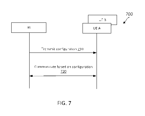
[0072] FIG. 7 is a signaling diagram of a network-specific waveform selection
method 700
according to embodiments of the present disclosure. The method 700 is
implemented among
a BS, a UE A, and a UE B. The BS may be similar to the BSs 105 and 300. The
UEs A and
B may be similar to the UEs 115 and 200. Steps of the method 700 can be
executed by
computing devices (e.g., a processor, processing circuit, and/or other
suitable component) of
the BS and the UEs A and B. As illustrated, the method 700 includes a number
of
enumerated steps, but embodiments of the method 700 may include additional
steps before,
after, and in between the enumerated steps. In some embodiments, one or more
of the
enumerated steps may be omitted or performed in a different order.
[0073] At step 710, the BS transmits a configuration indicating waveform
structures for
various frequency bands (e.g., the frequency bands 610 and 620). For example,
the
configuration may indicate an interlaced frequency structure (e.g., an
interlace 4081(k) or
5081(k)) for a frequency band with a PSD limit and may indicate a non-
interlaced frequency
structure (e.g., including contiguous frequencies) for a frequency band
without a PSD limit.
In an embodiment, the BS may broadcast the configuration in a SIB to all UEs
(e.g., including
the UEs A and B) in a network (e.g., the network 100).
18
CA 03067149 2019-12-11
WO 2019/018112
PCT/US2018/039992
[0074] At step 720, the BS may communicate with the UE A and the UE B
according to the
configuration. The UE A or the UE B may determine whether to use an interlaced
frequency
structure or a non-interlaced frequency structure for communicating with the
BS based on the
waveform structures indicated in the received configuration. When the waveform
structure
for a frequency band indicates an interlaced frequency structure, the BS and
the UE may
communicate with each other using similar mechanisms as in the scheme 400 or
500.
[0075] FIG. 8 is a signaling diagram of a UE-specific waveform selection
method 800
according to embodiments of the present disclosure. The method 800 is
implemented among
a BS, a UE A, and a UE B. The BS may be similar to the BSs 105 and 300. The
UEs A and
B may be similar to the UEs 115 and 200. Steps of the method 800 can be
executed by
computing devices (e.g., a processor, processing circuit, and/or other
suitable component) of
the BS and the UEs A and B. As illustrated, the method 800 includes a number
of
enumerated steps, but embodiments of the method 800 may include additional
steps before,
after, and in between the enumerated steps. In some embodiments, one or more
of the
enumerated steps may be omitted or performed in a different order.
[0076] The method 800 may configure or assign transmissions per UE with an
interlaced
frequency structure or a non-interlaced frequency structure based on power
headroom reports
received from the UEs. For example, when a UE is power-limited, the BS may
schedule a
transmission (e.g., a PUSCH transmission) for the UE with an interlaced
frequency structure.
A UE is power-limited when the required transmit power for a UL transmission
in a particular
communication channel or link exceeds an available transmit power of the UE.
Alternatively,
when a UE is not power-limited, the BS may schedule a transmission for the UE
with a non-
interlaced frequency structure.
[0077] At step 810, the BS transmits a configuration A indicating a waveform
structure for
the UE A. For example, the UE A is power-limited, and thus the waveform
structure may
indicate an interlaced frequency structure (e.g., an interlace 4081(k) or
508)(k)).
[0078] At step 820, the BS transmits a configuration B indicating a waveform
structure for
the UE B. For example, the UE B is not power-limited, and thus the waveform
structure may
indicate a non-interlaced frequency structure (e.g., including contiguous
frequencies).
[0079] At step 830, the BS may communicate with the UE A based on the
configuration A,
for example, using the interlaced frequency structure.
[0080] At step 840, the BS may communicate with the UE B based on the
configuration B,
for example, using the non-interlaced frequency structure.
19
CA 03067149 2019-12-11
WO 2019/018112
PCT/US2018/039992
[0081] In an embodiment, the BS may select an interlaced frequency structure
or a non-
interlaced frequency structure for a UE based on a power headroom of the UE
and a PSD
parameter (e.g., a PSD limit or a range of allowable PSD levels) of a
frequency band. For
example, the BS may schedule the UE A with an interlaced frequency structure
in one
frequency band and a non-interlaced frequency structure in another frequency
band.
Alternatively, the BS may schedule the UE A with an interlaced frequency
structure in one
time period and a non-interlaced frequency structure in another time period.
[0082] FIGS. 9 and 10 illustrate various mechanisms for configuring random
access resources
with an interlaced frequency structure and a non-interlaced frequency
structure.
[0083] FIG. 9 illustrates a random access transmission scheme 900 according to
embodiments
of the present disclosure. The x-axis represents frequency in some constant
units. The
scheme 900 may be employed by BSs such as the BSs 105 and 300 and UEs such as
the UEs
115 and 200. In the scheme 900, a BS may configure multiple sets of random
access
resources in different frequency bands. For example, one set of random access
resources 910
may be located in a frequency band 902 and may have an interlaced frequency
structure (e.g.,
an interlace 4081(k) or 508)(k)). Another set of random access resources 920
may be located in
a frequency band 904 and may have a non-interlaced frequency structure (e.g.,
including
contiguous frequencies). A UE may autonomously select resources from the
resources 910 in
the frequency band 902 or from the resources 920 in the frequency band 904 for
transmitting
a random access signal. The BS may monitor for a random access signal in the
resources 910
based on the interlaced frequency structure and in the resources 920 based on
the non-
interlaced frequency structure.
[0084] In an embodiment, the selection may be based on a DL path loss
measurement. When
a UE is power-limited, the UE may select resources from the resources 910 with
the
interlaced frequency structure for better power utilization. For example, the
UE may transmit
a random access preamble in a frequency interlaced channel similar to the
interlaces 408 and
508. Conversely, when a UE is not power-limited, the UE may select resources
from the
resources 920 with the non-interlaced frequency structure. For example, the UE
may transmit
a random access preamble in contiguous frequencies.
[0085] In an embodiment, a UE may perform power ramping during a random access
procedure. For example, at the beginning of a random access procedure, the UE
may select a
resource from the resources 920 with the non-interlaced frequency structure
for a random
access preamble transmission. When no random access response is received, the
UE may
CA 03067149 2019-12-11
WO 2019/018112
PCT/US2018/039992
increase the transmit power for a subsequent random access transmission. When
the transmit
power reaches a maximum PSD level allowable in the frequency band 904, the UE
may
switch to select a resource from the resources 910 with the interlaced
frequency structure for
a subsequent random access preamble transmission.
[0086] FIG. 10 illustrates a random access transmission scheme 1000 according
to
embodiments of the present disclosure. The x-axis represents time in some
constant units.
The y-axis represents frequency in some constant units. The scheme 1000 may be
employed
by BSs such as the BSs 105 and 300 and UEs such as the UEs 115 and 200. The
scheme
1000 may be substantially similar to the scheme 900. However, a BS may
configure multiple
sets of random access resources in different time periods instead of different
frequency bands
as in the scheme 900. For example, one set of random access resources 1010 may
be located
in a time period 1002 and may have an interlaced frequency structure (e.g., an
interlace 4081(k)
or 508)(k)). Another set of random access resources 1020 may be located in a
time period
1004 and may have a non-interlaced frequency structure (e.g., including
contiguous
frequencies). In an embodiment, resources 1010 and 1020 are located in the
same frequency
band 1001.
[0087] Similar to the scheme 900, a UE may autonomously select resources from
the
resources 1010 in the time period 1002 or from the resources 1020 in the time
period 1004 for
transmitting a random access signal. The selection may be based on a DL path
loss
measurement, a power utilization factor (e.g., a power headroom) of the UE,
and/or a transmit
power used for the random access preamble transmission as described in the
scheme 900.
The BS may monitor for a random access signal in the resources 1010 based on
the interlaced
frequency structure and in the resources 1020 based on the non-interlaced
frequency
structure.
[0088] FIG. 11 illustrates a frequency interlacing scheme 1100 with a reduced
SCS according
to embodiments of the present disclosure. The scheme 1100 may be employed by
BSs such
as the BSs 105 and 300 and UEs such as the UEs 115 and 200 to communicate over
a
frequency spectrum 402. The scheme 1100 may be substantially similar to the
schemes 400
and 500, but may allocate resources at a reduced SCS.
[0089] The frequency spectrum 402 may have a bandwidth of about 20 MHz and a
SCS of
about 60 kHz. Thus, the frequency spectrum 402 includes twenty-five RBs 510
(e.g., indexed
from 0 to 24). As described above with respect to FIG. 5, when allocating
resources in units
of interlaces 508 at an RB-granularity level, the scheme 500 may provide a
power boost of
21
CA 03067149 2019-12-11
WO 2019/018112
PCT/US2018/039992
about 7 dB without the TTI bundling. Instead of further improving power
utilization using
TTI bundling, the scheme 1100 applies frequency interlacing at a reduced SCS.
[0090] The scheme 1100 divides each subcarrier 512 into about four subcarriers
1112. Thus,
each subcarrier 1112 spans about 15 kHz. For example, the subcarrier 512
indexed 0 is
divided into four subcarriers 1112 indexed 0 to 3, the subcarrier 512 indexed
1 is divided into
four subcarriers 1112 indexed 4 to 7, and the subcarrier 512 indexed 2 is
divided into four
subcarriers 1112 indexed 8 to 11. The group of 12 subcarriers 1112 forms a RB
1110.
[0091] Similar to the schemes 400 and 500, the scheme 1100 may allocate
resources in units
of interlaces similar to the interlaces 408 and 508. For example, each
interlace may include
about ten islands 1106 evenly spaced over the spectrum 402, where each island
1106 includes
one RB 1110. Thus, the frequency spectrum may include about ten interlaces.
The
distribution of an allocation's frequency occupancy into ten islands 1106 can
provide a power
boost of about 10 dB. Alternatively, the scheme 1100 may divide each
subcarrier 512 into
about two subcarriers, each spanning about 30 kHz. The reduced SCS can
distribute an
allocation in a frequency domain to allow a transmitter to transmit at a
higher power while
maintaining a certain PSD level.
[0092] In an embodiment, the reduced SCS can increase computational
complexity. For
example, under normal operation with a bandwidth of 20 MHz and a SCS of about
60 kHz, a
512-point Fast Fourier transform (FFT) may be applied. However, reducing the
SCS to about
15 kHz, a 2048-point FFT may be required. The larger FFT-size may increase the
computational complexity. One approach to reducing the computational
complexity is to
segment the 20 MHz bandwidth into about four segments and apply four 512-point
FFTs, one
for each segment.
[0093] In an embodiment, communications in a frequency spectrum below about 6
GHz may
use an interlaced frequency waveform structure and communications in a
frequency spectrum
above about 6 GHz may use an interlaced frequency waveform structure and a non-
interlaced
frequency waveform structure. For example, the schemes 400, 500, and 1100
described with
respect to 4, 5, and 11, respectively, may be used for the interlaced
frequency-based
communications. The schemes 600, 900, and 1000 and the methods 700 and 800
described
with respect to FIGS. 6, 9, 10, 7, and 8, respectively, may be used to select
between the
interlaced frequency waveform structure and the non-interlaced frequency
waveform structure
for communications above 6 GHz.
22
CA 03067149 2019-12-11
WO 2019/018112
PCT/US2018/039992
[0094] FIG. 12 is a flow diagram of a communication method 1200 with a
waveform
selection according to embodiments of the present disclosure. Steps of the
method 1200 can
be executed by a computing device (e.g., a processor, processing circuit,
and/or other suitable
component) of a wireless communication device, such as the BSs 105 and 300 and
the UEs
115 and 200. The method 1200 may employ similar mechanisms as in the schemes
400, 500,
600, 900, and 1000 and the methods 700 and 800 described with respect to FIGS.
4, 5, 6, 9,
10, 7, and 8, respectively. As illustrated, the method 1200 includes a number
of enumerated
steps, but embodiments of the method 1200 may include additional steps before,
after, and in
between the enumerated steps. In some embodiments, one or more of the
enumerated steps
may be omitted or performed in a different order.
[0095] At step 1210, the method 1200 includes selecting, by a first wireless
communication
device, a waveform structure between an interlaced frequency structure and a
non-interlaced
frequency structure for communicating in a frequency spectrum (e.g., the
frequency spectrum
402). The interlaced frequency structure may include at least a first set of
frequency bands
(e.g., the interlace 4081(0) or 5081(0)) in the spectrum. The first set of
frequency bands
interlaces with a second set of frequency bands (e.g., the interlace 4081(1)
or 5081(1)) in the
frequency spectrum. The non-interlaced frequency structure may include one or
more
contiguous frequency bands, RBs, or in the frequency spectrum. The selection
may be band-
dependent as described in the scheme 600, network-specific as described in the
method 700,
or UE-specific as described in the method 800.
[0096] At step 1220, the method 1200 includes communicating, by the first
wireless
communication device with a second wireless communication device, a
communication
signal in the frequency spectrum based on the selected waveform structure.
[0097] Information and signals may be represented using any of a variety of
different
technologies and techniques. For example, data, instructions, commands,
information, signals,
bits, symbols, and chips that may be referenced throughout the above
description may be
represented by voltages, currents, electromagnetic waves, magnetic fields or
particles, optical
fields or particles, or any combination thereof.
[0098] The various illustrative blocks and modules described in connection
with the
disclosure herein may be implemented or performed with a general-purpose
processor, a DSP,
an ASIC, an FPGA or other programmable logic device, discrete gate or
transistor logic,
discrete hardware components, or any combination thereof designed to perform
the functions
described herein. A general-purpose processor may be a microprocessor, but in
the
23
CA 03067149 2019-12-11
WO 2019/018112
PCT/US2018/039992
alternative, the processor may be any conventional processor, controller,
microcontroller, or
state machine. A processor may also be implemented as a combination of
computing devices
(e. g. , a combination of a DSP and a microprocessor, multiple
microprocessors, one or more
microprocessors in conjunction with a DSP core, or any other such
configuration).
[0099] The functions described herein may be implemented in hardware, software
executed
by a processor, firmware, or any combination thereof. If implemented in
software executed by
a processor, the functions may be stored on or transmitted over as one or more
instructions or
code on a computer-readable medium. Other examples and implementations are
within the
scope of the disclosure and appended claims. For example, due to the nature of
software,
functions described above can be implemented using software executed by a
processor,
hardware, firmware, hardwiring, or combinations of any of these. Features
implementing
functions may also be physically located at various positions, including being
distributed such
that portions of functions are implemented at different physical locations.
Also, as used
herein, including in the claims, "or" as used in a list of items (for example,
a list of items
prefaced by a phrase such as "at least one of' or "one or more of') indicates
an inclusive list
such that, for example, a list of [at least one of A, B, or C] means A or B or
C or AB or AC or
BC or ABC (i.e., A and B and C).
[0100] Further embodiments of the present disclosure include a method of
wireless
communication comprising selecting, by a first wireless communication device,
a waveform
structure between an interlaced frequency structure and a non-interlaced
frequency structure
for communicating in a frequency spectrum; and communicating, by the first
wireless
communication device with a second wireless communication device in the
frequency
spectrum, a communication signal based on the selected waveform structure.
[0101] In some embodiments, wherein the interlaced frequency structure
includes at least a
first set of frequency bands in the frequency spectrum, the first set of
frequency bands
interlacing with a second set of frequency bands in the frequency spectrum,
and wherein the
non-interlaced frequency structure includes one or more contiguous frequency
bands in the
frequency spectrum. In some embodiments, wherein the selecting is based on a
power
spectral density (PSD) parameter of the frequency spectrum. In some
embodiments, wherein
the PSD parameter is associated with a PSD requirement in the frequency
spectrum, and
wherein the selecting includes determining whether the frequency spectrum has
the PSD
requirement; and selecting the interlaced frequency structure as the waveform
structure when
determining that the frequency spectrum has the PSD requirement. In some
embodiments,
24
CA 03067149 2019-12-11
WO 2019/018112
PCT/US2018/039992
wherein the PSD parameter is associated with a PSD requirement in the
frequency spectrum,
wherein the selecting is based on a first frequency band having the PSD
requirement and a
second frequency band not having the PSD requirement, and wherein the
communicating
includes communicating a first communication signal with the interlaced
frequency structure
in the first frequency band; and communicating a second communication signal
with the non-
interlaced frequency structure in the second frequency band. In some
embodiments, the
method further comprises transmitting, by the first wireless communication
device, a
configuration indicating the waveform structure for communicating in the
frequency
spectrum. In some embodiments, wherein the selecting is based on a power
headroom of the
second wireless communication device. In some embodiments, the method further
comprises
receiving, by the first wireless communication device from the second wireless
communication device, a configuration indicating the waveform structure for
communicating
in the frequency spectrum, wherein the selecting is based on the
configuration. In some
embodiments, the method further comprises communicating, by the first wireless
communication device with the second wireless communication device, a
configuration
indicating a first set of random access resources having a interlaced
frequency structure and a
second set of random access resources having a non-interlaced frequency
structure; and
communicating, by the first wireless communication device with the second
wireless
communication device, a random access signal based on the configuration. In
some
embodiments, wherein the first set of random access resources and the second
set of random
access resources are in different frequency bands within the frequency
spectrum. In some
embodiments, wherein the first set of random access resources and the second
set of random
access resources are in different time periods. In some embodiments, wherein
the
communicating the configuration includes transmitting, by the first wireless
communication
device to the second wireless communication device, the configuration, and
wherein the
communicating the random access signal includes monitoring, by the first
wireless
communication device, for the random access signal. In some embodiments,
wherein the
communicating the configuration includes receiving, by the first wireless
communication
device from the second wireless communication device, the configuration. In
some
embodiments, the method further comprises determining, by the first wireless
communication
device, whether to transmit the random access signal to the second wireless
communication
device using the first set of random access resources or the second set of
random access
resources based on at least one of the configuration, a power headroom of the
second wireless
CA 03067149 2019-12-11
WO 2019/018112
PCT/US2018/039992
communication device, or a power utilization factor of the second wireless
communication
device. In some embodiments, wherein the communicating the random access
signal includes
transmitting, by the first wireless communication device to the second
wireless
communication device using the second set of random access resources, a first
random access
signal with the non-interlaced frequency structure at a first transmit power;
and transmitting,
by the first wireless communication device to the second wireless
communication device
using the first set of random access resources, a second random access signal
with the
interlaced frequency structure at a second transmit power greater than the
first transmit
power. In some embodiments, the method further comprises determining, by the
first
wireless communication device, to transmit the second random access signal
with the
interlaced frequency structure using the first set of random access resources
based on a
comparison between the second transmit power and a power spectral density
(PSD) parameter
of a frequency band of the second set of random access resources. In some
embodiments,
wherein the frequency spectrum includes a first subcarrier spacing for the non-
interlaced
frequency structure, wherein the communicating the communication signal
includes
communicating the communication signal using a second subcarrier spacing for
the interlaced
frequency structure, and wherein the first subcarrier spacing is greater than
the second
subcarrier spacing.
[0102] Further embodiments of the present disclosure include an apparatus
comprising a
processor configured to select a waveform structure between an interlaced
frequency structure
and a non-interlaced frequency structure for communicating in a frequency
spectrum; and a
transceiver configured to communicate, with a second wireless communication
device in the
frequency spectrum, a communication signal based on the selected waveform
structure.
[0103] In some embodiments, wherein the interlaced frequency structure
includes at least a
first set of frequency bands in the frequency spectrum, the first set of
frequency bands
interlacing with a second set of frequency bands in the frequency spectrum,
and wherein the
non-interlaced frequency structure includes one or more contiguous frequency
bands in the
frequency spectrum. In some embodiments, wherein the processor is further
configured to
select the waveform structure based on a power spectral density (PSD)
parameter of the
frequency spectrum. In some embodiments, wherein the PSD parameter is
associated with a
PSD requirement in the frequency spectrum, and wherein the processor is
further configured
to select the waveform structure by determining whether the frequency spectrum
has a PSD
requirement; and selecting the interlaced frequency structure as the waveform
structure when
26
CA 03067149 2019-12-11
WO 2019/018112
PCT/US2018/039992
determining that the frequency spectrum has the PSD requirement. In some
embodiments,
wherein the PSD parameter is associated with a PSD requirement in the
frequency spectrum,
wherein the processor is further configured to select the waveform structure
based on a first
frequency band having the PSD requirement and a second frequency band not
having the PSD
requirement, and wherein the transceiver is further configured to communicate
a first
communication signal with the interlaced frequency structure in the first
frequency band; and
communicate a second communication signal with the non-interlaced frequency
structure in
the second frequency band. In some embodiments, wherein the transceiver is
further
configured to transmit a configuration indicating the waveform structure for
communicating
in the frequency spectrum. In some embodiments, wherein the processor is
further
configured to select the waveform structure based on a power headroom of the
second
wireless communication device. In some embodiments, wherein the transceiver is
further
configured to receive, from the second wireless communication device, a
configuration
indicating the waveform structure for communicating in the frequency spectrum,
and wherein
the processor is further configured to select the waveform structure based on
the
configuration. In some embodiments, wherein the transceiver is further
configured to
communicate, with the second wireless communication device, a configuration
indicating a
first set of random access resources having an interlaced frequency structure
and a second set
of random access resources having a non-interlaced frequency structure; and
communicate,
with the second wireless communication device, a random access signal based on
the
configuration. In some embodiments, wherein the first set of random access
resources and
the second set of random access resources are in different frequency bands
within the
frequency spectrum. In some embodiments, wherein the first set of random
access resources
and the second set of random access resources are in different time periods.
In some
embodiments, wherein the transceiver is further configured to communicate the
configuration
by transmitting, to the second wireless communication device, the
configuration; and
communicate the random access signal by monitoring for the random access
signal. In some
embodiments, wherein the transceiver is further configured to communicate the
configuration
by receiving, from the second wireless communication device, the
configuration. In some
embodiments, wherein the processor is further configured to determine whether
to transmit
the random access signal to the second wireless communication device using the
first set of
random access resources or the second set of random access resources based on
at least one of
the configuration, a power headroom of the second wireless communication
device, or a
27
CA 03067149 2019-12-11
WO 2019/018112
PCT/US2018/039992
power utilization factor of the second wireless communication device. In some
embodiments,
wherein the transceiver is further configured to communicate the random access
signal by
transmitting, to the second wireless communication device using the second set
of random
access resources, a first random access signal with the non-interlaced
frequency structure at a
first transmit power; and transmitting, to the second wireless communication
device using the
first set of random access resources, a second random access signal with the
interlaced
frequency structure at a second transmit power greater than the first transmit
power. In some
embodiments, wherein the processor is further configured to determine to
transmit the second
random access signal with the interlaced frequency structure using the first
set of random
access resources based on a comparison between the second transmit power and a
power
spectral density (PSD) parameter of a frequency band of the second set of
random access
resources. In some embodiments, wherein the frequency spectrum includes a
first SCS for
the non-interlaced frequency structure, wherein the transceiver is further
configured to
communicate the communication signal by communicating the communication signal
using a
second SCS for the interlaced frequency structure, and wherein the first SCS
is greater than
the second SCS.
[0104] Further embodiments of the present disclosure include a computer-
readable medium
having program code recorded thereon, the program code comprising code for
causing a first
wireless communication device to select a waveform structure between an
interlaced
frequency structure and a non-interlaced frequency structure for communicating
in a
frequency spectrum; and code for causing the first wireless communication
device to
communicate, with a second wireless communication device in the frequency
spectrum, a
communication signal based on the selected waveform structure.
[0105] In some embodiments, wherein the interlaced frequency structure
includes at least a
first set of frequency bands in the frequency spectrum, the first set of
frequency bands
interlacing with a second set of frequency bands in the frequency spectrum,
and wherein the
non-interlaced frequency structure includes one or more contiguous frequency
bands in the
frequency spectrum. In some embodiments, wherein the code for causing the
first wireless
communication device to select the waveform structure is further configured to
select the
waveform structure based on a power spectral density (PSD) parameter of the
frequency
spectrum. In some embodiments, wherein the PSD parameter is associated with a
PSD
requirement in the frequency spectrum, and wherein the code for causing the
first wireless
communication device to select the waveform structure is further configured to
select the
28
CA 03067149 2019-12-11
WO 2019/018112
PCT/US2018/039992
waveform structure by determining whether the frequency spectrum has the PSD
requirement; and selecting the interlaced frequency structure as the waveform
structure when
determining that the frequency spectrum has the PSD requirement. In some
embodiments,
wherein the PSD parameter is associated with a PSD requirement in the
frequency spectrum,
wherein the code for causing the first wireless communication device to select
the waveform
structure is further configured to select the waveform structure based on a
first frequency
band having the PSD requirement and a second frequency band not having the PSD
requirement, and wherein the code for causing the first wireless communication
device to
communicate the communication signal is further configured to communicate the
communicate signal by communicating a first communication signal with the
interlaced
frequency structure in the first frequency band; and communicating a second
communication
signal with the non-interlaced frequency structure in the second frequency
band. In some
embodiments, the computer-readable medium further comprises code for causing
the first
wireless communication device to transmit a configuration indicating the
waveform structure
for communicating in the frequency spectrum. In some embodiments, wherein the
code for
causing the first wireless communication device to select the waveform
structure is further
configured to select the waveform structure based on a power headroom of the
second
wireless communication device. In some embodiments, the computer-readable
medium
further comprises code for causing the first wireless communication device to
receive, from
the second wireless communication device, a configuration indicating the
waveform structure
for communicating in the frequency spectrum, wherein the code for causing the
first wireless
communication device to select the waveform structure is further configured to
select the
waveform structure based on the configuration. In some embodiments, the
computer-
readable medium further comprises code for causing the first wireless
communication device
to communicate, with the second wireless communication device, a configuration
indicating a
first set of random access resources having an interlaced frequency structure
and a second set
of random access resources having a non-interlaced frequency structure; and
code for causing
the first wireless communication device to communicate, with the second
wireless
communication device, a random access signal based on the configuration. In
some
embodiments, wherein the first set of random access resources and the second
set of random
access resources are in different frequency bands within the frequency
spectrum. In some
embodiments, wherein the first set of random access resources and the second
set of random
access resources are in different time periods. In some embodiments, wherein
the code for
29
CA 03067149 2019-12-11
WO 2019/018112
PCT/US2018/039992
causing the first wireless communication device to communicate the
configuration is further
configured to transmit, to the second wireless communication device, the
configuration, and
wherein the code for causing the first wireless communication device to
communicate the
random access signal is further configured to monitor for the random access
signal. In some
embodiments, wherein the code for causing the first wireless communication
device to
communicate the configuration is further configured to receive, from the
second wireless
communication device, the configuration. In some embodiments, the computer-
readable
medium further comprises code for causing the first wireless communication
device to
determine whether to transmit the random access signal to the second wireless
communication device using the first set of random access resources or the
second set of
random access resources based on at least one of the configuration, a power
headroom of the
second wireless communication device, or a power utilization factor of the
second wireless
communication device. In some embodiments, wherein the code for causing the
first wireless
communication device to communicate the random access signal is further
configured to
transmit, to the second wireless communication device using the second set of
random access
resources, a first random access signal with the non-interlaced frequency
structure at a first
transmit power; and transmit, to the second wireless communication device
using the first set
of random access resources, a second random access signal with the interlaced
frequency
structure at a second transmit power greater than the first transmit power. In
some
embodiments, the computer-readable medium further comprises code for causing
the first
wireless communication device to determine to transmit the second random
access signal with
the interlaced frequency structure using the first set of random access
resources based on a
comparison between the second transmit power and a power spectral density
(PSD) parameter
of a frequency band of the second set of random access resources. In some
embodiments,
wherein the frequency spectrum includes a first SCS for the non-interlaced
frequency
structure, wherein the code for causing the first wireless communication
device to
communicate the communication signal is further configured to communicate the
communication signal using a second SCS for the interlaced frequency
structure, and wherein
the first SCS is greater than the second SCS.
[0106] Further embodiments of the present disclosure include an apparatus
comprising means
for selecting a waveform structure between an interlaced frequency structure
and a non-
interlaced frequency structure for communicating in a frequency spectrum; and
means for
CA 03067149 2019-12-11
WO 2019/018112
PCT/US2018/039992
communicating, with a second wireless communication device in the frequency
spectrum, a
communication signal based on the selected waveform structure.
[0107] In some embodiments, wherein the interlaced frequency structure
includes at least a
first set of frequency bands in the frequency spectrum, the first set of
frequency bands
interlacing with a second set of frequency bands in the frequency spectrum,
and wherein the
non-interlaced frequency structure includes one or more contiguous frequency
bands in the
frequency spectrum. In some embodiments, wherein the means for selecting the
waveform
structure is further configured to select the waveform structure based on a
power spectral
density (PSD) parameter of the frequency spectrum. In some embodiments,
wherein the PSD
parameter is associated with a PSD requirement in the frequency spectrum, and
wherein the
means for selecting the waveform structure is further configured to select the
waveform
structure by determining whether the frequency spectrum has the PSD
requirement; and
selecting the interlaced frequency structure as the waveform structure when
determining that
the frequency spectrum has the PSD requirement. In some embodiments, wherein
the PSD
parameter is associated with a PSD requirement in the frequency spectrum,
wherein the
means for selecting the waveform structure is further configured to select the
waveform
structure based on a first frequency band having the PSD requirement and a
second frequency
band not having the PSD requirement, and wherein the means for communicating
the
communication signal is further configured to communicate a first
communication signal with
the interlaced frequency structure in the first frequency band; and
communicate a second
communication signal with the non-interlaced frequency structure in the second
frequency
band. In some embodiments, the apparatus further comprises means for
transmitting a
configuration indicating the waveform structure for communicating in the
frequency
spectrum. In some embodiments, wherein the means for selecting the waveform
structure is
further configured to select the waveform structure based on a power headroom
of the second
wireless communication device. In some embodiments, the apparatus further
comprises
means for receiving, from the second wireless communication device, a
configuration
indicating the waveform structure for communicating in the frequency spectrum,
wherein the
means for selecting the waveform structure is further configured to select the
waveform
structure based on the configuration. In some embodiments, the apparatus
further comprises
means for communicating, with the second wireless communication device, a
configuration
indicating a first set of random access resources having an interlaced
frequency structure and
a second set of random access resources having a non-interlaced frequency
structure; and
31
CA 03067149 2019-12-11
WO 2019/018112
PCT/US2018/039992
means for communicating, with the second wireless communication device, a
random access
signal based on the configuration. In some embodiments, wherein the first set
of random
access resources and the second set of random access resources are in
different frequency
bands within the frequency spectrum. In some embodiments, wherein the first
set of random
access resources and the second set of random access resources are in
different time periods.
In some embodiments, wherein the means for communicating the configuration is
further
configured to transmit, to the second wireless communication device, the
configuration, and
wherein the means for communicating the random access signal is further
configured to
monitor for the random access signal. In some embodiments, wherein the means
for
communicating the configuration is further configured to receive, from the
second wireless
communication device, the configuration. In some embodiments, the apparatus
further
comprises means for determining whether to transmit the random access signal
to the second
wireless communication device using the first set of random access resources
or the second
set of random access resources based on at least one of the configuration, a
power headroom
of the second wireless communication device, or a power utilization factor of
the second
wireless communication device. In some embodiments, wherein the means for
communicating the random access signal is further configured to transmit, to
the second
wireless communication device using the second set of random access resources,
a first
random access signal with the non-interlaced frequency structure at a first
transmit power;
and transmit, to the second wireless communication device using the first set
of random
access resources, a second random access signal with the interlaced frequency
structure at a
second transmit power greater than the first transmit power. In some
embodiments, the
apparatus further comprises means for determining to transmit the second
random access
signal with the interlaced frequency structure using the first set of random
access resources
based on a comparison between the second transmit power and a power spectral
density
(PSD) parameter of a frequency band of the second set of random access
resources. In some
embodiments, wherein the frequency spectrum includes a first SCS for the non-
interlaced
frequency structure, wherein the means for communicating the communication
signal is
further configured to communicate the communication signal using a second SCS
for the
interlaced frequency structure, and wherein the first SCS is greater than the
second SCS.
[0108] As those of some skill in this art will by now appreciate and depending
on the
particular application at hand, many modifications, substitutions and
variations can be made
in and to the materials, apparatus, configurations and methods of use of the
devices of the
32
CA 03067149 2019-12-11
WO 2019/018112
PCT/US2018/039992
present disclosure without departing from the spirit and scope thereof. In
light of this, the
scope of the present disclosure should not be limited to that of the
particular embodiments
illustrated and described herein, as they are merely by way of some examples
thereof, but
rather, should be fully commensurate with that of the claims appended
hereafter and their
functional equivalents.
33