Note: Descriptions are shown in the official language in which they were submitted.
CA 03067183 2019-12-12
BATTERY PACK AND ELECTRIC APPARATUS USING BATTERY PACK
[Technical Field]
[0001]
The present disclosure relates to an electric apparatus such as a motor or
lighting having
a load, and a battery pack supplying power to such an electric apparatus.
[Background Art]
[0002]
Electric apparatuses such as power tools are driven by battery packs using
secondary
batteries such as lithium ion batteries, and therefore cordless electric
apparatuses have been
devised. For example, a battery pack accommodating a plurality of secondary
battery cells is
used in handheld power tools in which a tip tool is driven by a motor, and the
motor is driven by
electric energy stored in the battery pack. The battery pack is configured to
be attachable to
and detachable from a power tool main body. When a voltage drops due to
discharging, the
battery pack is detached from the power tool main body and is charged using an
external
charging device.
[0003]
Cordless power tools and electric apparatuses need to maintain a predetermined
operation time and to maintain a predetermined output, and therefore higher
outputs and higher
voltages have been achieved as performance of secondary batteries has
improved. In addition,
as electric apparatuses using battery packs as a power source have been
developed, battery packs
using various voltages have become commercialized. In general, battery packs
have a fixed
output voltage. However, Patent Literature 1 proposes a power source device
for an electric
apparatus, in which a plurality of battery units are provided inside a housing
accommodating
batteries and which can select an output in series-connection or an output in
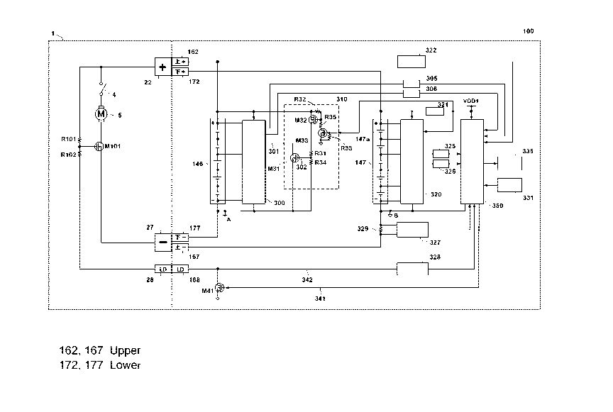
parallel-connection
using a connection means so that the device can support apparatuses using
different voltages.
[Citation List]
[Patent Literature]
[0004]
[Patent Literature 1]
Japanese Patent Laid-Open No. 2014-17954
Summary of Invention
[Technical Problem]
1
CA 03067183 2019-12-12
[0005]
It is troublesome for a user to prepare a plurality of kinds of battery packs
when using a
plurality of electric apparatuses, and therefore it is desired to realize a
convenient battery pack
that supports electric apparatuses using different voltages by switching the
voltage.
Furthermore, instead of a power source device that is separate from an
electric apparatus main
body as in Patent Literature 1, it has been desired to realize voltage
switchable battery packs that
can be easily mounted in electric apparatuses.
[0006]
According to the present disclosure, there are provided a battery pack capable
of
switching an output voltage so that it can be shared between electric
apparatuses using different
voltages, and an electric apparatus using the battery pack.
In addition, according to an aspect of the present disclosure, there is
provided a battery
pack that can be mounted in an electric apparatus main body. The battery pack
can switch a
connection state of a plurality of cell units.
In addition, according to the aspect of the present disclosure, there is
provided a battery
pack including a controller that can control discharging or charging of the
battery pack while
monitoring the state of the plurality of cell units.
In addition, according to the aspect of the present disclosure, there is
provided a battery
pack in which discharging or charging of the battery pack can be stably
controlled regardless of
the connection state of the plurality of cell units.
According to another aspect of the present disclosure, there are provided a
battery pack
that balances consumption currents of a plurality of cell units included in
the battery pack that is
switchable between output voltages such as a high voltage and a low voltage,
and an electric
apparatus using the battery pack.
According to still another aspect of the present disclosure, there is provided
a battery
pack in which a microcomputer is provided in any one of battery cell
protection circuits
provided in a plurality of cell units.
According to still another aspect of the present disclosure, there is provided
a battery
pack that can efficiently draw out capability of an electric apparatus.
According to still another aspect of the present disclosure, there is provided
a
high-function battery pack.
According to still another aspect of the present disclosure, there is provided
a battery
pack having a terminal structure that can be favorably fitted into a
connection terminal on an
electric apparatus main body side.
2
CA 03067183 2019-12-12
[Solution to Problem]
[0007]
The following is description of representative features of the disclosure
disclosed in this
application.
A feature of the battery pack according to a first aspect of the disclosure is
as follows.
There is provided a battery pack including at least first and second cell
units as cell
units in which a plurality of battery cells are connected in series. The cell
units are configured
to be switched between a series-connection state in which the first and second
cell units are
connected to each other in series while the first cell unit is connected to a
higher voltage side
than the second cell unit and a connection state other than the series-
connection state. The
battery pack includes a controller that is directly or indirectly connected to
the first and second
cell units and is configured to monitor a state of the battery cells
constituting the first cell unit
and a state of the battery cells constituting the second cell unit and to be
able to output a control
signal for controlling discharging of the battery pack; a power source circuit
that is connected to
the controller and is configured to be able to supply a power source voltage
to the controller; and
a casing that accommodates the first cell unit, the second cell unit, the
controller, and the power
source circuit and is configured to be able to connect the battery pack to an
electric apparatus
main body. The power source circuit is configured to be connected to one cell
unit of the first
and second cell units, the controller is configured to be connected to the
power source circuit and
a negative electrode of the one cell unit, and the power source circuit is
configured to generate
the power source voltage from a voltage input from the one cell unit and to
supply the power
source voltage to the controller.
According to the first aspect of the disclosure, it is possible to provide a
battery pack
that can be mounted in an electric apparatus main body. The battery pack can
switch a
connection state of a plurality of cell units. In addition, it is possible to
provide a battery pack
including the controller that can control discharging of the battery pack
while monitoring the
state of the plurality of cell units. Moreover, it is possible to provide a
battery pack in which
discharging of the battery pack can be stably controlled regardless of the
connection state of the
plurality of cell units because a circuit for supplying a power source voltage
to the controller is
closed in one cell unit.
[0008]
A feature of the battery pack according to a second aspect of the disclosure
is as
follows.
The battery pack includes a first protection circuit that is connected to the
first cell unit
3
CA 03067183 2019-12-12
and monitors a state of the battery cells constituting the first cell unit and
a second protection
circuit that is connected to the second cell unit and monitors a state of the
battery cells
constituting the second cell unit. The controller is configured to be
connected to the first and
second protection circuits and is configured to be able to monitor the state
of the battery cells
constituting the first cell unit via the first protection circuit and to
monitor the state of the battery
cells constituting the second cell unit via the second protection circuit.
[0009]
A feature of the battery pack according to a third aspect of the disclosure is
as follows.
In the battery pack, the power source circuit is configured to be connected to
the second
cell unit as the one cell unit such that the power source voltage is supplied
from the second cell
unit to the controller via the power source circuit.
[0010]
A feature of the battery pack according to a fourth aspect of the disclosure
is as follows.
The battery pack has a signal terminal that is configured to be able to be
connected to
the electric apparatus main body, and the control signal output from the
controller is configured
to be output to the electric apparatus main body via the signal terminal.
[0011]
A feature of the battery pack according to a fifth aspect of the disclosure is
as follows.
In the battery pack, a consumption current controller is connected to the
other cell unit
of the first and second cell units, and the consumption current controller is
configured to
consume power having substantially the same magnitude as power consumed by the
controller.
[0012]
A feature of the battery pack according to a sixth aspect of the disclosure is
as follows.
In the battery pack, the consumption current controller is configured to also
consume
power when the controller consumes power.
[0013]
A feature of the battery pack according to a seventh aspect of the disclosure
is as
follows.
The battery pack has a detection unit that is connected to the controller, and
the
detection unit is configured to detect a physical quantity related to the
battery pack or the electric
apparatus main body connected to the battery pack and to be able to output
information of the
physical quantity to the controller.
[0014]
A feature of the battery pack according to an eighth aspect of the disclosure
is as
4
CA 03067183 2019-12-12
follows.
The battery pack has a first voltage detection unit as the detection unit
connecting the
other cell unit of the first and second cell units and the controller to each
other, and the first
voltage detection unit is configured to output information of a voltage of the
first cell unit to the
controller as the physical quantity.
[0015]
A feature of the battery pack according to a ninth aspect of the disclosure is
as follows.
In the battery pack, the controller is configured to control discharging or
charging of the
battery pack depending on whether the battery pack is in the series-connection
state or a
connection state other than the series-connection state.
[0016]
A feature of the battery pack according to a tenth aspect of the disclosure is
as follows.
The battery pack has a current detection unit as the detection unit for
detecting a current
flowing in at least one battery cell of the plurality of battery cells
constituting the first and
second cell units, and the current detection unit is configured to output
information of a current
flowing in the battery cell to the controller as the physical quantity.
[0017]
A feature of the battery pack according to an eleventh aspect of the
disclosure is as
follows.
The battery pack has a temperature detection unit as the detection unit for
detecting a
temperature of at least one battery cell of the plurality of battery cells
constituting the first and
second cell units, and the temperature detection unit is configured to output
information of the
temperature of the battery cell to the controller as the physical quantity.
[0018]
A feature of the battery pack according to a twelfth aspect of the disclosure
is as
follows.
The battery pack has a second voltage detection unit as the detection unit
configured to
be able to be connected to a terminal of the electric apparatus main body, and
the second voltage
detection unit is configured to output information of a voltage input from the
terminal of the
electric apparatus main body to the controller as the physical quantity.
[0019]
A feature of the battery pack according to a thirteenth aspect of the
disclosure is as
follows.
In the battery pack, the controller is configured to change a condition for
overload
5
CA 03067183 2019-12-12
protection in accordance with a kind of the electric apparatus main body.
[0020]
A feature of the battery pack according to a fourteenth aspect of the
disclosure is as
follows.
There is provided an electric apparatus including the battery pack, and at
least a first
electric apparatus main body as an electric apparatus main body that is able
to be connected to
the battery pack. When the battery pack is connected to the first electric
apparatus main body,
the battery pack is in a series-connection state in which the first and second
cell units are
connected to each other in series.
A second electric apparatus main body has a
.. parallel-connection circuit connecting the first and second cell units to
each other in parallel.
When the battery pack is connected to the second electric apparatus main body,
the battery pack
is in a parallel-connection state, and when the battery pack is not connected
to the first electric
apparatus main body, the battery pack is in a non-connection state in which
the first and second
cell units are electrically independent from each other.
[0021]
A feature of the battery pack according to a fifteenth aspect of the
disclosure is as
follows.
There is provided the battery pack including a plurality of cell units in
which a plurality
of battery cells are connected in series. The cell units are switchable
between an output of
series-connection and an output of parallel-connection. A protection circuit
that monitors a
state of the battery cells is provided for every cell unit. A microcomputer to
which signals of a
plurality of protection circuits are input such that all the battery packs are
monitored is provided
in the protection circuit that is provided in the cell unit of the plurality
of cell units in a
lowermost stage connected to a ground side at a time of series-connection. In
addition, a power
.. source circuit that generates power for driving the microcomputer is
provided, and the power
source circuit generates the power from an output of the cell unit in the
lowermost stage that
becomes close to the ground side at the time of series-connection. There are
two cell units
constituted of an upper stage cell unit (first cell unit) that is disposed on
a side close to a positive
electrode terminal at the time of series-connection and a lower stage cell
unit (second cell unit)
that is disposed on a side close to a negative electrode terminal. When the
battery pack is
mounted in the electric apparatus main body, a connection form of the upper
stage cell unit and
the lower stage cell unit is set to any one of series-connection and parallel-
connection.
[0022]
According to another feature of the present disclosure, the battery pack has
the signal
6
CA 03067183 2019-12-12
terminal for sending out a stoppage signal (discharging stoppage signal) to
the electric apparatus
main body. When an output of an abnormality is detected from any of the
plurality of
protection circuits, the microcomputer outputs a stoppage signal for stopping
an operation of a
motor of the connected electric apparatus main body. In addition, the
protection circuit
connected to the upper stage cell unit is configured to serve as a battery
protection IC (integrated
circuit) which individually monitors voltages between terminals of the battery
cells included in
the upper stage cell unit, and the protection circuit connected to the lower
stage cell unit is
configured to serve as a battery management IC in which a function of a
protection circuit IC
and a microcomputer are integrated in one chip. Here, an adjustment circuit
for balancing total
power consumption of the protection circuit including the microcomputer in the
lower stage cell
unit and power consumption of the protection circuit in the upper stage cell
unit is provided,
such that power consumption of the protection circuits becomes uniform. The
adjustment
circuit has a dummy load for consuming power as much as that consumed by the
microcomputer.
Here, the adjustment circuit is provided in a circuit on the upper stage cell
unit side where the
microcomputer is not provided.
[0023]
According to still another feature of the present disclosure, the
microcomputer has a
sleep function in which power is turned off by itself when not in operation,
and the adjustment
circuit includes a circuit for causing the protection circuit on the upper
stage cell unit side to be
in a sleep state when the microcomputer is in a sleep mode. Moreover, the
protection circuit
has a voltage balance adjusting function of balancing voltages at both ends of
the plurality of
cells. Two sets of positive electrode terminal and negative electrode terminal
are provided
independently in the battery pack. The upper stage cell unit is connected to
the positive
electrode terminal and the negative electrode terminal of one set, and the
lower stage cell unit is
connected to the positive electrode terminal and the negative electrode
terminal of the other set.
When the battery pack is connected to a high-voltage electric apparatus main
body, the upper
stage cell unit and the lower stage cell unit are in the series-connection
state. When the battery
pack is connected to a low-voltage electric apparatus main body, the upper
stage cell unit and the
lower stage cell unit are in the parallel-connection state. When the battery
pack is not mounted
in a different apparatus, power lines of the upper stage cell unit and the
lower stage cell unit are
in a separated state.
[0024]
According to still another feature of the present disclosure, the battery pack
in which an
output voltage is switched by changing two cell units between series-
connection and
7
CA 03067183 2019-12-12
parallel-connection, is provided with the first protection circuit that
monitors the state of the
battery cells in the first cell unit on the high voltage side at the time of
series-connection and the
second protection circuit that monitors the state of the battery cells in the
second cell unit on a
low voltage side at the time of series-connection. A discharging prohibition
signal or a
charging prohibition signal is sent out to the connected electric apparatus
main body side by
monitoring the output states of the first and second protection circuits using
the microcomputer.
Since power for the microcomputer is generated from an output of the second
cell unit by the
power source circuit, power can be stably generated from the cell unit on a
side where a ground
potential does not change even at the time of series-connection or at the time
of
parallel-connection. Various electric apparatuses and power tools can be
operated using the
battery pack described above.
[0025]
According to still another feature of the present disclosure, the battery pack
has the first
cell unit and the second cell unit in which a plurality of cells are connected
in series. An output
of series-connection or an output of parallel-connection of the first cell
unit and the second cell
unit are switchable depending on a connected electric apparatus main body.
The
microcomputer that monitors the first cell unit and the second cell unit is
provided. The
microcomputer determines whether an output of series-connection of the first
cell unit and the
second cell unit is supplied or an output of parallel-connection is supplied
to the connected
electric apparatus main body side and changes a condition for overload
protection in accordance
with a determination result. The condition for overload protection is a limit
value for a current
flowing in the first cell unit or the second cell unit. When the microcomputer
detects that the
current has exceeded the limit value, a stoppage signal for stopping an
operation of the electric
apparatus main body is output.
[0026]
According to still another feature of the present disclosure, two sets of
positive
electrode terminal and negative electrode terminal are provided independently.
The first cell
unit is connected to the positive electrode terminal and the negative
electrode terminal of one set,
and the second cell unit is connected to the positive electrode terminal and
the negative electrode
terminal of the other set. When the battery pack is connected to a high-
voltage electric
apparatus main body, the first cell unit and the second cell unit are in the
series-connection state.
When the battery pack is connected to a low-voltage electric apparatus main
body, the first cell
unit and the second cell unit are in the parallel-connection state. The
protection circuit that
monitors the state of the battery cells is provided for every cell unit. The
microcomputer that
8
CA 03067183 2019-12-12
monitors the plurality of protection circuits is provided in the protection
circuit of any cell unit
of the plurality of cell units. The microcomputer determines whether an output
of the battery
pack is an output in the series-connection state or an output in the parallel-
connection state by
comparing the ground potential of the positive electrode in the first cell
unit provided on a side
close to the positive electrode terminal when the first cell unit and the
second cell unit are in
series-connection and the ground potential of the positive electrode in the
second cell unit. The
limit value (condition for overload protection) for a current is switched
between when the battery
pack is connected to a high-voltage electric apparatus main body and when the
battery pack is
connected to a low-voltage electric apparatus main body. It is favorable that
the limit value for
a current when the battery pack is connected to a high-voltage electric
apparatus main body be
larger than the limit value for a current when the battery pack is connected
to a low-voltage
electric apparatus main body. Only the limit value for a current when the
battery pack is
connected to a low-voltage electric apparatus main body may be set without
setting the limit
value for a current when the battery pack is connected to a high-voltage
electric apparatus main
body.
[0027]
According to still another feature of the present disclosure, the battery pack
has an LD
terminal (abnormality signal terminal) for outputting a discharging stoppage
signal output from
the microcomputer. A semiconductor switching element is provided between the
LD terminal
and the ground. When a discharging stoppage signal is emitted from the
microcomputer, the
LD terminal is subjected to grounding by inputting the discharging stoppage
signal of the
microcomputer to a gate signal of the semiconductor switching element. When
the battery
pack is not mounted in a different apparatus, the power lines of the first
cell unit and the second
cell unit are in an electrically separated state. In addition, the condition
for overload protection
includes any one of or both an allowable upper limit temperature of the first
cell unit and the
second cell unit and an upper limit voltage value at the time of charging.
When the
microcomputer detects that the value has exceeded the upper limit value, a
discharging stoppage
signal for stopping an operation of the electric apparatus main body is
output.
[0028]
According to still another feature of the present disclosure, the protection
circuit that
monitors the state of the battery cells is provided in each of an upper level
cell unit and a lower
level cell unit. The microcomputer is provided in the protection circuit on
the lower level cell
unit side positioned on the ground side at the time of series-connection. The
microcomputer
determines whether an output in the series-connection state is supplied or an
output in the
9
CA 03067183 2019-12-12
parallel-connection state is supplied to the electric apparatus main body side
by also inputting a
signal of the protection circuit on the upper level cell unit side and
comparing the potential of the
positive electrode in the upper level cell unit and the potential of the
positive electrode in the
lower level cell unit and changes the condition for overload protection in
accordance with a
determination result.
[Advantageous Effects of Invention]
[0029]
According to the present disclosure, it is possible to provide the battery
pack that can be
mounted in the electric apparatus main body. The battery pack can switch the
connection state
.. of the plurality of cell units. In addition, it is possible to provide the
battery pack including the
controller that can control discharging or charging of the battery pack while
monitoring the state
of the plurality of cell units. Moreover, it is possible to provide the
battery pack in which
discharging or charging of the battery pack can be stably controlled
regardless of the connection
state of the plurality of cell units.
In addition, since an appropriate output voltage can be automatically obtained
by only
mounting the battery pack in the electric apparatus main body without
depending on a
mechanical switching mechanism for switching the output voltage, the battery
pack can be
shared between electric apparatuses using different voltages.
In addition, since the protection circuit that monitors the state of the
battery cells is
provided for every cell unit, the balance of a consumption current can be
adjusted for every
battery cell.
Moreover, since the adjustment circuit for balancing the total power
consumption of the
protection circuit including the microcomputer in the lower stage cell unit
and power
consumption of the protection circuit in the upper stage cell unit is provided
on the upper stage
cell unit side, deterioration in voltage balance between the cell units can be
suppressed.
In addition, since the condition for overload protection can be changed in
accordance
with the kind of the electric apparatus main body, it is possible to realize
the battery pack in
which capability of the electric apparatus can be drawn out efficiently.
Brief Description of Drawings
[0030]
Fig. 1 is a view for describing a situation of mounting a battery pack
according to the
present disclosure in a power tool.
Fig. 2 is a perspective view illustrating a shape of a battery pack mounting
portion 10 of
CA 03067183 2019-12-12
a power tool main body 1 in Fig. 1.
Fig. 3 is a perspective view of a battery pack 100 according to an example of
the present
disclosure.
Fig. 4 is a perspective view of a state where an upper casing 110 of the
battery pack 100
in Fig. 3 is detached.
Fig. 5 is a view illustrating a shape of a single body of power terminals (161
and 171,
162 and 172, and 167 and 177) in Fig. 4, (1) is a perspective view of the
entirety, (2) is a
perspective view of an upper terminal component 200, and (3) is a perspective
view of a lower
terminal component 220.
Fig. 6 is a perspective view illustrating a state connecting the power
terminals to the
power tool main body, (1) illustrates a state where the power terminals are
connected to a power
tool main body 30 of the present example, and (2) illustrates a state where
the power terminals
are connected to the power tool main body 1 in the related art.
Fig. 7(1) is a perspective view of a terminal portion 50 of the power tool
main body 30
of the present example, and Fig. 7(2) is a view illustrating a connection
situation of the terminal
portion 50 and the power terminals of the battery pack 100.
Fig. 8(1) is a perspective view of a terminal portion 20 of the power tool
main body 1 in
the related art, and Fig. 8(2) is a view illustrating a connection situation
of the terminal portion
and the power terminals of the battery pack 100.
20
Fig. 9 is a view illustrating a shape of a single body of a signal terminal
component 240
in Fig. 4, (1) is a perspective view viewed from the front on the left side,
and (2) is a perspective
view viewed from below on the right side.
Fig. 10 is a view illustrating a situation of fixing a plurality of signal
terminal
components 240 to a circuit board 150, (1) is a view viewed from the front,
(2) is a view of the
signal terminal component 240 viewed from the left, and (3) is a bottom view
of that in (1)
viewed from a lower side.
Fig. 11 is a view illustrating shapes of a connection terminal group in Fig. 4
and a board
cover 180 disposed around thereof, (1) is a perspective view, (2) is a front
view, and (3) is an
enlarged view of a part of the board cover 180 in (2).
Fig. 12 is a perspective view of the upper casing 110 in Fig. 3.
Fig. 13 is a perspective view for describing a method of applying a resin to
the circuit
board 150.
Fig. 14 is a view illustrating a first modification example of the present
example, (1) is
a perspective view of an upper terminal component 260 and a lower terminal
component 280, (2)
11
CA 03067183 2019-12-12
is a left-side view, and (3) is a front view.
Fig. 15 is a view illustrating a second modification example of the present
example and
is a perspective view illustrating the upper terminal component 260 and a
lower terminal
component 280A.
Fig. 16 is a perspective view illustrating an upper terminal component 200A
and the
lower terminal component 220 according to a third modification example of the
present example,
(1) is a view illustrating a state where these are connected to a main body
side terminal of a
power tool main body 30A, and (2) is a view illustrating a state where these
are connected to the
main body side terminal of the power tool main body 1 in the related art.
Fig. 17 is a perspective views illustrating the upper terminal component 200
and a lower
terminal component 220A according to a fourth modification example of the
present example,
(1) is a view illustrating a state where these are connected to the main body
side terminal of a
power tool main body 30B, and (2) is a view illustrating a state where these
are connected to the
main body side terminal of the power tool main body 1 in the related art.
Fig. 18 is a perspective view illustrating a connection state with respect to
the terminal
portion of a power tool main body according to a fifth modification example of
the present
example.
Fig. 19 is a circuit diagram illustrating a state where the battery pack 100
of the present
example is connected to the power tool main body 1 in the related art.
Fig. 20 is a circuit diagram of the battery pack 100 of the present example
and is a view
illustrating a state where the battery pack is connected to an 18 V power tool
main body 1 A with
a microcomputer.
Fig. 21 is a circuit diagram of the battery pack 100 of the present example
and is a view
illustrating a state where the battery pack is connected to a 36 V power tool
main body 30.
Fig. 22 is a flowchart illustrating a control procedure of the battery pack
100.
Fig. 23 is a view describing a specific circuit configuration of a residual
quantity
display means 335 of the battery pack 100 and an upper voltage detection
circuit 322.
Fig. 24 is a detailed diagram of an input/output circuit with respect to a
microcomputer
351 in Fig. 23.
Fig. 25 is a table showing a corresponding relationship between signal levels
of input
output ports 100 to 103 and a signal level of an input port AN1 in Fig. 23.
Fig. 26 is a circuit diagram of a battery pack 100A according to a second
example of the
present disclosure and is a view illustrating a state where the battery pack
is connected to the
power tool main body 1 in the related art.
12
CA 03067183 2019-12-12
Fig. 27 is a circuit diagram of the battery pack 100A according to the second
example of
the present disclosure and is a view illustrating a state where the battery
pack is connected to the
18 V power tool main body lA with a microcomputer.
Fig. 28 is an exploded perspective view illustrating a battery pack 400
according to a
third example of the present disclosure.
Fig. 29 is an enlarged view of a part of connection terminals in Fig. 28.
Fig. 30 is an enlarged view of the terminal component in Fig. 28, (1) is a
perspective
view, and (2) is a view for describing a contact length in a fitting portion.
Fig. 31 is a perspective view illustrating a terminal component 500 according
to a
modification example of the third example.
Description of Embodiments
Example 1
[0031]
Hereinafter, examples of the present disclosure will be described based on the
drawings.
In the following diagrams, the same reference signs are applied to the same
parts, and
description thereof will not be repeated. In this specification, as an example
of an electric
apparatus, a power tool that is operated by a battery pack will be described.
In the description,
a front-rear direction and a right-left direction on a main body side of the
power tool are the
directions indicated in Fig. 2, and the front-rear direction, the right-left
direction, and an
up-down direction when the battery pack is viewed in a single body are the
directions indicated
in Fig. 3 based on a mounting direction of the battery pack. For convenience
of description, the
mounting direction of the battery pack will be described as a direction based
on a situation in
which the battery pack side is moved without moving the power tool main body
side.
[0032]
Fig. 1 is a view for describing a situation of mounting a battery pack
according to the
present example in a power tool. The power tool that is a form of an electric
apparatus has a
battery pack, and a tip tool or a working apparatus is driven using a rotation
driving force of a
motor. Various kinds of power tools have been realized, and both power tool
main bodies 1 and
30 illustrated in Fig. 1 are referred to as impact tools. The power tool main
bodies 1 and 30 are
tools for performing tightening work by applying a rotation force or a
striking force in an axial
direction to a tip tool such as a bit or a socket wrench (not illustrated).
The power tool main
bodies 1 and 30 include housings 2 and 32 that are outer frames forming
external shapes, and
handle portions 3 and 33 are formed in the housing 2. Trigger-shaped operation
switches 4 and
13
CA 03067183 2019-12-12
34 are provided in parts of the handle portions 3 and 33, that is, near places
that the index finger
reaches when a worker holds the power tool main bodies 1 and 30. Battery pack
mounting
portions 10 and 40 for mounting battery packs 15 and 100 are formed below the
handle portions
3 and 33.
[0033]
The power tool main body 1 is an electric apparatus in the related art using
the battery
pack 15 adapted to a rated voltage of 18 V. The battery pack 15 is a battery
pack in the related
art and can be mounted in the battery pack mounting portion 10 of the electric
apparatus (power
tool main body 1) supporting 18 V as in the combination indicated by the arrow
a. Inside the
battery pack 15, only one set of a cell unit constituted of five lithium ion
battery cells of a rated
voltage of 3.6 V connected in series is accommodated, or two sets of such cell
units are
accommodated and are connected to each other in parallel. Here, a voltage of
18 V will
sometimes be referred to as a low voltage in the sense that it is a relatively
low voltage.
Similarly, the power tool main body 1 or the electric apparatus main body of a
rated voltage of
18 V will sometimes be referred to as a low-voltage power tool main body or a
low-voltage
electric apparatus main body. Similarly, the battery pack 15 of a nominal
voltage of 18 V will
sometimes be referred to as a low-voltage battery pack.
[0034]
The power tool main body 30 is the electric apparatus main body of a rated
voltage of
36 V, and the battery pack 100 that can output 36 V as indicated by the arrow
b 1 is mounted in
the battery pack mounting portion 40. Here, a voltage of 36 V will sometimes
be referred to as
a high voltage in the sense that it is a relatively high voltage. Similarly,
the power tool main
body 30 or the electric apparatus main body of a rated voltage of 36 V will
sometimes be
referred to as a high-voltage power tool main body or a high-voltage electric
apparatus main
body. Inside the battery pack 100, two sets of cell units having five lithium
ion battery cells of
a rated voltage of 3.6 V connected in series are accommodated, such that the
battery pack 100
can be switched between an output of 18 V and an output of 36 V by changing a
method of
connecting the two sets of cell units. In the present example, the battery
pack 100 is configured
to support two voltages such that a low voltage and a high voltage can be
output. Therefore,
the battery pack 100 can be mounted in the power tool main body 1 supporting
18 V as indicated
by the arrow b2 and can also be mounted in the power tool main body 30
supporting 36 V as
indicated by the arrow b2. Here, the battery pack 100 that can output a low
voltage and a high
voltage in this manner will sometimes be referred to as a voltage changeable
battery pack. In
order to mount the battery pack 100 in the power tool main bodies 1 and 30
using different
14
CA 03067183 2019-12-12
voltages as indicated by the arrows b 1 and b2, it is important that shapes of
rail portions or
terminal portions of the battery pack mounting portions 10 and 40 be
substantially the same
shapes and that an output voltage of the battery pack 100 be switchable. At
this time, it is
important that an output voltage of the battery pack 100 reliably support a
rated voltage of the
electric apparatus main body or the power tool main body to be mounted such
that erroneous
voltage setting does not occur.
[0035]
Fig. 2 is a perspective view illustrating a shape of the battery pack mounting
portion 10
of the power tool main body 1. The power tool main body 1 illustrated herein
is an impact
driver, in which a handle portion extending downward from a body part of the
housing 2 is
provided and the battery pack mounting portion 10 is formed on a lower side of
the handle
portion. A trigger switch 4 (operation switch) is provided in the handle
portion. An anvil (not
illustrated) serving as an output shaft is provided on the front side of the
housing 2, and a tip tool
holding portion 8 for mounting a tip tool 9 is provided at the tip of the
anvil. Here, a
Phillips-head screwdriver bit is mounted as the tip tool 9. This is not
limited to only power
tools, and all electric apparatuses using a battery pack are configured to
have a battery pack
mounting portion 10 that is formed to correspond to the shape of the battery
pack to be mounted,
so that a battery pack that is not suitable for the battery pack mounting
portion 10 cannot be
mounted. In the battery pack mounting portion 10, rail grooves ha and 1 lb
extending in
parallel to the front-rear direction are formed in inner wall parts on both
right and left sides, and
a terminal portion 20 is provided therebetween. The terminal portion 20 is
manufactured
through integrated molding using a non-conducting material such as a synthetic
resin, and a
plurality of metal terminals, for example, a positive electrode input terminal
22, a negative
electrode input terminal 27, and an LD terminal (abnormality signal terminal)
28 are cast therein.
In the terminal portion 20, a vertical surface 20a that constitutes an
abutment surface in the
mounting direction (front-rear direction) and a horizontal surface 20b are
formed. The
horizontal surface 20b constitutes a surface that is adjacent to and faces an
upper stage surface
115 (which will be described below with reference to Fig. 3) when the battery
pack 100 is
mounted. A curved portion 12 that abuts a raised portion 132 (which will be
described below
with reference to Fig. 3) of the battery pack 100 is formed on the front side
of the horizontal
surface 20b, and a projection portion 14 is formed near the center of the
curved portion 12 in the
right-left direction. The projection portion 14 also serves as a screw stopper
boss of a housing
of the power tool main body 1 formed to be divided into two in the right-left
direction and serves
as a stopper for limiting relative movement of the battery pack 100 in the
mounting direction.
CA 03067183 2019-12-12
[0036]
Fig. 3 is a perspective view of the battery pack 100 according to the example
of the
present disclosure. The battery pack 100 can be attached to and detached from
the battery pack
mounting portions 10 and 40 (refer to Fig. 1), and the battery pack 100 is
automatically switched
between outputs of a low voltage (here, 18 V) and a high voltage (here, 36 V)
in accordance with
the terminal shape on the power tool main body 1 or 30 side. In order to have
compatibility in
attachment with a rated 18 V battery pack 15 (refer to Fig. 1) in the related
art, the shape of the
mounting part of the battery pack 100 is the same as that of the battery pack
15 in the related art.
A casing of the battery pack 100 is formed to include a lower casing 101 and
an upper casing
110 that can be divided in the up-down direction. The lower casing 101 and the
upper casing
110 are made of members that do not conduct electricity, for example, a
synthetic resin, and are
fixed to each other using four screws. A mounting mechanism in which two rails
138a and
138b are formed to be attached to the battery pack mounting portion 10 is
formed in the upper
casing 110. The rails 138a and 138b are formed to extend in a direction
parallel to the
mounting direction of the battery pack 100 and to protrude to right and left
side surface sides of
the upper casing 110. The front side end portions of the rails 138a and 138b
become open ends,
and the rear side end portions become closed ends connected to the front wall
surface of the
raised portion 132. The rails 138a and 138b are formed to have shapes
corresponding to the
rail grooves 11 a and 11 b (refer to Fig. 2) formed in the battery pack
mounting portion 10 of the
power tool main body 1. In a state where the rails 138a and 138b are fitted
into the rail grooves
ha and 11b, the battery pack 100 is fixed to the power tool main body 1 or 30
by being engaged
with an engagement portion 142a (engagement portion on the right side, not
shown in Fig. 3)
and an engagement portion 142b that constitute claws of latches. When the
battery pack 100 is
detached from the power tool main body 1 or 30, latches 141 on both right and
left sides are
pushed such that the engagement portions 142a and 142b move inward and the
engagement state
is canceled. In this state, the battery pack 100 is moved to an opposite side
in the mounting
direction. The upper casing 110 and the lower casing 101 are an example of "a
casing" in the
present disclosure.
[0037]
A flat lower stage surface 111 is formed on the front side of the upper casing
110, and
the upper stage surface 115 formed to be higher than the lower stage surface
111 is formed near
the center. The lower stage surface 111 and the upper stage surface 115 are
formed to have a
stepped shape, and a connection part therebetween constitutes a stepped
portion 114 (vertical
surface). The front side part of the upper stage surface 115 from the stepped
portion 114
16
CA 03067183 2019-12-12
constitutes a slot group disposition region 120. A plurality of slots 121 to
128 extending
rearward from the stepped portion 114 on the front side are formed in the slot
group disposition
region 120. The slots 121 to 128 are cutout parts having a predetermined
length in the battery
pack mounting direction, and a plurality of connection terminals (which will
be described below
with reference to Fig. 4) that can be fitted into apparatus side terminals of
the power tool main
bodies 1 and 30 or an external charging device (not illustrated) are arranged
inside the cutout
parts. In the slots 121 to 128, cutouts are formed not only on the upper
surface parallel to the
mounting direction but also on the vertical surface such that the terminals on
the power tool
main body side can be inserted from the lower stage surface 111 side. In
addition, an opening
portion 113 that opens continuously in the lateral direction is formed on the
lower side of the
slots 121 to 128 and between the stepped portion 114 and the lower stage
surface 111.
[0038]
In the slots 121 to 128, the slot 121 on a side close to the rail 138a on the
right side of
the battery pack 100 constitutes an insertion port of a charging positive
electrode terminal
(C-positive terminal), and the slot 122 constitutes an insertion port of a
discharging positive
electrode terminal (positive terminal). In addition, the slot 127 on a side
close to the rail 138b
on the left side of the battery pack 100 constitutes an insertion port of a
negative electrode
terminal (negative terminal). Generally, in the battery pack 100, the positive
electrode side and
the negative electrode side of the power terminal are disposed sufficiently
apart from each other.
When viewed from a vertical imaginary surface positioned at the center in the
right-left direction,
the positive electrode terminal is provided at a sufficiently far position on
the right side, and the
negative electrode terminal is provided at a sufficiently far position on the
left side. A plurality
of signal terminals for transmitting a signal to the battery pack 100, the
power tool main bodies 1
and 30, and an external charging device (not illustrated) are disposed between
the positive
electrode terminal and the negative electrode terminal. Here, four slots 123
to 126 for signal
terminals are provided in a power terminal group. The slot 123 is a
preliminary terminal
insertion port, and no terminal is provided in the present example. The slot
124 is an insertion
port for a T terminal for outputting a signal that becomes identification
information of the battery
pack 100 to the power tool main body or the charging device. The slot 125 is
an insertion port
for a V terminal for inputting a control signal from the external charging
device (not illustrated).
The slot 126 is an insertion port for an LS terminal for outputting
temperature information of the
battery obtained by a thermistor (thermosensitive element) (not illustrated)
that is provided in
contact with the cell. The slot 128 for an LD terminal outputting an
abnormality stoppage
signal of a battery protection circuit (which will be described below) that is
further included in
17
CA 03067183 2019-12-12
the battery pack 100 is provided on the left side of the slot 127 constituting
the insertion port of
the negative electrode terminal (negative terminal).
[0039]
The raised portion 132 is formed to be raised on the rear side of the upper
stage surface
115. The external shape of the raised portion 132 has a shape that is raised
upward from the
upper stage surface 115, and a depressed stopper portion 131 is formed near
the center thereof.
The stopper portion 131 constitutes an abutment surface of the projection
portion 14 (refer to Fig.
2) when the battery pack 100 is mounted in the battery pack mounting portion
10. If the
projection portion 14 on the power tool main body 1 side is inserted until it
abuts the stopper
portion 131, a plurality of terminals (apparatus side terminals) arranged in
the power tool main
body 1 and a plurality of connection terminals (which will be described below
with reference to
Fig. 4) arranged in the battery pack 100 come into contact with each other,
and are thus in a
conducting state. In addition, the engagement portion 142a (engagement portion
on the right
side, not shown in Fig. 3) and the engagement portion 142b of the latches 141
of the battery
pack 100 are ejected outward in the vertical direction in lower portions of
the rails 138a and
138b due to action of a spring and are interlocked with recessed portions (not
illustrated) formed
in the rail grooves 11a and 11 b of the power tool main body 1, such that the
battery pack 100 is
prevented from falling off. A slit 134 (cooling air inlet) connected to the
inside of the battery
pack 100 is provided on the inner side of the stopper portion 131. In
addition, in a state where
this battery pack 100 is mounted in the power tool main body 1, the slit 134
is covered in a
closed state such that it is not visible from the outside. The slit 134 is a
vent-hole used for
causing air for cooling to forcibly flow into the battery pack 100 when the
battery pack 100 is
coupled to the charging device (not illustrated) and is charged, and cooling
air taken into the
battery pack 100 is discharged to the outside through a slit 104 (exhaust vent-
hole) provided in a
front wall of the lower casing 101.
[0040]
Fig. 4 is a perspective view of a state where the upper casing 110 of the
battery pack
100 in Fig. 3 is detached. Ten battery cells are accommodated in an internal
space of the lower
casing 101. Two screw holes 103a and 103b for screwing to the upper casing 110
are formed
on the front wall surface of the lower casing 101, and screws (not
illustrated) pass through the
screw holes 103a and 103b in a penetrating manner in the upward direction from
below. Two
screw holes are also formed in a rear wall surface of the lower casing 101
(not shown in this
diagram). A plurality of battery cells (not illustrated) are fixed by a
separator 145 in a state of
being stacked in two stages with five in each stage. The separator 145 is made
of a synthetic
18
CA 03067183 2019-12-12
resin and is formed such that only both right and left sides constituting both
end portions of the
battery cells open. Inside the separator 145, the battery cells are stacked
such that axes thereof
are parallel to each other, and adjacent cells are disposed such that
directions thereof are
alternately opposite to each other. Five battery cells are connected in series
by connecting the
positive electrode terminals and the negative electrode terminals of adjacent
battery cells using
metal connection tab (not illustrated). Here, an upper cell unit 146 (which
will be described
below with reference to Fig. 6) constituted of five battery cells that are
installed in an upper
stage and are connected in series is formed, and five battery cells that are
installed on the lower
side and are connected in series forms a lower cell unit 147 (which will be
described below with
reference to Fig. 6). Here, the upper side and the lower side of the cell unit
do not denote that
the battery cell is in the upper stage or the lower stage inside the lower
casing 101. The cell
unit positioned on the ground side when two cell units are connected in series
will be referred to
as "a lower cell unit", and the cell unit positioned on a high voltage side
when connected in
series will be referred to as "an upper cell unit". The upper cell unit 146 is
an example of "a
first cell unit" in the present disclosure, and the lower cell unit 147 is an
example of "a second
cell unit" in the present disclosure. In addition, a state where the upper
cell unit 146 and the
lower cell unit 147 are connected in series is an example of "a series-
connection state" in the
present disclosure.
[0041]
Regarding the battery cells, lithium ion battery cells (not illustrated) that
have a
so-called size of 18650 with a diameter of 18 mm and a length of 65 mm and can
be charged and
discharged a plurality of times are used. In the present example, in order to
have a switchable
output voltage from the battery pack 100, the forms of a series-connection
voltage (high voltage
side output) and a parallel-connection voltage (low voltage side output) of
the plurality of cell
units can be selected. Therefore, conforming to the idea of the present
example, as long as the
same number of cells are included in each of the cell units, the number of
cell units is arbitrary.
However, the number of cell units is set to be an even number, such as two or
four. The battery
cells to be used are not limited to only the size of 18650, and they may be
battery cells having a
so-called size of 21700 or battery cells having other sizes. In addition, the
shapes of the battery
cells are not limited to only a cylindrical shape, and they may have a
rectangular parallelepiped
shape, a laminated shape, and other shapes. The kind of the battery cells is
not limited to only
lithium ion batteries, and secondary batteries of an arbitrary kind such as
nickel-hydride battery
cells, lithium ion polymer battery cells, and nickel-cadmium battery cells may
be used. Two
electrodes are provided at both ends of the battery cell in the length
direction. One of the two
19
CA 03067183 2019-12-12
electrodes is a positive electrode and the other is a negative electrode.
However, positions for
providing the electrodes are not limited to only both ends side, and the
electrodes may be
arbitrarily disposed as long as a cell unit can be easily formed inside the
battery pack.
[0042]
A circuit board 150 is disposed on the upper side of the separator 145 holding
the
battery cells. In the circuit board 150, a plurality of connection terminals
(161, 162, 164 to 168,
171, 172, and 177) are fixed through soldering, and a circuit pattern and the
connection terminals
are electrically connected to each other. Moreover, various electronic
elements (not illustrated
herein) such as a battery protection IC, a microcomputer, a PTC (positive
temperature
coefficient) thermistor, a resistor, a capacitor, a fuse, or a light emitting
diode are mounted in the
circuit board 150. The circuit board 150 is fixed such that it extends in the
horizontal direction
on the upper side of the separator 145 that is a non-conductor formed of a
synthetic resin or the
like. Regarding the material of the circuit board 150, it is possible to use a
single-layer
substrate, a double-sided substrate, or a multi-layer substrate referred to as
a printed board in
which a pattern wiring is printed using a conductor such as a copper foil on a
substrate realized
by having a raw material impregnated with a resin having insulation
properties. In the present
example, a double-sided substrate is used, so that the circuit board 150 has
the upper surface
(front surface, that is a surface on the upper side as seen in Fig. 4) and the
lower surface (rear
surface). The plurality of connection terminals (161, 162, 164 to 168, 171,
172, and 177) are
disposed on the front side slightly from the center of the circuit board 150
in the front-rear
direction. Here, the plurality of connection terminals are disposed
substantially side by side in
the lateral direction.
[0043]
Each of the connection terminals is provided by being engraved on the upper
stage
surface of the upper casing 110 as illustrated in Fig. 3. Sequentially from
the right side to the
left side in the circuit board 150, the C-positive terminals (161 and 171:
charging positive
electrode terminals), the positive terminals (162 and 172: discharging
positive electrode
terminals), the T terminal 164, the V terminal 165, the LS terminal 166, the
negative terminals
(167 and 177: negative electrode terminals), the LD terminal 168 are disposed
side by side.
Here, the power supply line connection terminals from the battery pack, that
is, the power
terminals are constituted of two separated terminal components. That is, the C-
positive
terminals (charging positive electrode terminals) are constituted of the upper
positive electrode
terminal 161 and the lower positive electrode terminal 171, and the pair of
positive electrode
terminals (161 and 171) is disposed at a place corresponding to the single
slot 121. An arm
CA 03067183 2019-12-12
portion set of the upper positive electrode terminal 161 is disposed on the
upper side of the inner
part of the slot 121, and an arm portion set of the lower positive electrode
terminal 171 is
disposed on the lower side of the arm portion set of the upper positive
electrode terminal 161.
In a similar manner, the positive terminals (discharging positive electrode
terminals) provided by
being engraved on the upper casing 110 are constituted of the upper positive
electrode terminal
162 and the lower positive electrode terminal 172, and the pair of positive
electrode terminals
(162 and 172) is disposed at a place corresponding to the single slot 122. An
arm portion set of
the upper positive electrode terminal 162 is disposed on the upper side of the
slot 122 part, and
an arm portion set of the lower positive electrode terminal 172 is disposed on
the lower side of
the arm portion set of the upper positive electrode terminal 162. The negative
terminals
(negative electrode terminals) provided by being engraved on the upper casing
110 are
constituted of the upper negative electrode terminal 167 and the lower
negative electrode
terminal 177, and the pair of negative electrode terminals (167 and 177) is
disposed at a place
corresponding to the single slot 127. An arm portion set of the upper negative
electrode
terminal 167 is disposed on the upper side of the slot 127 part, and an arm
portion set of the
lower negative electrode terminal 177 is disposed on the lower side of the arm
portion set of the
upper negative electrode terminal 167.
[0044]
The connection terminals (161, 162, and 164 to 168) are disposed at positions
corresponding to the slots 121 to 128 as illustrated in Fig. 3. Therefore, the
connection
terminals are disposed such that fitting parts of the connection terminals
open toward the upper
side and the front side from the circuit board 150. However, a part between
the upper positive
electrode terminal 162 and the T terminal 164 becomes a free space that is not
used in the battery
pack 100 of the present example, similar to the battery pack 1 in the related
art (refer to Fig. 1).
[0045]
The pair of charging positive electrode terminals (161 and 171) is configured
to be
offset to the front side beyond the pair of discharging positive electrode
terminals (162 and 172)
disposed to be adjacent thereto. The configuration is realized due to spatial
restriction and in
order to avoid a movement range of a latch mechanism (not illustrated)
immediately behind the
pair of positive electrode terminals (161 and 171). Therefore, if there is no
spatial restriction, it
is favorable that the pair of positive electrode terminals (161 and 171) be
disposed such that
front end positions of the pair of positive electrode terminals (162 and 172)
and the pair of
negative electrode terminals (167 and 177) are aligned.
[0046]
21
CA 03067183 2019-12-12
The positive electrode terminals (161, 162, 171, and 172) and the negative
electrode
terminals (167 and 177) are disposed at places far away from each other in the
right-left
direction, and three signal terminals (T terminal 164, V terminal 165, and LS
terminal 166) are
provided therebetween. In the present example, as a component for a signal
terminal, a
component provided with two sets of arm portions extending in the horizontal
direction in total
including one set on the right and left on the upper side and another set on
the right and left on
the lower side are used. However, the detailed shape thereof will be described
below with
reference to Fig. 9. Regarding the signal terminals (164 to 166 and 168), a
signal terminal
component having one arm portion in the up-down direction used in the related
art can be used
without any change. However, in the present example, in order to achieve an
equivalent fitting
state of the positive electrode terminals (161, 162, 171, and 172) and the
negative electrode
terminals (167 and 177) with respect to the apparatus side terminals, a signal
terminal
component (which will be described below with reference to Fig. 9) having two
arm portions on
the upper and lower sides on the signal terminal side is used.
[0047]
A signal terminal, that is, the LD terminal 168 is further provided on the
left side of the
pair of negative electrode terminals (167 and 177). The LD terminal 168 is
also formed to have
two sets of arm portions on the upper side and the lower side. However, the LD
terminal 168
differs from other signal terminals (T terminal 164, V terminal 165, and LS
terminal 166) in size.
The configuration is realized due to spatial restriction. Since the latch
mechanism (not
illustrated) reaches a place immediately behind the LD terminal 168, the LD
terminal 168 is
formed to be smaller than other signal terminals in order to avoid the latch
mechanism. Leg
portions of all the signal terminals (164 to 166 and 168) penetrate the
attachment hole 151
formed in the circuit board 150 from the front surface to the rear surface and
are fixed to the rear
surface side through soldering. The present example also has a feature in a
method of fixing
three signal terminals (164 to 166), and details thereof will be described
below with reference to
Fig. 9 and Fig. 10. As described above, an electronic element (not
illustrated) is mounted on
the circuit board 150, and the plurality of connection terminals are fixed
through soldering.
Thereafter, the circuit board 150 is fixed to the separator 145 through
screwing, bonding, or the
like.
[0048]
Four LEDs (not illustrated) are provided near the rear side of the circuit
board 150, and
prisms 191 to 194 having a slender rectangular parallelepiped shape in the up-
down direction are
provided on the upper side of the LEDs. The prisms 191 to 194 are disposed to
face lighting
22
CA 03067183 2019-12-12
surfaces of the LEDs (light emitting diodes, not illustrated) of which bottom
surfaces performs
upward irradiation and are provided such that obliquely-cut upper surfaces are
exposed to the
outside through a slit (not illustrated) formed in the upper casing 110. The
prisms 191 to 194
are provided to scatter light and to perform irradiation to the outside of the
upper casing 110.
The four LEDs (not illustrated) are used for displaying the residual quantity
of the battery pack
100. When a worker pushes a switch 190, as many LEDs as the number
corresponding to the
voltage of the battery cell are lit only for a certain period of time (details
will be described below
with reference to Fig. 24 and Fig. 25). An operation lever (not illustrated)
for operating the
switch 190 is provided in an outer surface part of the upper casing 110 such
that it can be
operated by a worker. The lower casing 101 has a substantially rectangular
parallelepiped
shape in which the upper surface opens, and the lower casing 101 is
constituted of a bottom
surface; and a front surface wall 101a, a rear surface wall 101b, a right side
wall 101c, and a left
side wall 101d extending in the vertical direction with respect to the bottom
surface. The slit
104 is provided substantially in the center of the front surface wall 101a.
The slit 104 is used
as a discharge port for discharging cooling air sent out from the charging
device side to the
internal space of the battery pack 100 when charging is performed by the
charging device.
[0049]
Next, shapes of components (200 and 220) used for the power terminals will be
described using Fig. 5. Fig. 5(1) is a perspective view illustrating component
single bodies of
the upper terminal component 200 and the lower terminal component 220. The
upper terminal
component 200 is a common component used for the upper positive electrode
terminals 161 and
162 and the upper negative electrode terminal 167, and the lower terminal
component 220 is a
common component used for the lower positive electrode terminals 171 and 172
and the lower
negative electrode terminal 177. The upper terminal component 200 and the
lower terminal
.. component 220 are formed by press-cutting a flat plate formed of a
conductive metal through
pressing and bending the cut plate into a U-shape. The upper terminal
component 200 is folded
such that a surface constituting a U-shaped bottom portion, that is, a bridge
portion 202 becomes
the upper side. The lower terminal component 220 is folded such that a bridge
portion 222
becomes the rear side. The bridge portions 202 and 222 formed to be folded
into a U-shape are
disposed to intersect each other substantially at a right angle in this manner
because an area of
the side wall surface cannot be sufficiently ensured in the front-rear
direction for the bridge
portion 222 on the front side, and the bridge portion is reduced in size if
the bridge portion is
disposed on the upper side. In the lower terminal component 220 of the present
example, the
bridge portion 222 is provided in the vertical surface direction. Therefore,
the length in the
23
CA 03067183 2019-12-12
front-rear direction required for disposition can be shortened, and the size
of the bridge portion,
particularly the length in the up-down direction can be sufficiently ensured,
so that the rigidity of
the lower terminal component 220 can be enhanced. Meanwhile, in the upper
terminal
component 200, long arm portions 205 and 206 straddling the lower terminal
component 220
can be formed, and the bridge portion 202 that constitutes a surface extending
in the same
direction as the front-rear direction in which the arm portions 205 and 206
extend is provided, so
that the attachment rigidity of the arm portions 205 and 206 can be enhanced.
[0050]
The upper terminal component 200 has a right side surface 203 and a left side
surface
204 that are formed by being folded into a U-shape to be parallel to each
other, and the bridge
portion 202 that constitutes the upper surface connecting those to each other.
The arm portions
205 and 206 are provided inward from both right and left sides on the front
side of the right side
surface 203 and the left side surface 204 while sandwiching the apparatus side
terminal
therebetween. A region of the front side portion on the left side surface 204
from the lower
side to a position near the upper end is 4rmed to extend linearly in the
vertical direction and to
extend to the front side from a pike- neil an arrow 204d close to the upper
end in a manner of
exhibiting a curve having a significant radius of curvature. The shape of the
right side surface
203 is formed to have plane symmetry with the left side surface 204. The arm
portion 205 is
disposed to extend to the front side from the upper front side of the right
side surface 203, and
the arm portion 206 is disposed to extend to the front side from the upper
front side of the left
side surface 204. In this manner, the arm portions 205 and 206 are formed to
extend to the
front side from the upper side part of the front side portion of a base body
portion 201, that is, in
a direction parallel to the mounting direction of the battery pack 100. The
arm portions 205
and 206 face each other when viewed in the right-left direction and have
spring properties
through pressing such that the smallest gap parts, that is, fitting portions
fitted into the apparatus
connection terminals approach a position where they almost come into contact
with each other.
Here, pressing denotes plastic working performed by using a press machine. A
raw material
such as a sheet metal is pressed to a die with a high pressure, is subjected
to shearing such as
cutting, punching, and drilling, and is further subjected to bending or
drawing as necessary, and
are thus sheared and formed to have a desired shape. In the present example,
the upper
terminal component 200 and the lower terminal component 220 are formed of flat
plates having
a thickness of approximately 0.5 to 0.8 mm, for example. Accordingly, the
positive electrode
terminals 161, 162, 171, and 172 and the negative electrode terminals 167 and
177 have a high
mechanical strength, so that a fitting pressure when being fitted into the
apparatus side terminals
24
CA 03067183 2019-12-12
is enhanced. Heat treatment, plating treatment, or the like may be performed
after pressing.
[0051]
The lower terminal component 220 is also manufactured in a similar manner and
has a
right side surface 223 and a left side surface 224 that are formed by being
folded into a U-shape
to be parallel to each other, and a base body portion 221 that constitutes the
bridge portion 222
connecting those to each other. The arm portions 225 and 226 are formed on the
front side
from places near slender upper portions on the right side surface 223 and the
left side surface
224. The arm portions 225 and 226 have shapes sandwiching the apparatus side
terminal
therebetween inward from both right and left sides. A distance S between the
upper end
position of the arm portion set (205 and 206) on the upper side and the lower
end position of the
arm portion set (225 and 226) on the lower side is configured to be
substantially equivalent to
the width of the power terminal provided in the 18 V battery pack in the
related art. Meanwhile,
the arm portion set (205 and 206) on the upper side and the arm portion set
(225 and 226) on the
lower side are disposed to be away from each other by a predetermined distance
Si in the
up-down direction. A cutout portion 231 significantly cut out from the front
side is formed
below the arm portion set (225 and 226) on the lower side. The rear side of
the lower terminal
component 220 is fixed side by side with the right side surface 203 and the
left side surface 204
of the upper terminal component 200 in the front-rear direction with a
predetermined clearance
211 therebetween such that they do not come into contact with each other.
[0052]
Fig. 5(2) is a perspective view of a single body of the upper terminal
component 200.
Here, the region of the bridge portion 202 and parts of leg portions 207 and
208 are illustrated by
applying hatching thereto, such that the area thereof becomes clear. In this
specification, the
base body portion 201 indicates a part exposed to the upper side from the
front surface of the
circuit board 150 to be attached, that is, a part excluding the arm portions
205 and 206. The
base body portion 201 of the upper terminal component 200 is constituted of
the right side
surface 203, the left side surface 204, and the bridge portion 202. The leg
portions 207 and 208
are connected to parts below the lower side portion of the base body portion
201. The leg
portions 207 and 208 are inserted into the attachment hole (penetration hole)
of the circuit board
150. The leg portions 207 and 208 protrude from an attachment surface (front
surface) of the
circuit board 150 to a surface on a side opposite to an attachment surface
(rear surface), the leg
portions 207 and 208 are soldered to the circuit board 150 on the rear
surface. In addition,
through soldering, the arm portions 205 and 206 are electrically connected to
the battery cells,
the electronic element, and the like mounted on the circuit board 150. Here,
the leg portions
CA 03067183 2019-12-12
207 and 208 are formed to have a height H1 greater than the thickness of the
circuit board 150 to
an extent smaller than twice thereof. In addition, a protrusion portion 204b
protruding to the
rear side is formed in the lower part of the rear side on the left side
surface 204. A similar
protrusion portion (not shown in Fig. 5) is also formed in the lower part of
the rear side on the
right side surface 203. Parts extending in projected shapes in the horizontal
direction are
formed on the front side of the lower part of the right side surface 203 and
the left side surface
204, thereby forming bent portions 203a and 204a realized by folding the
projected parts inward.
In order to facilitate folding, cutout portions 203c, 204c, 207a, and 208a are
formed in crooked
portions on the upper side and the lower side of the bent portions 203a and
204a. The bent
.. portions 203a and 204a and protrusion portions 203b and 204b are formed to
come into contact
with the upper surface in the vicinity of the attachment hole of the circuit
board 150 for
positioning of the upper terminal component 200 in the up-down direction.
[0053]
The base body portion 201 has a substantially L-shape standing upside down in
a side
view. Flat surface portions 205a and 206a in which the right side surface 203
and the left side
surface 204 extend forward from parts near connection portions on the rear
side in a flush
surface shape are formed in the rear parts of the arm portions 205 and 206. A
gap between the
flat surface portions 205a and 206a in the right-left direction is uniform
such that they are
parallel to each other. Crooked portions 205b and 206b that are bent inward
when viewed in
the right-left direction are formed in front of the flat surface portions 205a
and 206a. Again,
flat surface portions 205c and 206c are formed on the front side of the
crooked portions 205b
and 206b. The flat surface portion 205c and the flat surface portion 206c
facing each other are
surfaces extending in the vertical direction and having a tapered shape in
which a gap on the rear
side is large and is gradually narrowed toward the front side. Fitting
portions 205d and 206d
that are bent to expand outward at a large radius of curvature R<SUB>l<SUB>
are formed in
tip parts of the flat surface portions 205c and 206c. When curved surface
parts of the fitting
portions 205d and 206d on the inner side come into contact with the terminals
of the power tool
main bodies 1 and 30, the upper terminal component 200 is electrically
conducted with the
connection terminals on the power tool main bodies 1 and 30 side. The inner
sides of the
fitting portions 205d and 206d have a shape in which the battery pack 100 has
a slight clearance
209 in a state of being detached from the power tool main bodies 1 and 30. The
front sides of
the fitting portions 205d and 206d are connected to guide portions 205e and
206e that are formed
such that the gap suddenly increases toward the front, thereby guiding the
terminals on the
power tool main bodies 1 and 30 side. Here, surfaces of the guide portions
205e and 206e on
= 26
CA 03067183 2019-12-12
the inner side have a flat surface shape. However, the surfaces may have a
curved surface
shape. They are formed such that the height in the up-down direction becomes
uniform from
the crooked portion 205b to the guide portion 205e and from the crooked
portion 206b to the
guide portion 206e. Meanwhile, cutout portions 205f and 206f are formed in the
downward
direction on the flat surface portions 205a and 206a such that the heights
decrease toward the
rear side. The cutout portions 205f and 206f are formed for the reason of
manufacturing
facilitating folding of the arm portions 205 and 206 at the time of pressing,
and for adjusting a
sandwiching load (or a fitting pressure) in a set of the fitting portions 205d
and 206d. Through
formation as described above, it is possible to realize the upper terminal
component 200 that has
excellent durability and is easy to use. It is preferable that the sizes of
the fitting portions 205d
and 206d of the arm portions 205 and 206 in the height direction be large as
much as possible.
However, the heights of the crooked portions 205b and 206b, the flat surface
portions 205c and
206c, and the guide portions 205e and 206e in the up-down direction are not
necessarily uniform
and may be formed to have a shape that varies in the front-rear direction.
[0054]
Fig. 5(3) is a perspective view of a single body of the lower terminal
component 220.
Here, the region of the bridge portion 222 and parts of leg portions 227 and
228 are illustrated by
applying hatching thereto, such that the area thereof becomes clear. As it can
be seen in this
diagram, the lower terminal component 220 differs from the upper terminal
component 200 in
direction of being bent into a U-shape. Here, the base body portion 221 has
substantially an
L-shape standing upright in a side view, and the arm portions 225 and 226 are
connected to the
front side beyond the upper front sides of the right side surface 223 and the
left side surface 224.
Parts near connection portions with respect to the base body portion 221 of
the arm portions 225
and 226 are flush with the right side surface 223 and the left side surface,
and flat surface
portions 225a and 226a of which facing surfaces are parallel to each other are
formed. Crooked
portions 225b and 226b that are bent inward when viewed in the right-left
direction are formed
in front of the flat surface portions 225a and 226a. Again, flat surface
portions 225c and 226c
are formed on the front side of the crooked portions 225b and 226b. The flat
surface portion
225c and the flat surface portion 226c facing each other have a tapered shape
in which a gap on
the rear side is large and is gradually narrowed toward the front side.
Fitting portions 225d and
226d that are bent at a large radius of curvature are formed in tip parts of
the flat surface portions
225c and 226c. When curved surfaces of the fitting portions 225d and 226d on
the inner side
come into contact with the terminals of the power tool main bodies 1 and 30,
and are thus in an
electrically conducting state. The inner sides of the fitting portions 225d
and 226d have a
27
CA 03067183 2019-12-12
shape in which the battery pack 100 has a slight clearance in a state of being
detached from the
power tool main bodies 1 and 30. The front sides of the fitting portions 225d
and 226d are
formed such that the gap suddenly increases toward the front, thereby forming
guide portions
225e and 226e for guiding the terminals on the power tool main bodies 1 and 30
side. Surfaces
of the guide portions 225e and 226e on the inner side may have a flat surface
shape or a curved
surface shape. They are formed such that the height in the up-down direction
becomes uniform
from the flat surface portion 225a to the guide portion 225e and from the flat
surface portion
226a to the guide portion 226e. However, similar to the arm portions 205 and
206 of the upper
terminal component 200, they may be formed such that the height in the up-down
direction
varies excluding the fitting portions 225d and 226d. Through formation as
described above, in
the present example, it is possible to realize the lower terminal component
220 that has excellent
durability and is easy to use.
[0055]
The cutout portion 231 (refer to Fig. 5(1)) cut out into a U-shape in a side
view is
formed on the lower side of the arm portions 225 and 226 of the lower terminal
component 220
from the front side toward the rear side. The cutout portion 231 is formed
because a board
cover 180 (which will be described below with reference to Fig. 11) for
partitioning the upper
terminal component 200 and the lower terminal component 220 is provided in
this part. The
leg portions 227 and 228 are connected to the lower side of the base body
portion 221. The leg
portions 227 and 228 are inserted into the attachment hole of the circuit
board 150. The leg
portions 227 and 228 protrude from the attachment surface (front surface) of
the circuit board
150 to a surface (rear surface) on a side opposite thereto, and the protruding
parts are soldered.
In addition, an electrical connection state with respect to the battery cells,
the electronic element,
and the like mounted on the circuit board 150 is established through soldering
from the arm
portions 225 and 226. Here, the set of the leg portions 227 and 228 is
independently wired in a
state where they are not short-circuited with the set of the leg portions 207
and 208 of the upper
terminal component 200. The dimensions or the shapes of the leg portions 227
and 228 are
substantially the same as those of the leg portions 207 and 208, and bent
portions 223a and 224a
are formed on the front side. Cutout portions 223c, 224c, 227a, and 228a are
formed on the
upper side and the lower side of the crooked portions of the bent portions
223a and 224a.
However, the cutout portions are formed for accurate bending at the time of
pressing.
Therefore, the cutout portions are not necessarily provided.
[0056]
Next, the shape of the terminal portion 20 on the power tool main bodies 1 and
30 side
28
CA 03067183 2019-12-12
and a connection state of the battery pack 100 and the connection terminals
when the battery
pack 100 is mounted in the power tool main bodies 1 or 30 will be described
using Fig. 6. Here,
the discharging positive electrode terminals (upper positive electrode
terminal 162 and lower
positive electrode terminal 172) and the negative electrode terminals (upper
negative electrode
terminal 167 and lower negative electrode terminal 177) of the connection
terminals of the
battery pack 100 are illustrated. The LD terminals 28 and 58 (not illustrated
herein) are further
provided in the terminal portions 20 and 50 of the power tool main bodies 1
and 30. Fig. 6(1)
is a view illustrating a state where the battery pack 100 is mounted in the 36
V power tool main
body 30. As described above, ten battery cells are accommodated inside the
battery pack 100.
Five battery cells constitute the upper cell unit 146, and the remaining five
battery cells
constitute the lower cell unit 147. Here, regarding the terminal portion,
terminal portions 52a
and 57a of a positive electrode input terminal 52 and a negative electrode
input terminal 57 are
smaller than the terminal portion 20 of the power tool main body 1 in the
related art. That is,
the width in the up-down direction is formed to be small such that the
terminal portions come
into contact with only the upper positive electrode terminal 162 and the upper
negative electrode
terminal 167 disposed on the upper side. The positive electrode side output
terminal of the
upper cell unit 146 is connected to the upper positive electrode terminal 162,
and the negative
electrode side output terminal is connected to the lower negative electrode
terminal 177.
Meanwhile, the positive electrode side output terminal of the lower cell unit
147 is connected to
the lower positive electrode terminal 172, and the negative electrode side
output terminal is
connected to the upper negative electrode terminal 167. That is, two sets of
positive electrode
terminal and negative electrode terminal are provided independently. One
terminal set (upper
positive electrode terminal 162 and lower negative electrode terminal 177)
crossing in the
right-left direction and in the vertical direction is connected to the upper
cell unit 146, and the
other terminal set (lower positive electrode terminal 172 and upper negative
electrode terminal
167) is connected to the lower cell unit 147. Since the upper positive
electrode terminal 162
and the lower positive electrode terminal 172 are not electrically connected
to each other, they
are in an electrically independent state in a state where the battery pack 100
is not mounted in
the electric apparatus main body (state where the battery pack 100 is
detached). Similarly,
since the upper negative electrode terminal 167 and the lower negative
electrode terminal 177
are not electrically connected to each other inside the battery pack 100, they
are in an electrically
independent state in a state where the battery pack 100 is not mounted in the
electric apparatus
main body (state where the battery pack 100 is detached). The state where the
upper cell unit
146 and the lower cell unit 147 are electrically independent from each other
is an example of "a
29
CA 03067183 2019-12-12
non-connection state" in the present disclosure.
[0057]
As illustrated in Fig. 6(1), the positive electrode input terminal 52 and the
negative
electrode input terminal 57 for receiving power are provided in the terminal
portion of the rated
36 V power tool main body 30. Regarding a positional relationship at the time
of mounting, the
positive electrode input terminal 52 is fitted into only the upper positive
electrode terminal 162,
and the negative electrode input terminal 57 is fitted into only the upper
negative electrode
terminal 167. Meanwhile, a short bar 59 for connecting the lower positive
electrode terminal
172 and the lower negative electrode terminal 177 to each other such that they
are short-circuited
is further provided in the terminal portion of the power tool main body 30.
The short bar 59 is
a short circuit member constituted of a metal conductive member, in which one
end side of the
metal member bent into a U-shape constitutes a terminal portion 59b fitted
into the lower
positive electrode terminal 172, and the other end side constitutes a terminal
portion 59c fitted
into the lower negative electrode terminal 177. The terminal portion 59b and
the terminal
portion 59c are connected to each other by a connection portion 59a. The short
bar 59 is fixed
such that it is cast in a synthetic resin base 51 (which will be described
below with reference to
Fig. 7) together with a different apparatus side terminal such as the positive
electrode input
terminal 52 or the negative electrode input terminal 57. Since the short bar
59 is used for only
causing the lower positive electrode terminal 172 and the lower negative
electrode terminal 177
to be short-circuited, there is no need for the short bar 59 to be wired to
the control circuit or the
like of the power tool main body.
[0058]
The positive electrode input terminal 52 is formed to have a terminal portion
52a that is
a part fitted into the upper positive electrode terminal 162 and formed to
have a flat plate shape,
a wiring portion 52c for soldering a lead wire performing wire connection with
respect to the
circuit board side on the power tool main body 30 side, and a coupling portion
52b that connects
the terminal portion 52a and the wiring portion 52c to each other and
constitutes a part cast in
the synthetic resin base 51. Here, the position of the wiring portion 52c is
disposed to deviate
inward compared to the position of the terminal portion 52a in the right-left
direction, in order to
adjust the gap of the wiring portion 52c and to ensure that the coupling
portion 52b is stably held
by the base 51 through casting. Moreover, right and left corner portions of
the terminal portion
52a on the front side are configured to be obliquely chamfered such that the
terminal portion 52a
easily enter a space between an arm portion 162a and an arm portion 162b. The
negative
electrode input terminal 57 and the positive electrode input terminal 52 can
be common
CA 03067183 2019-12-12
components. When the terminal is disposed in a state of being rotated by 180
degrees about the
vertical axis, it can be used as either the negative electrode input terminal
57 or the positive
electrode input terminal 52. Therefore, the negative electrode input terminal
57 is also formed
to have a terminal portion 57a, a wiring portion 57c, and a coupling portion
57b connecting
these to each other. The front side corner portion (corner portion on the rear
side when this
component is used as the positive electrode input terminal 52) of the terminal
portion 57a is also
obliquely chamfered, such that the terminal portion 57a easily enter a space
between an arm
portion 167a and an arm portion 167b.
[0059]
In Fig. 6(1), when the battery pack 100 is mounted, if the battery pack 100 is
relatively
moved in the insertion direction with respect to the power tool main body 30,
the positive
electrode input terminal 52 and the terminal portion 59b are inserted
thereinto through the same
slot 122 (refer to Fig. 3) and are fitted into the upper positive electrode
terminal 162 and the
lower positive electrode terminal 172. At this time, the positive electrode
input terminal 52 is
press-fitted between the arm portions 162a and 162b of the upper positive
electrode terminal 162
such that a space between the fitting portions of the upper positive electrode
terminal 162 is
widened. In addition, the negative electrode input terminal 57 and the
terminal portion 59c are
inserted thereinto through the same slot 127 (refer to Fig. 3) and are fitted
into the upper
negative electrode terminal 167 and the lower negative electrode terminal 177.
At this time,
the negative electrode input terminal 57 is press-fitted between the arm
portions 167a and 167b
of the upper negative electrode terminal 167 such that a space between the
fitting portions of the
upper negative electrode terminal 167 is widened. Moreover, the terminal
portions 59b and 59c
of the short bar 59 is press-fitted such that a space between a space between
the arm portions
172a and 172b of the lower positive electrode terminal 172 and the lower
negative electrode
terminal 177 and a space between arm portions 177a and 177b is widened. In
addition, as
illustrated in Fig. 7(1), the front side corner portions of the terminal
portions 52a, 54a to 58a,
59b, and 59c are obliquely chamfered as indicated by the arrows 52d, 54d to
59d, and 59e such
that they can be smoothly inserted into a space between the arm portions of
the connection
terminals on the battery pack 100 side.
[0060]
The plate thicknesses of the terminal portion 52a, the terminal portion 57a,
and the
terminal portions 59b and 59c are greater than an initial clearance (clearance
when the battery
pack 100 is not mounted) of the fitting portion of each arm portion.
Therefore, a predetermined
fitting pressure acts on a fitting point of each of the terminal portion 52a,
the terminal portion
31
CA 03067183 2019-12-12
57a, and the terminal portions 59b and 59c with respect to the upper positive
electrode terminal
162, the upper negative electrode terminal 167, the lower positive electrode
terminal 172, and
the lower negative electrode terminal 177. As a result of such connection, the
apparatus side
terminals (terminal portion 52a, terminal portion 57a, and terminal portions
59b and 59c) of the
power tool main body 30 and the power terminals (upper positive electrode
terminal 162, upper
negative electrode terminal 167, lower positive electrode terminal 172, and
lower negative
electrode terminal 177) of the battery packs favorably come into contact with
each other in a
state where electrical contact resistance is reduced. In this manner, the
electric apparatus main
body 30 has the third terminal (52a) that is inserted into the single slot
(122) and is connected to
only the first terminal (162) of the first and second terminals (162 and 172),
and the fourth
terminal (59b) that is inserted into the single slot (122) and is connected to
only the second
terminal (172). When the battery pack 100 is connected to the electric
apparatus main body 30,
the first and third terminals (162 and 52a) are connected to each other inside
the single slot 122
and becomes a first potential, and the second and fourth terminals (172 and
59b) are connected
to each other and becomes a second potential different from the first
potential. Similarly, since
the pair of negative electrode terminals (167 and 177) side is also in a
connection state, the
connection form in Fig. 6(1) is realized, so that an output of series-
connection of the upper cell
unit 146 and the lower cell unit 147, that is, a rated voltage of 36 V is
output from the battery
pack 100. The 36 V power tool main body 30 is an example of "a first electric
apparatus main
body" in the present disclosure. In addition, the short bar 59 of the 36 V
power tool main body
is an example of "a series-connection circuit" in the present disclosure, and
a state where the
upper cell unit 146 and the lower cell unit 147 are connected in series is an
example of "a
series-connection state" in the present disclosure.
[0061]
25
Meanwhile, when the battery pack 100 is mounted in the 18 V power tool main
body 1
in the related art, a connection relationship is established as in Fig. 6(2).
When the battery pack
100 is attached to the power tool main body 1, the positive electrode input
terminal 22 is
press-fitted such that both opening end portions of the upper positive
electrode terminal 162 and
the lower positive electrode terminal 172 are widened. Then, a region of a
part of the positive
30 electrode input terminal 22 on the upper side comes into contact with the
upper positive
electrode terminal 162, a region of a part thereof on the lower side comes
into contact with the
lower positive electrode terminal 172. The same applies to the negative
electrode input
terminal 27. In this manner, the positive electrode terminals 162 and 172 are
in a
short-circuited state by being fitted into the arm portions 162a and 162b of
the upper positive
32
CA 03067183 2019-12-12
electrode terminal 162 and the arm portions 172a and 172b of the lower
positive electrode
terminal 172 at the same time, and an output of parallel-connection of the
upper cell unit 146 and
the lower cell unit 147, that is, a rated voltage of 18 V is output to the
power tool main body 1.
The positive electrode input terminal 22 and the negative electrode input
terminal 27 are formed
of a metal plate having a uniform thickness. Therefore, it is important that a
fitting pressure
due to the arm portions of the upper positive electrode terminal 162 and the
upper negative
electrode terminal 167, and a fitting pressure due to the arm portions of the
lower positive
electrode terminal 172 and the lower negative electrode terminal 177 be
equivalent to each other.
In addition, in order to make the fitting pressures uniform, the thicknesses
of the positive
electrode input terminal 52 and the negative electrode input terminal 57 of
the 36 V power tool
main body 30 illustrated in Fig. 9(1), and the terminal portions 59b and 59c
of the short bar 59
are set to be the same as the thicknesses of the positive electrode input
terminal 22 and the
negative electrode input terminal 27 of the 18 V power tool main body 1 in the
related art. The
18 V power tool main body 1 is an example of "a second electric apparatus main
body" in the
present disclosure. In addition, the positive electrode input terminal 22 and
the negative
electrode input terminal 27 of the 18 V power tool main body 1 are examples of
"a
parallel-connection circuit" in the present disclosure, and a state where the
upper cell unit 146
and the lower cell unit 147 are connected in parallel is an example of "a
parallel-connection
state" in the present disclosure.
[0062]
As described above, in the battery pack 100 of the present example, since the
output of
the battery pack 100 is automatically switched when the battery pack 100 is
mounted in the 18 V
power tool main body 1 or the 36 V power tool main body 30, a convenient
battery pack 100
supporting a plurality of voltages can be realized. This voltage switching is
not performed on
the battery pack 100 side but is automatically performed depending on the
shape of the terminal
portion on the power tool main bodies 1 and 30 side. Therefore, there is no
possibility of
occurrence of erroneous voltage setting. In addition, since there is no need
to provide a
dedicated voltage switching mechanism such as a mechanical switch on the
battery pack 100
side, it is possible to realize a long-life battery pack with a simple
structure and less possibility
of malfunction. Since the short bar 59 causing the lower positive electrode
terminal 172 and
the lower negative electrode terminal 177 to be short-circuited can be mounted
within the same
space as the existing terminal portion 20 of the 18 V battery pack, it is
possible to realize a
voltage switchable battery pack having a compatible size with those in the
related art.
Moreover, when charging is performed using an external charging device,
charging can be
33
CA 03067183 2019-12-12
performed by the connecting method as in Fig. 6(2). Therefore, there is no
need to prepare a
charging device that performs charging of both a high voltage and a low
voltage. When the
battery pack 100 is charged using an external charging device (not
illustrated), charging can be
performed using the same charging device as that for the 18 V battery pack in
the related art. In
.. such a case, the terminal of the charging device has the shape equivalent
to that in Fig. 6(2).
However, instead of the discharging positive electrode terminals (162 and
172), the charging
positive electrode terminal (upper positive electrode terminal 161 and lower
positive electrode
terminal 171) are connected to the positive electrode terminals of the
charging device (not
illustrated). At this time, the connection situation is also substantially
equivalent to the
connection relationship illustrated in Fig. 6(2). In this manner, charging is
performed using an
18 V charging device in a state where the upper cell unit 146 and the lower
cell unit 147 are
connected in parallel. Therefore, in a case of charging the battery pack 100
of the present
example, a new charging device does not have to be prepared.
[0063]
Fig. 7(1) is a perspective view of a terminal portion 50 of the power tool
main body 30
of the present example. The terminal portion 50 is manufactured by casting
four metal
connection terminals 54 to 56 and 58 in the synthetic resin base 51, in
addition to the positive
electrode input terminal 52, the negative electrode input terminal 57, and the
short bar 59
illustrated in Fig. 6(1). Regarding the shapes of the connection terminals 54
to 56 and 58, parts
of coupling portions 52b and 57b of the positive electrode input terminal 52
and the negative
electrode input terminal 57 in Fig. 6(1) are formed linearly, terminal
portions 54a to 56a and 58a
fitted into the connection terminals on the battery pack 100 side are formed
on one side, wiring
portions 54c to 56c and 58c for soldering the lead wires are formed while
holes are formed on
the other side, and connection portions 54b to 56b and 58b that connect the
terminal portions and
wiring portions to each other and are cast in a synthetic resin are formed.
The base 51 firmly
holds the terminal portions 52a, 54a to 56a, and 58a such that all the upper
side portions of the
terminal portions 52a and 54a to 58a and all the rear side portions are cast.
In addition,
regarding the terminal portions 54a to 56a and 58a, a part of the lower side
portion on the rear
side is cast. In the short bar 59 of which the shape is illustrated in Fig.
6(1), the entire
connection portion 59a (refer to Fig. 6) extending in the right-left direction
is cast in the base 51,
and front parts of the terminal portions 59b and 59c are exposed to the front
side from the base
51. In addition, since a portion below a part on the rear side exposed to the
outside of the
terminal portions 59b and 59c is cast in the base 51, the terminal portions
59b and 59c are firmly
held such that they do not move in the right-left direction. In this manner, a
plurality of
34
CA 03067183 2019-12-12
plate-shaped apparatus side terminals are disposed side by side in the
terminal portion 50. Here,
the terminal portion 52a and the terminal portion 59b are disposed to be away
from each other
with a uniform clearance 53a therebetween in the up-down direction. In a
similar manner, the
terminal portion 57a and the terminal portion 59c are disposed to be away from
each other with a
uniform clearance 53b therebetween in the up-down direction.
[0064]
Fig. 7(2) is a view illustrating a connection situation of the terminal
portion 50 and the
power terminals (162, 172, 167, and 177) of the battery pack 100. The upper
positive electrode
terminal 162 has two arm portions 162a and 162b (corresponding to the arm
portions 205 and
206 in Fig. 5(1)), and the lower positive electrode terminal 172 has two arm
portions 172a and
172b (corresponding to the arm portions 225 and 226 in Fig. 5(1)). The arm
portions 162a and
162b of the upper positive electrode terminal 162 are connected to each other
such that the
terminal portion 52a formed to have a plate shape is laterally sandwiched
therebetween. At the
time of this joining, the arm portions 162a and 162b are bent apart from each
other in the
right-left direction, so that a predetermined sandwiching load (fitting
pressure) is applied to the
terminal portion 52a due to a restoring force of spring action. As a result,
the arm portions
162a and 162b and the terminal portion 52a favorably come into surface contact
or line contact
with each other. Therefore, favorable conductivity having extremely small
contact resistance
can be realized. In a similar manner, the arm portions 167a and 167b of the
upper negative
electrode terminal 167 are fitted such that the terminal portion 57a formed to
have a plate shape
is laterally sandwiched therebetween.
[0065]
The arm portions 172a and 172b of the lower positive electrode terminal 172
are fitted
such that the terminal portion 59b formed to have a plate shape is laterally
sandwiched
therebetween. At the time of this fitting, the arm portions 172a and 172b are
bent apart from
each other in the right-left direction, so that a predetermined sandwiching
load (fitting pressure)
is applied to the terminal portion 59b due to a restoring force of spring
action. As a result, the
arm portions 172a and 172b and the terminal portion 59b favorably come into
surface contact or
line contact with each other. Therefore, favorable conductivity can be
realized without having
contact resistance. In a similar manner, the arm portions 177a and 177b of the
lower negative
electrode terminal 177 are fitted such that the terminal portion 59c formed to
have a plate shape
is laterally sandwiched therebetween.
[0066]
In the present example, it is important that a non-contact state between the
connection
CA 03067183 2019-12-12
part of the terminal portion 52a and the upper positive electrode terminal
162, and the
connection part of the terminal portion 59b and the lower positive electrode
terminal 172 be
retained and that an electrically insulating state be maintained. In addition,
it is important that
a non-contact state between the connection part of the terminal portion 57a
and the upper
negative electrode terminal 167, and the connection part of the terminal
portion 59c and the
lower negative electrode terminal 177 be retained and that an electrically
insulating state be
maintained. In such a configuration, even when the battery pack 100 vibrates
in a resonance
frequency different from that of the power tool main body 30 due to various
vibrations or shocks
occurring while the power tool is in use, occurrence of a short circuit
between the upper positive
electrode terminal 162 and the lower positive electrode terminal 172 can be
inhibited, and
occurrence of a short circuit between the upper negative electrode terminal
167 and the lower
negative electrode terminal 177 can be inhibit. In Fig. 7(2), illustration of
the connection
terminals on the battery pack side to be fitted into the terminal portions 54a
to 56a and 58a is
omitted. However, when the power terminals on the positive electrode side
(upper positive
electrode terminal 162 and lower positive electrode terminal 172) and the
power terminals on the
negative electrode side (upper negative electrode terminal 167 and lower
negative electrode
terminal 177) are connected to each other, the signal terminals (T terminal
164, V terminal 165,
LS terminal 166, and LD terminal 168 illustrated in Fig. 4) are similarly
fitted into the terminal
portions 54a to 56a and 58a.
[0067]
Fig. 8(1) is a perspective view of the terminal portion 20 of the power tool
main body 1
in the related art, and Fig. 8(2) is a view illustrating a connection
situation of the power
terminals of the battery pack 100. The terminal portion 20 is manufactured by
casting six metal
terminals 22 and 24 to 28 in a synthetic resin base 21. Regarding the shapes
of the terminals 22
and 24 to 28, as in Fig. 6(2) illustrating a part of the terminals 22 and 27
before casting, the
terminal portions 22a and 24a to 28a fitted into the connection terminals on
the battery pack 100
side are formed on one side, the wiring portions for soldering the lead wires
are formed while
holes are formed on the other side, and connection portions 22c and 24c to 28c
that connect the
terminal portions and wiring portions to each other and are cast in a
synthetic resin of the base
21 are formed. The base 21 firmly holds the terminal portions 22a and 24a to
28a such that all
the upper side portions of the terminal portions 22a and 24a to 28a, all the
rear side portions, and
part of the lower side portions on the rear side are cast. The front side
corner portions of the
terminal portions 22a and 24a to 28a are obliquely chamfered as indicated by
the arrows 22d and
24d to 28d such that they can be smoothly inserted into a space between the
arm portions of the
36
CA 03067183 2019-12-12
connection terminal on the battery pack 100 side. Regarding the shape of the
terminal portion
20, a groove portion 21b extending in the right-left direction is formed on
the front side of the
base 21, and a groove portion 21c extending in the right-left direction is
similarly formed on the
rear side. The groove portions 21b and 21c are pinched in an opening part of
the housing in the
terminal portion 20.
[0068]
Fig. 8(2) is a view illustrating a connection situation of the terminal
portion 20 and the
power terminals (162, 172, 167, and 177) of the battery pack 100. Here,
illustration of the
signal terminals (T terminal 164, V terminal 165, LS terminal 166, and LD
terminal 168) on the
battery pack 100 side is omitted. The arm portions 162a and 162b of the upper
positive
electrode terminal 162 are fitted such that an upper region of a terminal
portion 22a formed to
have a plate shape is laterally sandwiched therebetween. At the time of this
fitting, the arm
portions 162a and 162b are bent apart from each other in the right-left
direction, so that a
predetermined sandwiching load (fitting pressure) is applied to the terminal
portion 22a due to a
restoring force of spring action. In addition, the arm portions 172a and 172b
of the lower
positive electrode terminal 172 are fitted such that the lower part of the
terminal portion 22a
formed to have a plate shape is laterally sandwiched therebetween. Each of the
arm portions
167a, 167b, 177a, and 177b of the upper negative electrode terminal 167 and
the lower negative
electrode terminal 177 of the power terminals is in a similar fitting state.
In this manner, four
arm portions 162a, 162b, 172a, and 172b come into contact with one terminal
portion 22a. In a
similar manner, on the negative electrode side as well, the arm portions 167a
and 167b of the
upper negative electrode terminal 167 are fitted such that the upper region of
a terminal portion
27a formed to have a plate shape is laterally sandwiched therebetween, and the
arm portions
177a and 177b of the lower negative electrode terminal 177 are fitted such
that the lower part of
the terminal portion 27a is laterally sandwiched therebetween. In this manner,
four arm
portions 162a, 162b, 172a, and 172b come into contact with one terminal
portion 22a. In a
similar manner, four arm portions 167a, 167b, 177a, and 177b come into contact
with the
terminal portion 27a. Therefore, these can favorably come into surface contact
or line contact
with each other, so that favorable conductivity can be realized without having
contact resistance.
[0069]
Next, the shape of components used for three terminals (164 to 166), that is,
a signal
terminal component 240 will be described using Fig. 9. The signal terminal
component 240 is
manufactured by pressing one metal plate. From a base body portion 241
realized by bending a
thin metal plate such that a bridge portion 242 constituting a U-shaped bottom
part becomes a
37
CA 03067183 2019-12-12
vertical surface on the rear side, the arm portion set (arm portion base
portions 245 and 246)
extends to the front side. The arm portion base portion 245 is formed to apart
as an arm portion
sets on the upper and lower side (arm portions 251 and 253), and since a
cutout groove 244b
extending in the horizontal direction is formed, the arm portion base portion
246 is formed to
apart as an arm portion sets on the upper and lower side (252 and 254). A
metal plate used in
pressing is a flat plate having a thickness of 0.3 mm and it may be thinner
than the plate
thickness of 0.5 mm of the upper terminal component 200 and the lower terminal
component
220 used for the power terminals. The arm portion sets on the upper side and
the lower side are
formed to have the same shape as each other, and the length in the front-rear
direction, the width
in the up-down direction, the plate thickness, and the like are the same as
each other. The
fitting portions (251d, 253d, and the like) are formed in each of the arm
portion set (arm portions
251 and 252) on the upper side and the arm portion set (arm portions 253 and
254) on the lower
side. However, the upper and lower shapes curved for the fitting portions are
also the same as
each other, and the right and left arm portions have plane-symmetrical shapes.
Meanwhile,
attachment positions of leg portions 249 and 250 are disposed to significantly
deviate in the
front-rear direction. The shape of the lower part of the base body portion 241
is different on
the right and left, so that a right side surface 243 and a left side surface
244 have asymmetrical
shapes. The leg portion 249 is disposed to significantly deviate forward
compared to a position
of a leg portion 250 in the related art, and the leg portions 249 and 250 are
significantly
distanced away from each other in the front-rear direction. In this manner,
since the leg portion
249 and the leg portion 250 are disposed to deviate forward and rearward
instead of being side
by side adjacent to each other in the right-left direction, an extension
portion 243a significantly
extending forward is formed near a lower side of the right side surface 243,
and the leg portion
249 is formed to extend in the downward direction from a front end part. Each
of the leg
portion 249 and the leg portion 250 is fixed to the circuit board 150 by
penetrating the
penetration hole (not illustrated) formed in the circuit board 150 from the
front surface to the
rear surface side and soldering the part protruding to the rear surface side,
and the arm portion
set (arm portions 251 and 252) on the upper side and the arm portion set (arm
portions 253 and
254) on the lower side are electrically connected to the electronic element
mounted in the circuit
board 150.
[0070]
A bent portion 243b that limits the insertion amount of the circuit board 150
in the
attachment hole 151 (refer to Fig. 4) and is folded in the left direction is
formed above the leg
portion 249. Cutout portions 243c and 249a that are cut out into semicircular
shapes in order to
38
CA 03067183 2019-12-12
facilitate folding are formed on the upper side and the lower side of bent
parts of the bent portion
243b. Stepped portions 250a and 250b formed on the front side and the rear
side of the leg
portion 250 are used for positioning of the leg portion 250 on the rear side
with respect to the
circuit board 150. The stepped portion 250a is formed by causing the lower
part of the left side
surface 244 to extend forward, and the stepped portion 250b is formed by
utilizing the lower side
portion of the bridge portion 242 curving in a U-shape. In this manner, when
the stepped
portions 250a and 250b abut the front surface of the circuit board 150, the
attachment position of
the leg portion 250 in the up-down direction can be determined. The attachment
positions of
the leg portions 249 and 250 in the front-rear direction are regulated by the
position of the
attachment hole 151 (refer to Fig. 4) in the circuit board 150.
[0071]
Fig. 9(2) is a view of a single body of the signal terminal component 240
viewed from
the front lower side. As it can be seen from this diagram, since a cutout
groove 245b extending
in the horizontal direction is formed on the front side of the arm portion
base portion 245, the
arm portion set is separated as the upper and lower arm portions (arm portions
251 and 253).
In addition, the leg portion 249 on the right side is disposed to
significantly deviate forward
compared to the leg portion 250 on the left side. As a result, even if a force
is applied to four
arm portions 251, 252, 253, and 254 in the upward direction or the downward
direction, the
signal terminal component 240 can be firmly held in the circuit board. An
external force
applied to the arm portions 251, 252, 253, and 254 is applied such that the
arm portion set is
pushed to the rear side when the battery pack 100 is mounted in the power tool
main bodies 1
and 30, and this force acts in a direction of tilting the signal terminal
component 240 rearward.
On the contrary, when the battery pack 100 is detached from the power tool
main bodies 1 and
30, it becomes a force pushing the arm portion set to the front side, and this
force acts in a
direction tilting the signal terminal component 240 forward. In this manner,
an external force
that is applied when the battery pack 100 is mounted and detached can be
effectively received by
causing the positions of the leg portions 249 and 250 to deviate in the front-
rear direction, and
the attachment rigidity of the signal terminal component 240 can be
strengthened drastically, so
that durability of the battery pack 100 can be enhanced. Moreover, the arm
portion set is also
formed apart in two stages on the upper side and the lower side. Therefore,
even if various
vibrations are received or an external force is received during an operation
of the power tool, a
favorable contact state with respect to the terminals on the power tool main
body side can be
maintained due to four contact regions of the arm portions. Meanwhile, since
the number of
attachment holes and the number of soldering places in the circuit board 150
required when this
39
CA 03067183 2019-12-12
signal terminal component 240 is manufactured are the same as those in the
related art, increase
in manufacturing cost can be suppressed.
[0072]
The signal terminal component 240 of the present example exhibits another
effect in
addition to improvement in rigidity. In the signal terminal component in the
related art (not
illustrated), leg portions to be soldered to the circuit board and to be
electrically and
mechanically attached are provided at two places. However, the leg portions
are arranged in
the right-left direction, and there are many cases where the space between the
leg portions is
small and solder parts are connected to each other, so that it is not possible
to perform wiring in
which a signal pattern passes through a space between the right and left leg
portions. In the
battery pack 100 of the present example, one leg portion 249 of the signal
terminal component
240 is disposed on the front side and the other leg portion 250 is disposed on
the rear side, such
that both the leg portions are disposed apart from each other. Accordingly,
the distance
between the leg portions of the signal terminal component 240 increases, so
that it is possible to
easily lay a plurality of wirings or to perform wiring of thick pattern in
which a main current
flows. Such a signal terminal component 240 is preferable when it is desired
to achieve a high
function in the battery pack 100 of the present example, that is, the battery
pack in the related art
and to promote miniaturization in voltage ratio. Particularly, when a voltage
switching function
is realized after the voltage is raised, the number of electronic elements to
be mounted in the
circuit board 150 increases. Here, there is a need to achieve efficient
pattern wiring and to
thicken the wiring in which the main current flows. In the present example,
the circuit board
150 larger than that used in the related art is used, so that the electronic
elements are mounted
not only on the rear side of the connection terminal group but also in the
front region. At this
time, wiring patterns are also disposed on the lower side of the signal
terminal component 240.
A disposition method thereof will be described using Fig. 10.
[0073]
Fig. 10 is a view illustrating a situation of fixing a plurality of signal
terminal
components 240 to the circuit board 150. Fig. 10(1) is a view viewed from the
front, and Fig.
10(2) is a view of the signal terminal component 240 viewed from the left. The
signal terminal
components 240 are common components and are fixed side by side as the T
terminal 164, the V
terminal 165, and the LS terminal 166 in the right-left direction with a
distance S4 therebetween
on the circuit board 150. Since a cutout portion 255 (refer to Fig. 9(2)) is
formed to generate a
gap S2 near the center of the arm portion, the signal terminal component 240
has a shape in
which the arm portion set (251 and 252) on the upper side and the arm portion
set (253 and 254)
CA 03067183 2019-12-12
the lower side are present in two stages on the upper and the lower side. In a
state where no
apparatus side terminal is mounted, parts (fitting portions) closest to the
arm portion set (251,
252) on the upper side and the arm portion set (253 and 254) on the lower side
are disposed with
a slight clearance therebetween or in an abutting manner. Each of the leg
portions 249 and 250
penetrates the attachment hole (refer to Fig. 4) of the circuit board 150,
protrudes to the lower
side, and is fixed by a solder 256 on the lower side (rear surface) of the
circuit board 150.
[0074]
In the side view of Fig. 10(2), the leg portion 249 positioned on the front
side and the
leg portion 250 positioned on the rear side are configured to be apart from
each other by a
.. distance S3. It is favorable that the distance S3 be larger than the gap
(distance in the right-left
direction) with respect to the leg portions 249 and 250. In this manner, when
the clearance
indicated by the arrow 257 is formed, it is easy to perform wiring of a
circuit pattern in this
clearance part. Fig. 10(3) is a bottom view of the circuit board 150 in Fig.
10(1) viewed from a
lower side. The penetration hole for soldering the signal terminal component
240 is formed at
.. the center on the rear surface of the circuit board 150, and lands 153a to
155a and 153b to 155b
in which solder copper foils having a substantially quadrangular shape are
disposed are formed
around the penetration hole. Connection wiring patterns from the lands 153a to
155a and 153b
to 155b to the upper cell unit 146 or the lower cell unit 147 are provided on
the front surface side
of the circuit board 150 and are not shown in the diagram of Fig. 10(3). The
leg portion lands
.. 153a to 155a on the left side and the leg portion lands 153b to 155b on the
right side are
disposed to deviate forward and rearward. As a result, a plurality of patterns
157 to 159 can be
disposed between the lands 153a to 155a and the lands 153b to 155b as in the
diagram. Here,
the wiring patterns 157 to 159 are illustrated to be provided three for each.
However, the
wiring pattern may be realized in one thick wiring or may be a combination of
a different
number of patterns. In this manner, a wiring pattern is disposed between the
leg portions 249
and 250 disposed to deviate in the front-rear direction. Therefore, while the
same gap as that in
the related art is maintained between the signal terminals 164 and 165, and
165 and 166 adjacent
to each other, it is possible to provide a plurality of wiring patterns 157 to
159 connecting the
rear side and the front side of the signal terminals 164 to 166 to each other.
As another method
of increasing the number of wiring patterns connecting the rear side and the
front side of the
signal terminals 164 to 166 to each other, a method of providing a cutout
portion 243c as
indicated by the dotted line in Fig. 10(2) may be used together. The cutout
portion 243c cut out
upward as indicated by the dotted line is formed near a lower side of the
right side surface 243,
that is, in a part in contact with the circuit board 150. Consequently, a part
indicated by the
41
CA 03067183 2019-12-12
arrow 257 becomes a gap to be distanced away from the circuit board 150.
Similar to the
wiring patterns 157 to 159 in Fig. 10(3), a circuit pattern can be disposed
between this gap and
the circuit board 150. In this manner, it is possible to dispose a plurality
of wiring patterns
connecting the rear side and the front side of the signal terminals 164 to 166
not only on a rear
surface side 150b but also on a front surface side 150a of the circuit board.
Therefore,
execution efficiency of the circuit board 150 can be improved.
[0075]
Fig. 11 is a view illustrating shapes of the connection terminal group (161 to
162 and
164 to 168) and the board cover 180 disposed around thereof. Fig. 11(1) is a
perspective view,
and Fig. 11(2) is a front view. Here, illustration of the circuit board 150 is
omitted for
understanding of the disclosure. In an actual product, a plurality of
connection terminal groups
(161 to 162, 164 to 168, 171, 172, and 177) are fixed to the circuit board 150
through soldering.
Thereafter, the board cover 180 is attached around the connection terminals.
The power
terminals (161, 162, and 167) are formed to be higher than the signal
terminals (164 to 166 and
168) in the upward direction by a distance H. The board cover 180 is a member
that is
manufactured using a non-conductor, for example, a synthetic resin molded
article and covers an
area around the leg portions of the connection terminals adjacent to each
other. The board
cover 180 has a coupling portion 181 having a flat surface-shaped upper
surface 181a on the
front side, and a plurality of partitioning walls 182, 183, and 184 to 189 are
connected to the rear
side of the coupling portion 181. The partitioning walls 182, 183, and 184 to
189 are disposed
on the rear side of the flat surface portion 181a, that is, in the right and
left parts of the
connection terminal group and thus performs a function in which an electrical
short circuit is
unlikely to occur between the connection terminals. In addition, the upper
surface 181a of the
coupling portion 181 is formed to be flush with the upper stage surface 115
(refer to Fig. 3) of
the upper casing 110, so that a main body side terminal portion can easily
perform relative
movement from the upper stage surface 115 to the coupling portion 181. In
addition, a covered
portion 184 blocking an opening in an unused region (slot 123 in Fig. 3) is
provided in the board
cover 180, such that waste or dust is unlikely to enter the inside of the
casing of the battery pack
100 through the slot 123.
[0076]
The board cover 180 is formed to mainly include the coupling portion 181
having the
upper surface 181a that is horizontal in the lateral direction, and a
plurality of partitioning wall
portions extending thereabove. Partitioning walls 185, 186, and 189 of the
partitioning wall
portions disposed between the signal terminals constitute low wall portions
having a height H2,
42
CA 03067183 2019-12-12
and the upper end positions thereof become positions lower than the signal
terminals (164 to
166) and the arm portions of the LD terminal 168 on the lower side. In
contrast, power
terminal partitioning walls 182, 183, 184a, 187, and 188 adjacent to each
other constitute high
wall portions having a height H3 from the upper surface 181a. The upper end
positions thereof
are configured to be positions above the upper end position of the lower
terminal component and
positions on the lower side of the arm portions of the upper terminal
component.
[0077]
In the power terminals of the connection terminal group, as described with
reference to
Fig. 5 to Fig. 8, the leg portions of the upper positive electrode terminals
161 and 162 and the
lower positive electrode terminals 171 and 172 are arranged in the front-rear
direction, and the
arm portion sets thereof are disposed side by side in the up-down direction.
In a similar manner,
the leg portions of the upper negative electrode terminal 167 and the lower
negative electrode
terminal 177 are arranged in the front-rear direction, and the arm portion
sets thereof are
disposed side by side in the up-down direction. When the battery pack 100 is
mounted in a
rated 18 V electric apparatus main body, the potentials of the arm portions of
the upper positive
electrode terminal 162 and the upper negative electrode terminal 167 become
the same as the
potentials of the lower positive electrode terminal 172 and the lower negative
electrode terminal
177. Therefore, there is no problem even if the upper terminal component and
the lower
terminal component come into contact with each other. However, when the
battery pack 100 is
mounted in a rated 36 V electric apparatus main body, the potentials of the
upper positive
electrode terminal 162 and the upper negative electrode terminal 167 differ
from the potentials
of the lower positive electrode terminal 172 and the lower negative electrode
terminal 177.
Therefore, it is important that a short-circuited state due to contact between
the upper and lower
arm portions be not generated. In addition, it is favorable to have a shape
such that a short
circuit caused by insertion of a foreign substance is unlikely to occur. Here,
in the board cover
180 of the present example, regarding the partitioning walls 182, 183, 184a,
187, and 188 of the
partitioning wall portions formed to extend in the upward direction from the
coupling portion
181, the upper end positions are formed high above to reach a height H3. In
addition, not only
the wall portions extending upward in the vertical direction but also
horizontal wall portions
extending in the right-left direction from the upper end positions of vertical
wall portions are
formed.
[0078]
Fig. 11(3) is an enlarged view of a part of the board cover 180 in Fig. 11(2)
and is a
view excluding illustration of a connection terminal part. The partitioning
wall 182 has a
43
CA 03067183 2019-12-12
vertical wall portion 182a and a horizontal wall portion 182b, and the cross-
sectional shape
thereof becomes an L-shape. The horizontal wall portion 182b has a shape
extending in the
horizontal direction to reach the inside of a space between the arm portions
of the power
terminals (upper positive electrode terminal 161 and lower positive electrode
terminal 171)
adjacent to each other from a part near the upper end of the vertical wall
portion 182a. In
addition, the partitioning wall 183 has a T-shaped cross-sectional shape and
is formed to have a
vertical wall portion 183a and horizontal wall portions 183b and 183c
extending in both
directions from the upper end portion of the vertical wall portion 183a. The
horizontal wall
portion 183b extends to a side approaching the horizontal wall portion 182b
adjacent thereto and
has a length such that the tip thereof reaches the inside of the space between
the arm portions of
the upper positive electrode terminal 161 and the lower positive electrode
terminal 171. In a
similar manner, the horizontal wall portion 183c extends to a side approaching
the horizontal
wall portion 184b adjacent thereto and has a length such that the tip thereof
reaches the inside of
the space between the arm portions of the upper positive electrode terminal
162 and the lower
positive electrode terminal 172. A situation in which the horizontal wall
portions 182b, 183b,
and 183c extend to the inside of the space between this arm portions is clear
as seen in the
positive electrode terminal group viewed from the front as illustrated in Fig.
11(2). For
example, the position of the right side surface of the upper positive
electrode terminal 161 and
the position of the right side surface of the lower positive electrode
terminal 171 are the same
position. However, the left end position 182c of the horizontal wall portion
182b has a length
to an extent that it enters the lower part of an arm portion 161a of the upper
positive electrode
terminal 161 to extend to the left side beyond the positions of the left side
surfaces of the upper
positive electrode terminal 161 and the lower positive electrode terminal 171.
The horizontal
wall portion 182b is positioned on the upper side of an arm portion 171a of
the lower positive
electrode terminal 171.
[0079]
The lengths of the vertical wall portion 182a and the horizontal wall portion
182b in the
front-rear direction are formed to be longer than the length of the lower
positive electrode
terminal 171 in the front-rear direction, and the front end positions thereof
are substantially the
same position as the tip of the arm portions of the lower positive electrode
terminal 171, and the
rear end positions are on the rear side of the rear end position of the lower
positive electrode
terminal 171. In this manner, the vertical wall portion 182a covers the entire
right side surface
of the lower positive electrode terminal 171 and also covers the upper side
part excluding a part
near the center in the right-left direction (part of a distance S5). Moreover,
the vertical wall
44
CA 03067183 2019-12-12
portion 183a covers the entire left side surface of the lower positive
electrode terminal 171 and
the entire right side surface of the lower positive electrode terminal 172,
and also covers the
upper side part excluding a part near the center in the right-left direction.
Here, only the shapes
of the vertical wall portion 182a and the horizontal wall portion 182b of the
lower positive
electrode terminal 171 part are mentioned. However, regarding the lower
positive electrode
terminal 172 as well, since the partitioning walls 183 and 184 covering the
entire right side
surface, the entire left side surface, and the upper side part excluding the
central part are
provided, even if an external force is applied to the lower positive electrode
terminals 171 and
172 so that a force of bending this is applied, lower positive electrode
terminals 171 and 172 can
be effectively held by the board cover 180, and thus it is possible to
drastically reduce a
possibility that a power transmission terminal component on the lower side and
the terminal
component on the upper side may be unintentionally short-circuited.
[0080]
Based on the same idea as the positive electrode terminal sides (161, 162,
171, and 172),
in the negative electrode terminal sides (167 and 177) as well, the large
partitioning walls 187
and 188 are provided on both right and left sides of the negative electrode
terminal. The
partitioning wall 187 has a shape similar to that of the partitioning wall
182, is formed to have
the vertical wall portion 187a and the horizontal wall portion 187b, and has
an L-shaped cross
section. The horizontal wall portion 187b is formed to extend from upper end
part of the
vertical wall portion 187a to the negative electrode terminal side. The
partitioning wall 188 is
formed to have bilateral symmetry with the partitioning wall 187 and is formed
to have the
vertical wall portion 188a and the horizontal wall portion 188b. The
horizontal wall portions
187b and 188b have sizes such that the tip parts enter the space between the
arm portion set of
the upper negative electrode terminal 167 and the arm portion set of the lower
negative electrode
terminal 177. However, the horizontal wall portions 187b and 188b have a
predetermined gap
S5 to prevent entrance of an apparatus side terminal such as the power tool
main bodies 1 and 30
from being hindered. In this manner, since the partitioning walls 187 and 188
are formed to
cover the area around the negative electrode terminals (167 and 177) serving
as the power
terminals, even if a strong external pressure is applied to the upper negative
electrode terminal
167 or the lower negative electrode terminal 177 and it moves (is bent) in the
front-rear direction,
it is possible to drastically reduce a possibility of occurrence of a short
circuit phenomenon due
to the presence of the wall portions such as the horizontal wall portions 187b
and 188b.
[0081]
The partitioning walls 185 and 186 between the signal terminal groups (164 to
166)
CA 03067183 2019-12-12
only have a small height 112 in the upward direction. This is because since
only signals using
small power flow in the signal terminal groups (164 to 166), the risk degree
at the time of a short
circuit is drastically smaller than that on the power terminal side. In
addition, each of the signal
terminal groups (164 to 166) constitutes one component, and the arm portions
on the upper side
and the arm portions on the lower side have the same potentials. Therefore,
there is less need
to worry about a short circuit. The same applies to the partitioning wall 189
as well. The
partitioning wall 184 includes the vertical wall portions 184a and 184d, which
are connected to
each other by a closing plate 184c. The closing plate 184c is a flat plate
extending in the
vertical direction and the right-left directions and exhibits a function of
closing a free space
(internal space of the free slot 123 in Fig. 3) between the upper positive
electrode terminal 162
and the lower positive electrode terminal 172, and the T terminal 164. The
horizontal wall
portion 184b extending to the positive electrode terminal side is formed near
the upper end of the
vertical wall portion 184a.
[0082]
The coupling portion 181 fixes the vertical wall portions 182a, 183a, 184a,
184d, 185a,
186a, 187a, and 188a positioned between the connection terminals by being
connected to the
front surfaces thereof. The wall portion of the upper surface 181a of the
coupling portion 181
is formed to be in a state higher than the circuit board 150. The inner part
(lower part) of the
coupling portion 181 is formed to have a space, and the vertical wall portions
184a, 185a, 186a,
and 187a are disposed on the rear side thereof. Here, although they are hidden
behind the front
wall surface 181b, the vertical wall portions 182a, 183a, 184d, and 188a are
similarly formed to
extend to the lower side and to come into contact with the circuit board 150.
The inner part of
this coupling portion 181 is solidified after being filled with a curable
liquid resin (which will be
described below with reference to Fig. 13) covering the upper surface of the
circuit board 150.
Due to solidification of the curable resin, parts near the lower ends of the
plurality of vertical
wall portions 182a, 183a, 184a, 184d, 185a, 186a, 187a, and 188a and the
circuit board 150 are
firmly fixed. Three cutout portions 181c to 181e are formed on the front wall
surface 181b of
the coupling portion 181. The cutout portions 181c to 181e are formed such
that a liquid resin
(which will be described below with reference to Fig. 13) equally reaches the
rear part and the
front part of the circuit board 150. Since the viscosity of the liquid resin
is relatively low, the
resin flows in the front-rear direction through spaces between the cutout
portions 181c to 181e
(details will be described below).
[0083]
Fig. 12 is a view illustrating only the upper casing 110 extracted from Fig. 3
and is a
46
CA 03067183 2019-12-12
view for describing the shape of the upper stage surface 115 of the upper
casing 110. Fig. 12(1)
is a perspective view of the upper casing 110, and Fig. 12(2) is an arrow view
viewed in the
arrow B direction in Fig. 12(1). In Fig. 12(1), stepped parts are illustrated
by applying hatching
thereto, such that the area thereof becomes clear. As described with reference
to Fig. 11, the
power terminals (161, 162, and 167) are formed to be higher than the signal
terminals (164 to
166 and 168) in the upward direction by a distance H. This is because the
power terminals are
formed of a thicker plate material than the signal terminals. Therefore, in
the shape of the
upper stage surface of the upper casing in the related art, the upper end
portions of the power
terminals (161, 162, and 167) interfere with the inner wall on the upper stage
surface. Here, in
the present example, the position of the inner wall surface of the upper stage
surface 115 of the
upper casing 110 viewed in the up-down direction is configured to partially
deviate upward such
that clearances of the upper portions of the power terminals (161, 162, and
167) are ensured. It
is also conceivable that a method in which only the position of the inner wall
surface constitutes
a recessed portion depressed in the upward direction is employed. However, if
the screen shape
of the upper stage surface 115 remains without any change, there is a
possibility that the
thickness of a part on the upper stage surface 115 of the upper casing 110 may
become
insufficient and the strength may deteriorate locally. Here, in the present
example, protrusion
portions 115a and 115b protruding outward are formed on the outer surface of
the upper stage
surface 115, that is, in the upper portion near parts where the power
terminals (161, 162, and
167) are positioned. In this manner, a part of the wall surface of the upper
stage surface 115 is
configured to deviate upward. Therefore, an accommodation space can be
increased in the
inner part, and deterioration in strength of the wall surface can also be
prevented. In the
present example, since a protruding height H4 of the outer wall surface on the
upper stage
surface 115 is configured to be smaller than a depression height H5 of the
inner wall surface, the
sizes of the protrusion portions 115a and 115b can be reduced on the upper
stage surface 115, so
that the size is settled within a range to be able to be mounted in the power
tool main body 1 in
the related art without hindrance. In addition, since a stepped portion is
partially formed and a
step is formed such that the height of the hatched portion becomes higher in
the upper stage
surface 115 instead of being flush with other surfaces, it is possible to
achieve a strength
equivalent to or greater than that of the upper casing having the same flat
surface shape in the
related art.
[0084]
Next, a method of applying a resin to the circuit board 150 will be described
using Fig.
13. Fig. 13 is a perspective view of the circuit board 150. Here, although
illustration is
47
CA 03067183 2019-12-12
omitted, a main region 156a and a sub-region 156b for mounting electronic
elements are
provided on the upper surface (front surface) of the circuit board 150. The
main region 156a is
located on the rear side of the connection terminal group, and a protective
management IC
(which will be described below) including a microcomputer is mounted therein.
The
sub-region 156b is a region on the front side of the connection terminal
group. Here, all the
electronic elements to be mounted are covered with a curable resin. A curable
resin is cured
from a liquid state, and a urethane resin can be used, for example. In order
to equally fill the
upper surface of the circuit board 150 with a liquid urethane resin, an
adhesive resin 155 serving
as a bank preventing outflow of a liquid resin is adhered to an outer edge
part of an element
group mounted first in the circuit board 150. Regarding the adhesive resin
155, for example, a
bonding agent extracted into a columnar shape from the inside of a tube-shaped
container
through a slender extraction port is continuously adhered along an outer edge
of the region
desired to be filled with a urethane resin. At this time, it is important that
the bonding agent be
adhered along the outer edge part in a seamless manner. The adhesive resin 155
is formed such
that one end portion and the other end portion come into contact with the
board cover 180. In
this manner, when the adhesive resin 155 constituting the outer frame is
adhered substantially
around the outer edge part where a resin is to be poured, thereafter, a
urethane resin in a liquid
state is poured on the inner side of the upper surface of the circuit board
150.
[0085]
The amount of a urethane resin to be poured is set to an amount sufficiently
filling the
range surrounded by the adhesive resin 155. At this time, at a place that is
not desired to be
covered with a resin, the outer edge of the place is surrounded by adhesive
resins 155a to 155c,
so that the resin that has been poured on the outer side thereof does not
enter the range
surrounded by the adhesive resins 155a to 155c. If the position where the
urethane resin is to
be poured is set near a part indicated by the arrow 156a in the main region,
the resin does not
flow into the range surrounded by the adhesive resin 155a. In addition, in the
board cover 180,
in a state where the wall surface of the coupling portion 181 forming the
upper surface 181a is
high, the rear wall surface of the lower part is in an open state, and the
front side becomes the
wall surface. Since the cutout portions 181c to 181e are formed in a part
thereof, the resin can
flow favorably from the main region 156a to the sub-region 156b. In this
manner, when the
entire element mounting surface of the circuit board 150 is covered with a
resin and the resin is
cured thereafter, it is possible to cover the inside of a target range with
the resin with no gap at a
uniform height on the front surface on the circuit board 150 side and to
protect mounted
electronic elements from influence of water or dust. When a double-sided
substrate is used as
48
CA 03067183 2019-12-12
the circuit board 150, the rear surface side may also be covered with a resin
through a similar
procedure. In addition, a resin may also be applied to parts exempted from
filling of a resin
(adhesive resin 155), for example, parts near the screw holes and solder
portions of lead wires at
the time of a post-process after screw fastening is completed and at the time
of a post-process
after soldering is completed.
[0086]
Hereinabove, the first example of the present disclosure has been described
using Fig. 1
to Fig. 13. However, the battery pack 100 illustrated in the first example can
be subjected to
various modifications. Fig. 14 is a view illustrating the shapes of an upper
terminal component
260 and a lower terminal component 280 according to a first modification
example of the
present example. Fig. 14(1) is a perspective view, Fig. 14(2) is a left-side
view, and Fig. 14(3)
is a front view. Each of the upper terminal component 260 and the lower
terminal component
280 has two arm portion sets (265 and 266, and 285 and 286) in the right-left
direction, and the
configuration in which two arm portion sets are aligned in the up-down
direction is the same as
that in the first example. The configuration in which a leg portion set (267
and 268) of the
upper terminal component 260 is disposed side by side with a leg portion set
(287 and 288) of
the lower terminal component 280 in the front-rear direction is the same as
that in the first
example. In the lower part on the rear side of right side surfaces 263 and 283
and left side
surfaces 264 and 284, as indicated by the arrows 262a and 282a in Fig. 14(2),
bridge portions
262 and 282 protrude to be curved to the rear side. Therefore, this protruding
part is used for
positioning in the up-down direction when the upper terminal component 260 and
the lower
terminal component 280 are attached to the circuit board 150. Bent portions
263a, 264a, 283a,
and 284a (here, 263a is not shown in Fig. 14) in which parts extending in
projected shapes are
folded inward are formed in the front side upper portion of the leg portions
267 and 268, and 287
and 288. The shapes thereof are similar to those in the configuration of the
first example
illustrated in Fig. 5.
[0087]
In the upper terminal component 260, the direction of being folded into a U-
shape
differs from the direction indicated in Fig. 5. Here, a part constituting a
bottom portion when
.. the upper terminal component 260 is folded into a U-shape, that is, the
bridge portion 262 is
formed to be a vertical surface. In the folded shape of the lower terminal
component 280, the
direction of being folded into a U-shape is the same as the lower terminal
component 220
illustrated in Fig. 5, and the bridge portion 282 constitutes a vertical
surface. The bridge
portions 262 and 282 are disposed in parallel to each other and have a
substantially uniform gap
49
CA 03067183 2019-12-12
in the front-rear direction, and these are disposed to extend substantially in
the vertical direction
with respect to the front surface of the circuit board 150. In the upper
terminal component 260
and the lower terminal component 280, the configuration in which they are
manufactured by
pressing a flat metal plate is similar to that of the first example. However,
the thickness of the
flat plate is further increased.
[0088]
The right side surface 263 and the left side surface 264 have a substantially
rectangular
shape extending in the vertical direction and are formed such that the arm
portions 265 and 266
extend to the front side in a part close to the upper end. Parts near the rear
bases of the arm
.. portions 265 and 266, that is, near a chain line B2 have a significant
width (length in the
up-down direction). The width is gradually reduced as it goes forward, and the
width becomes
uniform on the front side further beyond an imaginary line Bl. The
configuration in which
fitting portions 265d and 266d are bent into a curved surface shape having a
predetermined
radius RI of curvature on the inner side in a top view is similar to that of
the first example
illustrated in Fig. 5. In this manner, the arm portions 265 and 266 are formed
to extend forward
from the upper front side portion of the U-shaped base body portion, and the
arm portions 265
and 266 are formed to have spring properties in a non-contact state.
[0089]
The lower terminal component 280 has the right side surface 283 and the left
side
surface 284 that are formed by being folded into a U-shape to be parallel to
each other, and the
bridge portion 282 that connects those to each other. The lower terminal
component 280 is
provided such that the arm portions 285 and 286 extend forward and obliquely
upward from
slender upper portions of the right side surface 283 and the left side surface
284. The widths of
the arm portions 285 and 286 in the up-down direction are substantially
uniform in the front-rear
direction. The arm portions 285 and 286 are formed to extend in the horizontal
direction on the
front side of the imaginary line B1 and are obliquely disposed on the rear
side of the imaginary
line Bl. A cutout portion 291 significantly cut out from the front side is
formed below the arm
portion set (285 and 286) of the lower terminal component 280. As a result of
such formation,
the lengths (length in the front-rear direction, that is, the front side of
B2) of the arm portions
265 and 266 of the upper terminal component 260 become longer than the lengths
(length in the
front-rear direction, that is, the front side of the position of the arrow
291) of the arm portions
285 and 286 of the lower terminal component 280. Even in such arm portion sets
having
different lengths in the front-rear direction, it is preferable that the
fitting pressure in the fitting
portion of the upper terminal component 260 be the same as the fitting
pressure of the lower
CA 03067183 2019-12-12
terminal component 280. If the fitting pressures are not equalized, contact
resistance with
respect to the flat plate-shaped apparatus side terminal on the power tool
main bodies 1 and 30
side changes, so that there is a possibility that a slight difference in heat
generation may be
generated or the wear situation may vary due to usage for a long period of
time. In the present
modification example, in order to balance the fitting pressure by the upper
terminal component
260 and the lower terminal component 280, the gap of the initial clearance in
a non-mounting
state of the battery pack is varied. That is, in a state where the battery
pack 100 is not mounted
in the power tool main body 1 or 30 (detached state), the smallest gap between
the right and left
arm portions 265 and 266 differs from the gap between the arm portions 285 and
286. Here,
the gap between the arm portions 265 and 266 of the upper terminal component
260 is set to 0.2
mm. In contrast, the smallest gap between the arm portions 285 and 286
of the lower terminal
component 280 is set to 0.5 mm.
[0090]
In order to achieve a uniform fitting pressure, the shapes of the upper
terminal
component 260 and the lower terminal component 280 have also been devised.
That is, as
illustrated in Fig. 14(2), originally in the upper terminal component 260, a
substantially
right-angled inner angle as indicated by the dotted line 264b should be
formed. Here, the
contour of the dotted line 264b is extended in the direction of the arrow 264e
to realize a shape
in which a reinforcement surface 264c having a right-angled triangular shape
in a side view is
added. As a result, the contour of this inner angle part becomes oblique as
indicated by the
arrow 264d, and the attachment rigidity of the arm portions 265 and 266 of the
upper terminal
component is improved due to this shape change. In accordance with the shape
change of the
inner angle part of the upper terminal component 260, the shape of the outer
angle part of the
lower terminal component 280 is cut off in the direction of the arrow 284e
from a part of the
dotted line 284b to obtain a shape in which a cut-off portion 284c having a
right-angled
triangular shape in a side view is provided. As a result, the contour of this
outer angle part
becomes as indicated by the arrow 284d, and the rigidity of the arm portions
285 and 286 of the
lower terminal component is deteriorated. In the contour part indicated by the
arrow 264d and
the arrow 284d, the contours are determined such that they are substantially
parallel to each
other in a side view and are apart from each other with a uniform gap
therebetween. When the
cut-off portion 284c is formed, the length of the bridge portion 282 in the up-
down direction
becomes short. However, since the lower terminal component 280 is small, the
lower terminal
component 280 has a sufficient strength compared to the upper terminal
component 260.
Therefore, the strength can be suitably balanced due to these shape changes.
In this manner, in
51
CA 03067183 2019-12-12
the upper terminal component 260, the shape of the inner angle part is changed
by adding the
reinforcement surface 264c. In the lower terminal component 280, the shape of
the outer angle
part is changed through strength adjustment by forming the cut-off portion
284c. Accordingly,
the strength of both can be balanced, and the fitting pressures to the main
body side terminals by
the arm portions 265 and 266, and 285 and 286 can be substantially equivalent
to each other.
[0091]
Fig. 14(3) is a view of the upper terminal component 260 and the lower
terminal
component 280 viewed from the front. The heights in the up-down direction and
the
attachment positions of the arm portions 265 and 266, and the heights in the
up-down direction
and the attachment positions of the arm portions 285 and 286 become the same
shape and the
same positional relationship as the arm portion groups of the upper terminal
component 200 and
the lower terminal component 220 in the first example illustrated in Fig. 5.
However, in the
present modification example, the thickness of a using metal plate material
differs, and they are
manufactured using a thicker plate than the terminal components in the first
example illustrated
in Fig. 5. Moreover, in a state when the battery pack 100 is not mounted, the
smallest gap
differs between the arm portion sets on the upper and lower side. That is, the
gap between the
arm portions 285 and 286 on the lower side in the right-left direction is
configured to be larger
than the gap between the arm portions 265 and 266 on the upper side in the
right-left direction.
This has a relationship in which the lengths thereof are inversely
proportional to the lengths of
the arm portions 265 and 266 and the arm portions 285 and 286 in the mounting
direction
(front-rear direction) disposed vertically side by side. The long arm portions
265 and 266 face
each other with a narrow gap therebetween in an initial state. On the
contrary, the short arm
portions 285 and 286 face each other with a wide gap therebetween.
[0092]
As described above, in the first modification example, the upper terminal
component
260 and the lower terminal component 280 having a plate thickness of 0.8 mm
which is thick are
used as the power terminals. Since only a very small current flows in the
signal terminal
component, similar to the battery pack 15 in the related art, they may be
manufactured using a
metal plate having a thickness of approximately 0.3 mm. In the present
modification example,
the rigidity of the power terminals in which a large current flows can be
further improved, and
the fitting situation can be favorably maintained not only during working but
also over a long
period of using time. In order to achieve substantially the same fitting
pressures of the arm
portion sets on the upper and lower side, without being limited to only
adjustment of the
clearance of the fitting portions and change in shape near the attachment
base, it can also be
52
CA 03067183 2019-12-12
achieved by other changes, particularly, attachment of the plate thickness,
selection of materials
for the terminal components, and the like.
[0093]
Fig. 15 is a perspective view illustrating the upper terminal component 260
and a lower
terminal component 280A of a second modification example of the present
example. In the
second modification example, the upper terminal component 260 is the same as
that in the first
modification example illustrated in Fig. 14. However, the lower terminal
component 280
differs in plate thickness and initial gap between the arm portions. That is,
the plate thickness
of the lower terminal component 280A is thinned to 0.6 mm from 0.8 mm of the
lower terminal
component 280 illustrated in Fig. 14, and the gap between fitting portions
285d and 286d is
narrowed to 0.2 mm from 0.5 mm of the lower terminal component 280 illustrated
in Fig. 14.
The gap of the fitting portions 265d and 266d of the upper terminal component
260 is 0.2 mm,
which is similar to that in the first modification example. In this manner,
the fitting pressures
can be substantially equivalent to those of the fitting portions 265d and 266d
of the upper
terminal component 260 by adjusting the plate thickness and the gap between
the arm portions
285 and 286 having spring properties. Here, the shapes of the fitting portions
265d and 265d
are formed to be half-cylindrical surfaces. Central axes of the cylindrical
surfaces are
positioned in the vertical direction, and the wall surfaces of the fitting
portions 265d and 265d on
the inner side become cylindrical surface having a radius R1 of curvature. The
wall surfaces of
the fitting portions 285d and 286d of the lower terminal component 280A on the
inner side are
also formed to be cylindrical surfaces having the radius R1 of curvature. It
is favorable that the
cylindrical shapes of the fitting surfaces of the fitting portions 265d and
266d and the fitting
portions 285d and 286d be formed at the equivalent radius R1 of curvature such
that the sizes or
the shapes of linear or rectangular contact parts become substantially the
same as each other. It
is preferable that sandwiching pressures (fitting pressure) be substantially
equivalent to each
other to achieve substantially the same electrical contact resistance by
realizing the uniform sizes
of the contact parts and the contact regions in this manner.
[0094]
Fig. 16 is a perspective view illustrating an upper terminal component 200A
and the
lower terminal component 220 according to a third modification example of the
present example.
Fig. 16(1) is a view illustrating a state where these are connected to the
main body side terminal
of a rated 36 V power tool main body 30A. In the third modification example,
the shape of the
upper terminal component 200A, particularly only the shapes of arm portions
205A and 206A
differ from those in the first example, and the configuration of the base body
portion of the upper
53
CA 03067183 2019-12-12
terminal component 200A and the leg portions is the same as that in the first
example. The
upper terminal component 200A is used as the upper positive electrode
terminals 161 and 162
and the upper negative electrode terminal 167. In the upper terminal component
200A, the
positions of the fitting portions of the arm portions 205A and 206A on the
upper side are
positioned on the front side of the positions of the fitting portions of the
arm portions 225 and
226 on the lower side, such that the arm portions 205A and 206A significantly
extend to the
front side. The shapes of the fitting portions facing each other are half-
cylindrical surfaces
having the equivalent radius R1 of curvature, and the shapes of the fitting
portions of the arm
portions 205A and 206A and the shapes of the fitting portions of the arm
portions 225 and 226
are the same as each other. When the arm portions 205A and 206A are
lengthened, a positive
electrode terminal 72A of the 36 V side power tool main body is caused to be
shorter than that in
the related art in accordance with this shape change. The size and the plate
thickness of a short
bar 79 serving as a short circuit means are the same as those of the short bar
59 illustrated in Fig.
6. However, a semicircular cutout 79d is formed in the upper portion of a
terminal portion 79b
of the short bar 79. This cutout 79d is provided to prevent the terminal
portion 79b from
coming into contact with the arm portions 205A and 206A on the upper side when
the positive
electrode terminal 72A and the terminal portion 79b of the apparatus side
terminal relatively
move in an arc shape as indicated by the arrow 45a or in the horizontal
direction for some reason.
In this manner, since the cutout 79d is formed in the terminal portion 79b of
the short bar 79,
when the battery pack 100 is mounted and the power tool is operated, even if
relative positional
deviation occurs due to the difference between resonance frequencies of the
power tool main
body 30A and the battery pack 100, it is possible to drastically reduce a
possibility of occurrence
of a short circuit between the upper terminal component 200A and the lower
terminal component
220.
[0095]
Fig. 16(2) is a view illustrating a state where the upper terminal component
200A and
the lower terminal component 220 are connected to the main body side terminal
of the power
tool main body 1 in the related art. When being mounted on the power tool main
body 1 side
of rated voltage of 18 V, two sets of the arm portions 205A and 206A and the
arm portions 225
and 226 are fitted into the positive electrode input terminal 22. At this
time, the contact
positions of the fitting portions of the arm portions 205A and 206A with
respect to the positive
electrode input terminal 22 deviate to the front side of the contact positions
of the fitting portions
of the arm portions 225 and 226 with respect to the positive electrode input
terminal 22.
However, since the thickness of the positive electrode input terminal 22 in
the vicinity thereof
54
CA 03067183 2019-12-12
including the contact positions is uniform, if the sizes of the contact
portions or the contact
regions are equal to each other between that by the arm portions 205A and 206A
and that by the
fitting portions of the arm portions 225 and 226, a favorable conducting state
can be realized,
and therefore movement of the contact position does not cause any problem.
[0096]
Fig. 17 is a perspective view illustrating the upper terminal component 200
and a lower
terminal component 220A of a fourth modification example of the present
example. Fig. 17(1)
is a view illustrating a state where these are connected to the main body side
terminal of a power
tool main body 30B. In the fourth modification example, only the shapes of the
arm portions
.. 225A and 226A of the lower terminal component 220A differ from those in the
first example,
and other configurations are the same as those in the first example. Here, the
positions of the
fitting portions of the arm portions 225A and 226A on the lower side are
positioned on the front
side of the positions of the fitting portions of the arm portions 205 and 206
on the upper side,
such that the arm portions 225A and 226A extend to the front side. The rear
end position of the
short bar 79 is also provided on the front side of that in the related art in
accordance therewith.
Moreover, a semicircular cutout 72d is formed in a lower portion of a positive
electrode terminal
72B. Regarding this cutout 72d, the cutout 72d is provided to drastically
reduce a possibility
that the positive electrode terminal 72B may come into contact with the arm
portions 225A and
226A when the positive electrode terminal 72B and the terminal portion 79b of
the apparatus
side terminal move as indicated by the arrow 45b for some reason.
[0097]
Fig. 17(2) is a view illustrating a state where the upper terminal component
200 and the
lower terminal component 220A are connected to the main body side terminal of
the power tool
main body 1 in the related art. Two sets of the arm portions 205 and 206 and
the arm portions
225A and 226A are fitted into the positive electrode input terminal 22 on the
power tool main
body 1 side. Here, the positions of the contact parts of the arm portions 205
and 206 and the
positions of the contact parts of the arm portions 225A and 226A are apart
from each other in the
front-rear direction by a distance L. However, since the sizes of the contact
portions or the
contact regions are equal to each other between that by the arm portions 205
and 206 and that by
the fitting portions of the arm portions 225A and 226A, a favorable conducting
state can be
realized, similar to the first example.
[0098]
Fig. 18 is a perspective view illustrating a shape of the terminal portion on
the power
tool main body 30A side according to a fifth modification example of the
present example. In
CA 03067183 2019-12-12
the fifth modification example, the positions of the positive electrode
terminal and the negative
electrode terminal in the first example and the position of the short bar are
vertically inverted.
Here, the upper positive electrode terminal 162 and the upper negative
electrode terminal 167
are short-circuited by a short bar 89. Regarding the short bar 89, the same
component as the
short bar 59 (refer to Fig. 6) in the first example can be used, and the short
bar 89 need only be
cast in a synthetic resin base of the terminal portion of the power tool main
body. The
configuration in which a positive electrode input terminal 82 is constituted
of a terminal portion
82a, a connection portion 82b, and a wiring terminal portion 82c is similar to
the positive
electrode input terminal 52 (refer to Fig. 6) in the first example. However,
since the position
for providing the wiring terminal portion 82c has to be on the rear surface
side instead of the
upper surface of the terminal portion, the shapes of the connection portion
82b and the wiring
terminal portion 82c are changed. In a similar manner, a negative electrode
input terminal 87 is
also provided with a wiring terminal portion 87c at a different position. In
accordance with the
deviated positions of the positive electrode input terminal 82 and the
negative electrode input
terminal 87 in the terminal portion, the connection state of the upper cell
unit 146 and the lower
cell unit 147 is also changed. That is, the upper cell unit 146 is connected
to the lower positive
electrode terminal 172 and the upper negative electrode terminal 167, and the
lower cell unit 147
is connected to the upper positive electrode terminal 162 and the lower
negative electrode
terminal 177.
[0099]
As described above, even if the position for providing the short bar 89 is
changed, it is
possible to realize the battery pack with an automatic voltage switching
mechanism of the
present example. When this configuration is employed, the attachment positions
of the wiring
terminal portions 82c and 87c can be drawn out to the rear side instead of
being drawn out to the
upper side of the terminal portion (refer to Fig. 7). Therefore, the degree of
freedom of design
of the terminal portions on the power tool main body side increases. Since the
short bar 89 has
a terminal portion 89b and a terminal portion 89c, and the function thereof
can be achieved by
causing these to be short-circuited, there is no need to connect the part of a
connection portion
89a with a metal plate. The function may be realized by methods in which an
electrical
connection relationship can be formed with a conductive member, for example,
other arbitrary
methods such as connection using a lead wire and connection using a fuse
element.
[0100]
Fig. 19 is a circuit diagram illustrating a state where the battery pack 100
of the present
example is connected to the power tool main body 1 in the related art. The
power tool main
56
CA 03067183 2019-12-12
body 1 in the related art is configured to include the positive electrode
input terminal 22, the
negative electrode input terminal 27, and the LD terminal 28 on the apparatus
side. The trigger
switch 4 and a DC motor 5 are connected to places between the positive
electrode input terminal
22 and the negative electrode input terminal 27. A switching element M101
constituted of a
semiconductor is provided between the motor 5 and the negative electrode input
terminal 27. A
drain-to-source of the switching element M101 is connected to a power supply
path of the motor
5, and a gate is connected to the positive electrode input terminal 22 via a
resistor R101. In
addition, the gate of the switching element M101 is connected to the LD
terminal 28 via a
resistor R102. In general, the LD terminal 28 on the battery pack 100 side is
in a high
impedance state. At this time, a positive voltage is applied to the gate of
the switching element
M101 via the resistor R101, and the switching element M101 is thus in the
conducting state.
At this time, if the LD terminal 168 drops to a ground potential due to a
discharging prohibition
signal 341 from the battery pack 100 side, the potential of the gate of the
switching element
M101 becomes a voltage realized by dividing the voltage of the positive
electrode input terminal
22 using the resistors R101 and R102, and this partial potential becomes a
potential for blocking
a source-to-drain of the switching element M101. As a result, the power supply
path to the
motor 5 is blocked, and therefore rotation of the motor 5 stops. The potential
of this LD
terminal 168 is switched in accordance with control of a controller 350 on the
battery pack 100
side, and switching is executed when in a state where the voltage of the
battery cell has dropped
to a predetermined value, that is, a so-called over-discharge state, when the
current flowing in
the battery cell exceeds the regulated upper limit value, when the temperature
of the battery cell
exceeds the upper limit value, and the like. The discharging prohibition
signal 341 is an
example of "a control signal" in the present disclosure, and the LD terminal
168 is an example of
"a signal terminal" in the present disclosure.
[0101]
As illustrated in Fig. 4, the battery pack 100 is configured to have an upper
positive
electrode terminal (upper positive) 162, a lower positive electrode terminal
(lower positive) 172,
an upper negative electrode terminal (upper negative) 167, and a lower
negative electrode
terminal (lower negative) 177. In addition, the battery pack 100 has the LD
terminal 168 as a
signal terminal. In addition to those, other signal terminal groups (T
terminal 164, V terminal
165, and LS terminal 166) are provided in the battery pack 100. However,
illustration thereof
is omitted herein. The output of the upper cell unit 146 is connected to the
upper positive
electrode terminal 162 and the lower negative electrode terminal 177. That is,
the positive
electrode (positive output) of the upper cell unit 146 is connected to the
upper positive electrode
57
CA 03067183 2019-12-12
terminal 162, and the negative electrode (negative output) of the upper cell
unit 146 is connected
to the lower negative electrode terminal 177. In a similar manner, the
positive electrode
(positive output) of the lower cell unit 147 is connected to the lower
positive electrode terminal
172, and the negative electrode (negative output) of the lower cell unit 147
is connected to the
upper negative electrode terminal 167.
[0102]
In each of the upper cell unit 146 and the lower cell unit 147, five lithium
ion battery
cells are connected in series. A protection IC 300 for monitoring the voltages
of the battery
cells, a protection IC 320, and the controller 350 are connected to the upper
cell unit 146 and the
.. lower cell unit 147. When both end voltages of each of the battery cells in
the upper cell unit
146 are input to the protection IC 300, the protection IC 300 executes a cell
balancing function, a
cascade connecting function, and a disconnection detecting function, in
addition to an
over-charging protecting function and an over-discharging protecting function.
The protection
IC 300 is a commercially available integrated circuit serving as "a lithium
ion battery protection
IC". The protection IC 300 has a built-in power source circuit for obtaining
power to operate
the protection IC from the voltage of the upper cell unit 146. In addition,
when the voltages of
the battery cells in the upper cell unit 146 drop to be smaller than a
predetermined value and are
thus in an over-discharged state, a signal (high signal) 305 indicating over-
discharge of the
protection IC 300 is output to the controller 350. When the voltages of the
battery cells in the
upper cell unit 146 have reached a predetermined value or larger at the time
of charging and are
thus in an over-charged state, a signal (high signal) 306 indicating over-
charge is output to the
controller 350.
[0103]
The protection IC 320 is connected to the lower cell unit 147. Here, the
controller 350
is further provided in the circuit of the lower cell unit 147, that is, in the
circuit between the
lower positive electrode terminal 172 and the upper negative electrode
terminal 167. That is,
the protection circuit provided in parallel with the upper cell unit 146 is
constituted of only the
protection IC 300. In contrast, the protection circuit provided in parallel
with the lower cell
unit 147 is constituted of the protection IC 320 and the controller 350. The
controller 350
includes a micro-controller unit (MCU, a so-called "microcomputer"). Outputs
(over-discharge
signal 305 and overcharge signal 306) from the protection IC 300, outputs
(over-discharge signal
325 and overcharge signal 326) from the protection IC 320, and a signal from a
cell temperature
detection means 331 are input to the controller 350. For example, the
microcomputer of the
controller 350 includes a voltage detection circuit referred to as an analog
front end (AFE)
58
CA 03067183 2019-12-12
measuring a value of a current flowing from an output voltage of a current
detection circuit 327
to the lower cell unit 147. Driving power of the controller 350 is generated
by a power source
circuit 321 connected to the lower cell unit 147, and a power source voltage
(VDD1) is supplied
to the controller 350. Each of the protection IC 300, the protection IC 320,
and the controller
350 is an example of "a protection circuit" in the present disclosure. The
protection circuit is
directly connected to any one of the cell units or is indirectly connected via
another protection
circuit. The protection circuit monitors the state of the battery cells
constituting the cell units
and outputs a signal corresponding to the state of the battery cells. A
circuit in which any one
of the protection IC 300, the protection IC 320, and the controller 350 is
combined becomes an
example of "a protection circuit" in the present disclosure. In addition, the
protection IC 300 is
an example of "a first protection circuit" in the present disclosure, the
protection IC 320 is an
example of "a second protection circuit" in the present disclosure, and the
controller 350 is an
example of "a controller" in the present disclosure. The controller is
directly connected to any
one of the cell units or is indirectly connected via another protection
circuit. In addition, the
power source circuit 321 is an example of "a power source circuit" in the
present disclosure, and
the power source voltage (VDD1) is an example of "a power source voltage" in
the present
disclosure. Moreover, the cell temperature detection means 331 is an example
of "a detection
unit" and "a temperature detection unit" in the present disclosure, the
current detection circuit
327 is an example of "a detection unit" and "a current detection unit" in the
present disclosure,
and each of a temperature detected by the cell temperature detection means 331
and a current
detected by the current detection circuit 327 is an example of "a physical
quantity" in the present
disclosure.
[0104]
A shunt resistor 329 is provided on the ground side of the lower cell unit
147, but no
shunt resistor is provided on the upper cell unit 146 side. This is because a
current value can be
measured using only the shunt resistor 329 when the upper cell unit 146 and
the lower cell unit
147 are connected in series. Meanwhile, when the upper cell unit 146 and the
lower cell unit
147 are connected in parallel, an actual measurement current value on the
upper cell unit 146
side cannot be measured. However, the controller 350 may perform monitoring
such that a
current value of the upper cell unit 146 is equivalent to the lower cell unit
147. A shunt resistor
and a voltage detection circuit may be configured to be provided on the ground
side of the upper
cell unit 146, such that a current value on the lower cell unit 147 side is
also directly monitored
by the microcomputer of the controller 350.
[0105]
59
CA 03067183 2019-12-12
The controller 350 monitors a current value and a cell temperature and
monitors states
of the upper cell unit 146 and the lower cell unit 147, thereby integrally
controlling both
operation situations. In addition, when the power tool main body 1 needs an
emergency stop,
the discharging prohibition signal 341 is emitted and the potential of the LD
terminal 168 is
changed, so that the operation on the power tool main body 1 side is stopped
via the LD terminal
28. The most important matter in monitoring these using the controller 350 is
the amperage
flowing in the battery cells included in the upper cell unit 146 and the lower
cell unit 147. In
recent power tools, it has become possible to extract a large current from the
battery pack 100 as
the performance of battery cells is improved and the capacity is increased.
However, from the
viewpoint of the life-span and heat generation, it is preferable that battery
cells be limited to a
predetermined amperage (current upper limit value or smaller). Therefore, in
order to
particularly monitor the currents flowing in the battery cells, the controller
350 monitors the
current value using the shunt resistor 329 and the current detection circuit
327 interposed in the
middle of a power supply line of the lower cell unit 147.
[0106]
Regarding a management protection circuit of the lower cell unit 147
constituted of the
protection IC 320, the controller 350, the power source circuit 321, the
current detection circuit
327, and the like, a circuit configured to be integrated in one chip as "a
battery management IC"
may be used. Meanwhile, regarding the protection IC 300 for the upper cell
unit 146, the same
protection IC widely used in the battery pack 15 in the related art (refer to
Fig. 1) can be used,
such as a protection IC commercially available as "a battery protection IC"
for five cells. The
operation of the protection IC 320 is substantially similar to that of the
protection IC 300.
When a state where the voltages of the battery cells in the lower cell unit
147 have dropped to a
predetermined lower limit value (over-discharged state) is detected, the over-
discharge signal
325 is sent out to the controller 350. In addition, while the battery pack 100
is mounted in an
external charging device (not illustrated) and charging is performed, when the
protection IC 320
detects that the voltages of the battery cells have exceeded a predetermined
upper limit value, the
overcharge signal 326 indicating an over-charged state is sent out to the
controller 350. The
controller 350 sends out a charging stoppage signal to the charging device
(not illustrated) via
the LS terminal 166 (refer to Fig. 4). As described above, since a battery
cell protection circuit
is mounted in each of the upper cell unit 146 and the lower cell unit 147,
protection of the
battery through detailed battery monitoring can be realized.
[0107]
In the present example, the protection circuit of the upper cell unit 146
includes only the
CA 03067183 2019-12-12
protection IC 300 and includes no microcomputer. In contrast, in addition to
the protection IC
320, the controller 350 including a microcomputer is provided in the
protection circuit of the
lower cell unit 147. Furthermore, the power source circuit 321 generates power
for operating
the controller 350 using electric power of the lower cell unit 147. Since the
battery pack 100 of
the present example is an 18 V/36 V voltage switchable type, if a
microcomputer is mounted on
the protection circuit on the upper cell unit 146 side, the ground potential
of the controller 350
changes at the time of series-connection and at the time of parallel-
connection of two cell units.
Meanwhile, if the power source circuit 321 is provided on the lower stage
side, the ground
potential of the power source circuit 321 does not change. Here, in the
present example, the
controller 350 having a microcomputer mounted therein is provided in the
circuit of the lower
cell unit 147 instead of the circuit of the upper cell unit 146. Due to this
disposition of a
microcomputer, the controller 350 including a microcomputer can be stably
operated with an
output voltage of a rated 18 V/36 V switchable type. The ground potential of
the controller 350
corresponds to "a ground potential of the controller" in the present
disclosure.
[0108]
When the controller 350 including a microcomputer is provided in only the
circuit on
one cell unit side, a problem of imbalance in power consumption between two
cell units occurs.
Although power consumption of the controller 350 is extremely small, power
consumption on
the lower cell unit 147 side is greater than power consumption on the upper
cell unit 146 side.
If an imbalance state of power consumption continues for a long time, the
potential on the lower
cell unit 147 side becomes lower than the upper cell unit 146, which is not
preferable.
Particularly, the reason is that when the upper cell unit 146 and the lower
cell unit 147 are
connected in parallel and a rated voltage of 18 V is output, a circulation
current flows due to
voltage imbalance between the cell units immediately after the parallel-
connection state.
Therefore, in the present example, a current consumption control means 310
having a function of
adjusting the consumption current amount with respect to the lower cell unit
147 is provided in
the circuit of the upper cell unit 146 having less power consumption. The
current consumption
control means 310 is interposed on one side of two cell units having less
power consumption,
that is, in parallel with the upper cell unit 146. The current consumption
control means 310 is
mounted in the circuit board 150 (refer to Fig. 4) as a load circuit separate
from the integrated
protection IC 300. The current consumption control means 310 is an example of
"a
consumption current controller" in the present disclosure.
[0109]
The current consumption control means 310 is controlled to be operated in
conjunction
61
CA 03067183 2019-12-12
with operation of the controller 350. The microcomputer included in the
controller 350 can
switch between retention and cancellation of the power source voltage (VDD1)
applied to itself
and has an ordinary operation state (normal mode) and an operation stoppage
state (so-called
sleep state). While the microcomputer of the controller 350 retains the power
source voltage
VDD1, the protection IC 300 is also in an operation state by switching the
state of a start-up
terminal 301 utilized as a control signal. In the present example, the circuit
of the current
consumption control means 310 has been devised. The current consumption
control means 310
is configured to allow a current for adjusting power consumption to flow
therein in conjunction
with a state where the microcomputer of the controller 350 is holding the
power source voltage
VDDl. Moreover, the current consumption control means 310 switches the state
of the start-up
terminal 301. As a result, when the controller 350 starts up, the protection
IC 300 also starts up
at the same time in conjunction therewith. Since the power source circuit 321
of the controller
350 is a common circuit also serving as the protection IC 320, when the
microcomputer starts up,
the protection IC 320 also starts up at the same time. Due to the current
consumption control
.. means 310, the consumption currents consumed by a cell set (lower cell unit
147) to which the
controller 350 is connected and the other cell set (upper cell unit 146)
become the same as each
other.
[0110]
The current consumption control means 310 is an electric circuit configured to
include a
plurality of switching elements M31 to M33 such as FETs, and a plurality of
resistors (resistors
R31 to R35). Regarding a basic circuit configuration, the resistors R31 and
R34 constituting
two dummy loads in series-connection are connected to a part between both
terminals of the
upper cell unit 146, and the circuit is switched between ON and OFF by the
switching element
M32. A source terminal of the switching element M32 is connected to the
positive electrode of
the upper cell unit 149, and a drain terminal is connected to the resistor
R31. A gate terminal of
the switching element M32 is connected to a connection point between the
resistors R32 and
R35. One end of the resistor R32 is connected to the source terminal of the
switching element
M32, and the other end is connected to the gate terminal of the switching
element M32. One
end of the resistor R35 is connected to the gate terminal of the switching
element M32, and the
other end is connected to the drain terminal of the switching element M33. The
switching
element M33 inputs the power source voltage (VDD1) of the microcomputer
included in the
controller 350 to a gate signal and performs switching between ON and OFF in
conjunction with
the power source voltage VDD 1 . The source terminal of the switching element
M33 is
subjected to grounding, and the resistor R33 is connected to a part between
the source terminal
62
CA 03067183 2019-12-12
and the gate terminal of the switching element M33. The resistor R33 is
provided such that the
switching element M33 is stably switched in accordance with a voltage change
of the gate signal.
Regarding such a current consumption control means 310, when the power source
voltage
VDD1 of the microcomputer is ON, the gate potential of the switching element
M33 becomes
the VDD1 (high level), and when the power source voltage VDD1 is OFF, the gate
potential of
the switching element M33 is 0 V (low level). The same signal as the gate
signal of the
switching element M33 is also input to the protection IC 320. Consequently,
the switching
element M33 is in an OFF state. When the switching element M33 is in the OFF
state, the
switching element M32 is also in the OFF state. Accordingly, current paths to
the dummy load
side by the resistors R31 and R34 are blocked, so that power consumption by
the current
consumption control means 310 is zero. In order to cause the protection IC 300
to be also OFF
at the time of this state, the switching element M31 that inputs the potential
at the connection
point between the resistors R31 and R34 as a gate signal (operation signal
302) is further
provided. The drain terminal of the switching element M31 is connected to the
start-up
terminal 301 of a built-in power source (not illustrated) of the protection IC
300, and the source
terminal is connected to the negative electrode of the upper cell unit 146.
The operation signal
302 is a signal indicating an operation state of the current consumption
control means 310 and
indicates that the current consumption control means 310 is operated, that is,
the microcomputer
of the controller 350 is also operated at the time of a high level. Meanwhile,
when the current
consumption control means 310 is not operated, that is, when the microcomputer
of the
controller 350 is stopped, the operation signal 302 becomes low and the start-
up terminal 301 is
in a high impedance state, so that the protection IC 300 is stopped.
[0111]
The negative potential (reference potential A) of the upper cell unit 146
becomes the
ground potential at the time of parallel-connection of the upper cell unit 146
and the lower cell
unit 147 but is equivalent to the positive potential of the lower cell unit
147 at the time of
series-connection. In this connection state, the potential of the upper cell
unit 146 is not
applied to the resistor R31 because the switching element M31 is OFF, so that
the start-up
terminal 301 is not connected and is in a high impedance state. Meanwhile,
when the
switching element M32 is ON and a current flows in the dummy load, partial
voltages of the
resistors R31 and R32 are applied to the gate terminal of the switching
element M31.
Therefore, the switching element M31 is ON. Consequently, the start-up
terminal 301 is
connected to the reference potential A. Therefore, power is supplied to the
built-in power
source inside the protection IC 300, so that the protection IC 300 starts up.
In a connection
63
CA 03067183 2019-12-12
form as described above, power consumed by the microcomputer of the controller
350 on the
lower cell unit 147 side can also be consumed inside the circuit of the upper
cell unit 146 by the
current consumption control means 310. Moreover, in accordance with switching
between
movable and stoppage of the current consumption control means 310, start-up
and stoppage
control of the protection IC 300 itself can also be performed together. Thus,
the microcomputer
of the controller 350 can control start-up and stoppage of the protection
circuit of the lower cell
unit 147 and the protection circuit of the upper cell unit 146 in conjunction
therewith.
[0112]
The state of the microcomputer of the controller 350 includes three stages,
such as a
normal mode, a sleep mode, and a shut-down mode. The normal mode is a state
where the
microcomputer is starting up at all times. The sleep mode is a mode in which
the
microcomputer intermittently starts up by itself and repeats operation of
stoppage for 5 seconds
after a start-up for 50 milliseconds. The shut-down mode is a state where the
power source
voltage VDD1 is not supplied at all and is a state where the microcomputer is
completely
stopped. The microcomputer is operated when the battery pack 100 is mounted or
not mounted
in the power tool main body 1. However, when the battery pack 100 is not
mounted, or when
the power tool is not used for a certain period of time or longer even if the
battery pack 100 is
mounted, for example, when another trigger operation is not performed for
approximately two
hours after a trigger operation has ended, the microcomputer is in the sleep
state. Even in this
sleep state, the current consumption control means 310 is operated in
conjunction with a start-up
of the microcomputer. In addition, the protection IC 300 also starts up via
the current
consumption control means 310. When the trigger switch 4 of the power tool
main body 1 is
pressed and a current flows in the motor 5, the microcomputer of the
controller 350 detects
increase in current value detected by the current detection circuit 327 and
returns to the normal
.. state.
[0113]
In the present example, in the case of a configuration in which a
microcomputer is
included in only one protection circuit of a plurality of cell units, increase
in potential difference
between the plurality of cell units caused by being neglected for a long
period of time in a state
where the battery pack is detached has been resolved by adding the current
consumption control
means 310 performing power consumption as much as that in the microcomputer
for the
protection circuits of other cell units in which no microcomputer is provided.
Therefore,
balance of a consumption current in each of the plurality of cell units can be
adjusted, and thus it
is possible to realize a battery pack in which voltage balance for every cell
unit is not
64
CA 03067183 2019-12-12
deteriorated even after being stored for a long period of time.
[0114]
A residual quantity display means 335 for displaying the battery residual
quantity is
provided in the battery pack 100. When the switch 190 (refer to Fig. 4) for
displaying the
residual quantity is pressed, the battery residual quantity is displayed by
the number of emitting
diodes of four light emitting diodes (not illustrated). A signal of the switch
190 for displaying
the residual quantity is input (not illustrated herein) to the controller 350,
and the microcomputer
of the controller 350 performs light-on control of the light emitting diodes
of the residual
quantity display means 335. Here, the battery residual quantity displayed by
the residual
quantity display means 335 may be displayed based on both end voltages of one
cell unit of the
upper cell unit 146 and the lower cell unit 147 or may be displayed based on
the lowest voltage
value of ten battery cells.
[0115]
An output of an upper voltage detection circuit 322 connected to the upper
positive
electrode terminal 162 is input to the controller 350. This output indicates
the potential of the
upper cell unit 146 when the battery pack 100 is not mounted in the power tool
main bodies 1
and 30 or an external charging device (not illustrated). Meanwhile, when the
battery pack 100
is mounted in the power tool main body 1 for a low voltage (18 V), since the
upper positive
electrode terminal 162 and the lower positive electrode terminal 172 are
connected to each other,
the positive electrodes in the upper cell unit 146 and the lower cell unit 147
have the same
potentials, and the negative electrodes have the same potentials. From this,
the microcomputer
included in the controller 350 can determine whether the battery pack 100 is
in a non-mounted
state, is mounted in a low voltage apparatus main body, or is mounted in a
high voltage
apparatus by comparing the potential of the upper positive electrode terminal
162 and the
potential of the lower positive electrode terminal 172. In order to detect the
potential of the
lower positive electrode terminal 172, it is preferable that the controller
350 be configured to be
able to acquire the positive potential of a battery cell 147a in the uppermost
stage of the battery
cells in the lower cell unit 147. In this manner, the microcomputer provided
in the circuit of the
lower cell unit 147 can determine whether the upper cell unit 146 and the
lower cell unit 147 of
the battery pack 100 are in a series-connection state (state of being mounted
in a 36 V apparatus)
or in a parallel-connection state (state of being mounted in an 18 V
apparatus). In this manner,
the microcomputer can also monitor the voltage value on the upper cell unit
146 side exceeding
a range (voltage in the lower cell unit 147) in which the power source voltage
is acquired, and
therefore the microcomputer can determine the connection state of the voltage
switchable battery
CA 03067183 2019-12-12
pack 100 and perform optimal control corresponding to the determined
connection state. The
upper voltage detection circuit 322 is an example of "a detection unit" and "a
first voltage
detection unit" in the present disclosure, and the potential of the upper cell
unit 146 is an
example of "a physical quantity" and "a voltage of a first cell unit" in the
present disclosure.
[0116]
The LD terminal 168 is a terminal for transmitting a signal for stopping the
power tool
main body 1 from the battery pack 100 side or a signal for stopping an
operation of an electric
apparatus using a battery pack (not illustrated) as a power source. In order
to change the state
of the LD terminal 168, the controller 350 switches the gate signal
(discharging prohibition
signal 341) input to a switching element M41 of a semiconductor from an
ordinary low state
("discharging allowed" from the battery pack 100) to a high state
("discharging prohibited" from
the battery pack 100). For example, the switching element M41 is a P-type
field effect
transistor (FET). The drain side is connected to the LD terminal 168, and the
source side is
subjected to grounding. Accordingly, during a normal time of the switching
element M41
(when the discharging prohibition signal 341 is low), the LD terminal 28 is in
a high impedance
state, and the potential of the LD terminal 28 is substantially equivalent to
the voltage of the
positive electrode input terminal 22 on the power tool main body 1 side.
Meanwhile, when the
discharging prohibition signal 341 is switched to a high state in accordance
with control from the
controller 350, the source-to-drain of the switching element M41 is subjected
to grounding due
to conduction. Therefore, the potential of the LD terminal 28 on the power
tool main body 1
side drops to the ground potential. As a result, due to deterioration in the
gate potential of the
switching element M101 on the power tool main body 1 side, that is, the
partial potential caused
by partial resistors R101 and R102, the source-to-drain of the switching
element M101 is in a
non-conducting state, so that the power circuit of the power tool main body 1
is blocked and
rotation of the motor 5 is inhibited. In this manner, since rotation of the
motor 5 of the power
tool main body 1 can be inhibited in response to the discharging prohibition
signal 341 emitted
by the controller 350 of the battery pack 100, the controller 350 can quickly
stop operation of the
power tool or the electric apparatus at the time of occurrence of an event in
which power supply
from the battery pack 100 has to be halted, for example, an excessive current
at the time of
discharging, deterioration in cell voltage at the time of discharging (over-
discharging), and an
abnormal rise of the cell temperature (excessive temperature), so that it is
possible to protect not
only the battery pack 100 but also the power tool main body 1.
[0117]
Fig. 20 is a circuit diagram of the battery pack 100 of the present example
and is a view
66
CA 03067183 2019-12-12
illustrating a state where the battery pack 100 is connected to an 18 V power
tool main body 1A
with a main body side microcomputer. Here, the internal configuration on the
battery pack 100
side is completely the same as that illustrated in Fig. 19, and only the
configuration on the power
tool main body 1A side differs. No microcomputer is included on the power tool
main body 1
side illustrated in Fig. 19. However, in recent power tools, the use of a
controller 60 having a
microcomputer for controlling the motor 5 has increased. The power tool main
body 1A
includes a power source circuit 61, and the controller 60 is operated using a
uniform low voltage
(reference voltage VDD2) generated by the power source circuit 61. The
controller 60 includes
a microcomputer and monitors or controls various states inside the power tool
main body 1 A
using the microcomputer. A switch state detection circuit 63 outputting a high
signal or a low
signal in accordance with an output of a battery voltage detection circuit 62
and a connection
state of a trigger switch 34 is connected to the controller 60. In the present
example, a DC
motor 35 is provided in a power path between the positive electrode input
terminal 22 and the
negative electrode input terminal 27, and the operation switch 34 (trigger
switch) for turning on
and off the rotation of the motor 35 is provided in the circuit thereof. The
switching element
M101 (semiconductor) and a shunt resistor R111 are inserted between the motor
35 and the
negative electrode input terminal 27. For example, the switching element M101
is a field effect
transistor (FET), and the gate signal thereof is sent by the controller 60.
Both end voltages of
the shunt resistor R111 are detected by a current detection circuit 64, and a
value thereof is
output to the controller 60. In this circuit diagram, the motor 35 is
illustrated as a DC motor
with a brush. However, a configuration of driving a three-phase brushless
motor using a known
inverter circuit may be adopted. In such a case, the rotation of the motor 35
may be stopped by
connecting the switching element M101 in series in a power path input to an
inverter circuit (not
illustrated), or causing the controller 60 in place of the switching element
M101 to control a
switching element (not illustrated) included in an inverter circuit.
[0118]
The LD terminal 28 of the power tool main body 1A is connected to the
controller 60
via a resistor R112. Moreover, the reference voltage VDD2 is connected to the
controller 60
side of the resistor R112 via a resistor R113. Therefore, when the LD terminal
28 is in a high
impedance state, a voltage close to VDD2 is applied to an input line 65 of the
controller 60, and
when the LD terminal 28 drops to the ground potential, the partial voltages of
the resistors R113
and R112, that is, a voltage drastically lower than the reference voltage VDD2
is transmitted to
an input port of the controller 60 through the input line 65. The controller
60 detects a change
in the potential of this input line 65, controls the gate signal of the
switching element M101, and
67
CA 03067183 2019-12-12
controls allowance or stoppage of power supply to the motor 35.
[0119]
In this manner, on the power tool main body lA side, a circuit for stopping
the motor 35
is provided in accordance with a discharging prohibition signal input via the
LD terminals 168
and 28. However, when the controller 60 is provided on the power tool main
body 1A side,
instead of a configuration in which the controller 350 on the battery pack 100
side monitors an
overcurrent and stops the motor 5 on the power tool main body 1A side, it is
preferable that the
controller 60 on the power tool main body 1A side directly monitor an
overcurrent using the
current detection circuit 64. When the controller 350 on the battery pack 100
side monitors an
overcurrent, an average control condition (threshold value for an overcurrent)
that can be applied
to a plurality of power tool main bodies has to be set. However, when the
controller 60 on the
power tool main body 1A side monitors an overcurrent, an optimal control
condition (high
threshold value for an overcurrent) can be set for the power tool main body
1A. Therefore, the
controller 350 can avoid output limitation of the power tool due to the set
average control
condition (low threshold value for an overcurrent). Avoidance of this output
limitation is
particularly effective for new power tools to be released in the future, and
it is possible to realize
control in which capability of a new power tool main body lA is maximized.
[0120]
In the present example, the controller 350 on the battery pack 100 side
determines
whether or not the controller 60 having a microcomputer is included on the
power tool main
body 1 or 1A side where the battery pack 100 is mounted and changes a
condition for overload
protection on the battery pack 100 side in accordance with a determination
result. Specifically,
as in Fig. 19, when no microcomputer is included on the power tool main body 1
side, an
overcurrent limit value at the time of a low voltage output is set to a
threshold value for the
power tool main body 1A with no microcomputer, for example, 20 A (default
value). A range
of this default value may be suitably set in accordance with the capacity or
the performance of
battery cells to be used. Since this overcurrent limit value is equivalent to
a value set for the
battery pack 15 in the related art, the power tool main body 1 A with no
microcomputer in the
related art can be driven using the battery pack 100 of the present example.
Meanwhile, when
a microcomputer is included on the power tool main body 1A side, the
overcurrent limit value at
the time of a low voltage output is not set for the battery pack 100 side, and
the microcomputer
of the controller 60 on the power tool main body 1A side takes charge of
monitoring an
overcurrent value. As a result, the controller 60 can monitor an optimal
current along the
characteristics of the using motor 5 or the configuration characteristics of
the power tool main
68
CA 03067183 2019-12-12
body 1A and the like, and therefore it is possible to avoid a problem that the
capability of the
power tool main body 1A may not be able to be effectively exhibited due to
excessively limited
the overcurrent limit value on the battery pack 100 side. In addition, the
power tool main body
1A can maximize the capability of the battery pack 100, and thus a high-output
power tool can
be realized. In this manner, changing the condition for overload protection on
the battery pack
100 side between the low voltage side and a high voltage side denotes that the
controller 60 on
the power tool main body side can perform overload protection that is optimal
for the power tool
main body 1A while there is still room for a higher output and further
improvement in low
voltage power tool main bodies to be newly released in the future.
[0121]
In order to determine whether or not the controller 60 having a microcomputer
is
included on the power tool main body 1 or 1A side, an LD terminal voltage
detection circuit 328
for detecting a value of a voltage applied to the LD terminal 28 is newly
provided inside the
battery pack 100. The LD terminal voltage detection circuit 328 is connected
to the LD
terminal 168 through a connection line 342, and the LD terminal voltage
detection circuit 328
outputs an output corresponding to a terminal voltage to the controller 350.
The
microcomputer included in the controller 350 determines whether or not the
controller 60
including a microcomputer is present on the power tool main body side by
measuring the LD
terminal voltage after the battery pack 100 is mounted and while the
discharging prohibition
signal 341 is not emitted. In a case of the power tool main body 1 having no
microcomputer, as
it can be seen from the circuit diagram in Fig. 19, the power tool main body 1
is in a state where
a voltage substantially equivalent to that of the positive electrode input
terminal 22 is applied to
the LD terminal 28. Since the microcomputer of the controller 350 detects a
voltage of the
upper positive electrode terminal 162 using the upper voltage detection
circuit 322, the
microcomputer can determine whether or not a microcomputer is included in the
power tool
main body 1 by comparing the voltage of the upper positive electrode terminal
162 and the LD
terminal voltage. Meanwhile, as it can be seen from the circuit diagram in
Fig. 20, in a case of
the power tool main body 1A having a microcomputer, a voltage substantially
equivalent to the,
reference voltage VDD2 (for example, 5 V or 3.3 V) for driving a microcomputer
is applied to
the LD terminal 28. Thus, the microcomputer of the controller 350 can easily
determine that a
microcomputer is included in the power tool main body 1A by only detecting the
LD terminal
voltage without comparing it with the voltage of the upper positive electrode
terminal 162 using
the upper voltage detection circuit 322. As described above, since the
connection line 342 and
the LD terminal voltage detection circuit 328 are provided in the battery pack
100, the controller
69
CA 03067183 2019-12-12
350 can easily determine whether a tool is an electronic control supporting
tool including a low
voltage-driven controller such as a microcomputer on the power tool main body
or the electric
apparatus main body side, or a non-supporting tool. In addition, the
controller 350 can change
a control parameter, for example, the overload protection condition for
monitoring the battery
cells in accordance with determination results. Here, the value for the
control parameter to be
changed may be stored in advance in a non-volatile memory included in the
microcomputer,
such that any stored value is read out and set in accordance with the
determination results. The
LD terminal voltage detection circuit 328 is an example of "a detection unit"
and "a second
voltage detection unit" in the present disclosure, and the voltage of the LD
terminal 168 is an
example of "a physical quantity" in the present disclosure.
[0122]
Fig. 21 is a circuit diagram of a state where the battery pack 100 is mounted
in the
power tool main body 30 that can support a high load. Regarding a feature
point of the power
tool main body 30 that can support a high load, the power tool main body 30
has terminals
(positive electrode input terminal 52, negative electrode input terminal 57,
and terminal portions
59b and 59c of short bar) on the apparatus side respectively corresponding to
the positive
electrode terminals (162 and 172) and the negative electrode terminals (167
and 177) of the
battery pack 100. The short bar 59 is a metal component having the terminal
portion 59b on
one side and having the terminal portion 59c on the other side. When the
battery pack 100 is
mounted on the power tool main body 30 side, the lower positive electrode
terminal 172 and the
lower negative electrode terminal 177 is short-circuited due to the short bar
59. In addition, the
positive electrode input terminal 52 of the power tool main body 30 is
connected to the upper
positive electrode terminal 162, and the negative electrode input terminal 57
is connected to the
upper negative electrode terminal 167. In this manner, an output of the upper
cell unit 146 and
the lower cell unit 147 in series-connection, that is, a rated voltage of 36 V
can be obtained using
the shapes of two divided main body side terminals. The configuration on the
power tool main
body 30 side is substantially the same as the internal configuration of the
power tool main body
1A illustrated in Fig. 20. A motor 45 is a rated 36 V motor. However, similar
to the motor 35
illustrated in Fig. 20, a brushless DC motor may be driven using an inverter
circuit. The
switching element M101 is provided in series with the power circuit for the
motor 45. The ON
and OFF state of the switching element M101 is controlled based on the gate
signal output from
the controller 60. Rotation of the motor 45 is stopped by turning off the
switching element
M101. In the high voltage power tool main body 30 as well, the procedure of
sending out the
discharging prohibition signal 341 from the battery pack 100 side is
completely the same as
CA 03067183 2019-12-12
those of the circuits illustrated in Fig. 19 and Fig. 20. That is, when the
controller 350 on the
battery pack 100 side is controlled, the source-to-drain of the switching
element M41 is
conducted, and when the LD terminal 168 drops to the ground potential, the
state is transmitted
to the input port of the microcomputer included in the controller 60.
Therefore, the controller
60 can detect the state as a discharging prohibition signal from the battery
pack 100 side.
However, in the 36 V power tool main body 30, discharge prohibited control due
to an
overcurrent is configured to be performed by the controller 60 on the tool
main body side, such
that the battery pack 100 side is not involved in monitoring related to an
overcurrent, or the
threshold value for stoppage due to an overcurrent is sufficiently raised to a
value close to the
limit value for the battery cells so that the microcomputer of the controller
350 does not have to
be practically involved in monitoring the current value. As a result, it is
possible to achieve
both a higher output of the battery pack 100 and maintenance of compatibility
with the battery
pack 15 in the related art.
[0123]
Next, a procedure in which the controller 350 of the battery pack 100 outputs
a
discharging prohibition signal will be described using Fig. 22. A series of
procedures
illustrated in Fig. 22 can be executed with software by a microcomputer using
a program stored
in the controller 350 in advance and can be automatically executed when the
battery pack 100
starts up. First, the microcomputer determines whether the upper cell unit 146
and the lower
cell unit 147 of the battery pack 100 are in parallel-connection or in series-
connection by
determining whether the connected power tool main body is a low voltage (18 V)
apparatus or a
high voltage (36 V) apparatus (Step 371). In a case of series-connection, a
parameter for
series-connection is set as a control parameter of the controller 350 (Step
372). In addition, in a
case of parallel-connection, a control parameter for parallel-connection is
set (Step 373). Here,
regarding the control parameter, for example, it is conceivable to adopt a
current limit value Imax,
a cell voltage upper limit value Vmax during charging, a cell voltage lower
limit value Vrnin during
discharging, an upper limit value Tmax for the cell temperature, and the like.
Here, the current
limit value Imax during discharging at the time of parallel-connection is set
to 20 A, and the
current limit value Imax during discharging at the time of series-connection
is not set (no limit
value) or is set to a drastically larger value (for example, within a range of
approximately 40 to
80 A) than that at the time of parallel-connection. The upper limit value Tmax
for the cell
temperature during discharging is 80 C regardless whether the connection state
is
series-connection or parallel-connection. The cell voltage lower limit value
Vmin during
discharging is 2.5 V/cell regardless whether the connection state is series-
connection or
71
CA 03067183 2019-12-12
parallel-connection.
[0124]
Next, the microcomputer determines whether a battery cell having the cell
voltage
lower limit value Vmin (predetermined value) or smaller is present based on
monitoring results of
the voltages of the battery cells included in the lower cell unit 147 (Step
374). Here, when the
cell voltage lower limit value Vmin or smaller is present in any battery cell,
the process proceeds
to Step 378. When all cell voltages are larger than the cell voltage lower
limit value Vmin, the
microcomputer subsequently determines whether or not the over-discharge signal
305 from the
protection IC 300 side is high (Step 375). The presence of a high over-
discharge signal denotes
that any battery cell in the upper cell unit 146 has the cell voltage lower
limit value Vmin or
smaller. Therefore, in such a case, the process proceeds to Step 378. In a
case of No in Step
375, the microcomputer determines whether or not a peak current value detected
by the current
detection circuit 327 is a predetermined threshold value II or larger (Step
376). Here, a peak
current value I may be detected by simply monitoring a momentary value of a
peak current, or
an influence of a current protruding in a spire-shaped may be excluded by
detecting an average
current within time windows that have been divided to a certain extent. In a
state where the
upper cell unit 146 and the lower cell unit 147 are connected in series, and
when the cell current
limit value Imax is not set, the process skips Step 376 and proceeds to Step
377.
[0125]
Next, the microcomputer determines whether the battery temperature detected by
the
cell temperature detection means 331 is a predetermined threshold value Ti or
larger (Step 377).
Here, thermistors TH1 and TH2 are provided in both the upper cell unit 146 and
the lower cell
unit 147 and temperatures are measured. When any temperature becomes the
threshold value
Ti or larger, the process proceeds to Step 378. When both temperatures are
smaller than the
threshold value T1 in Step 377, the process returns to Step 371. When both
temperatures
become the threshold value Ti or larger, the microcomputer of the controller
350 sends out the
discharging prohibition signal 341 to stop the motors 5, 35, and 45 of the
power tool main bodies
1, 1A, and 30 and turns on the switching element M41 such that the LD terminal
168 drops to
the ground potential. Thereafter, the process returns to Step 371 (Step 378).
The controller
350 can monitor the state of the battery cell, and as necessary, the
controller 350 can stop an
operation state of the power tool or the electric apparatus in which the
battery pack 100 is
mounted using the discharging prohibition signal 341, by repeating the
foregoing procedure.
[0126]
Next, a specific circuit configuration of the residual quantity display means
335 and the
72
CA 03067183 2019-12-12
upper voltage detection circuit 322 of the battery pack 100 will be described
using Fig. 23. Fig.
23 illustrates a configuration of the residual quantity display means 335 and
a configuration part
of the upper voltage detection circuit 322 in detail, and other configurations
on the battery pack
100 side are the same as those of the battery pack 100 in Fig. 19 to Fig. 21.
The
microcomputer of the controller 350 has an input output port group 353, and
four input output
port thereof are connected to light emitting diodes LDO to LD3 inside the
residual quantity
display means 335. In addition, switching elements MO are provided between the
power source
voltage VDD1 and each of the light emitting diodes LDO to LD3 inside the
residual quantity
display means 335. One input output port 100 of four input output ports 100 to
103 is
connected to the gate. In addition, the gate terminal of the switching element
M3 is connected
to another input output port (I03) of the four input output ports. The
switching element M3 is
used for controlling connection or blockage of the source-to-drain of a
switching element M4.
[0127]
Regarding a basic configuration, the upper voltage detection circuit 322 is
constituted of
resistors R6 and R7, and intermediate potentials thereof are input to an input
port ANO of the
controller 350 as a voltage (detection of upper potential voltage) of the
upper cell unit 146. The
switching element M4 constituted of an FET is interposed between the resistor
R6 and the upper
positive electrode terminal 162. The gate terminal of the switching element M4
is connected to
the drain terminal of the switching element M3 controlled to be turned on and
off through the
input output port 103. That is, when the light emitting diode LD3 is turned
off, if the input
output port 103 is OFF, the switching element M3 is OFF. Accordingly, the gate
potential of
the switching element M4 remains high, so that the source-to-drain of the
switching element M4
is conducted (ON) and detection of an upper potential voltage is input to the
input port ANO of
the microcomputer. An input port group 352 (ANO, AN1, and the like) has an A/D
converting
function of converting an input analog signal into a digital signal.
Meanwhile, when 103 is
increased in order to turn on the light emitting diode LD3, the switching
element M3 is in an ON
state, so that the gate terminal of the switching element M4 drops to the
ground potential.
Therefore, the source-to-drain of the switching element M4 is blocked (OFF).
In such
connection, the controller 350 can detect a voltage of the upper positive
electrode terminal 162
using the input port ANO.
[0128]
As described above, the controller 350 needs three ports AN1 and AN2 in total
including two input ports for inputting an output of the cell temperature
detection means 331 in
addition to the input port ANO for inputting a voltage of the upper positive
electrode terminal
73
CA 03067183 2019-12-12
162. The cell temperature detection means 331 includes two thermistors
including the
thermistor TH1 measuring the temperature of the upper cell unit 146 and the
thermistor TH2
measuring the temperature of the lower cell unit 147. However, preparing a
microcomputer
having three input ports ANO to AN2 for inputting three items including a
voltage of the upper
positive electrode terminal 162, an output of the thermistor TH1, and an
output of the thermistor
TH2 leads to increase in cost of the microcomputer and increase in size of the
chips. Here, Fig.
24 illustrates a configuration that is devised to cause these three inputs to
share one input port
ANO.
[0129]
Fig. 24 is an input/output circuit diagram of a microcomputer 351 inside the
controller
350. In Fig. 24, the microcomputer 351 has the input port group 352 and the
input output port
group 353. The input port group 352 has a function of converting an input
analog signal into a
digital signal, and one input port AN1 thereof is connected for inputting a
signal from the
thermistors TH1 and TH2 and an upper voltage detection circuit 322A. The input
output port
group 353 is an input output port serving as both an input port and an output
port. Here, four
input output ports 100 to 103 are connected to the light emitting diodes (LDO
to LD3),
respectively. The switching element MO for controlling ON/OFF of supplying
power (VDD1)
to the light emitting diode LDO to LD4 is connected to the input output port
100. A resistor R5
is connected to the gate-to-source of the switching element MO, and the
switching element MO
and the resistor R5 constitute a switching means 364 controlling ON and OFF of
the light
emitting diode LDO to LD4. The input output ports 101 to 103 are connected to
the light
emitting diodes LD1 to LD3 and are connected to the gate terminals of the
switching elements
M1 to M3, respectively.
[0130]
In two thermistors TH1 and TH2, one terminal is connected to the reference
voltage
VDD1 of the microcomputer 351 via a common resistor Ra and the other terminal
is connected
to the ground via the switching elements M1 and M2. For example, the
thermistors TH1 and
TH2 are NTC thermistors having characteristics in which the resistance value
falls when the
temperature rises. The thermistors TH1 and TH2 are disposed in the vicinity of
the battery
cells such that the microcomputer 351 measures the temperatures of the battery
cells. Here, it
is favorable that the thermistor TH1 be disposed in the vicinity of the upper
cell unit 146 and the
thermistor TH2 be disposed in the vicinity of the lower cell unit 147. The
switching elements
M1 to M3 are semiconductor switches that can electrically switch between ON
and OFF. The
drain terminal of the switching elements M1 and M2 is connected to the other
terminal of TH1
74
CA 03067183 2019-12-12
and TH2, and the source terminal is connected to the ground. The drain
terminal of the
switching element M3 is connected to the upper voltage detection circuit 322A
via a resistor Rb,
and the source terminal is connected to the ground. The gate terminals of
these switching
elements M1 to M3 are respectively connected to the input output ports 101 to
103 of the
microcomputer 351, and the source terminal is subjected to grounding. The
grounding resistors
R6 to R8 for causing the gate-to-source to be 0 V when the input output ports
101 to 103 are
opened are provided between the gate terminal and the source terminal of the
switching elements
M1 to M3, respectively.
[0131]
Regarding four light emitting diodes LDO to LD4, diodes having an arbitrary
color can
be used. Here, green or red diodes are used. In the circuits of the light
emitting diodes LDO
to LD4, the resistors RO to R3 for limiting a current are connected in series.
The resistors RO to
R3 having the same resistance value can be used. Here, in the input output
port 100,
connection to the gate terminal and connection to the light emitting diode LDO
of the switching
element MO are performed in common. In this manner, the input output port 100
can be set to
either high or low by connecting the switching element MO and the light
emitting diode LDO to
the input output port 100 in parallel-connection, and a circuit surrounded by
the dotted line can
be utilized as the switching means 364 for switching between turning on or not
turning on all the
light emitting diodes LDO to LD3. When turning on other light emitting diodes
LD1 to LD3,
they can be turned on by causing the output of the input output ports 101 to
103 to be lower
(ground potential) in a state where the light emitting diode LDO is turned on.
[0132]
In the input output ports 101 to 103, when the light emitting diodes LDO to
LD3 are
turned off, any one signal of the thermistors TH1 and TH2 and the upper
voltage detection
circuit 322A is selected and is input to the input port AN1. That is, any one
output of the input
output ports 101 to 103 is switched to be high while the input output port 100
is low, so that the
outputs of the thermistors TH1 and TH2 and the upper voltage detection circuit
322A can be
selectively input to the input port AN1. In addition, even when any of the
light emitting diodes
LDO to LD3 is turned on, if the signal of the input output port 100 is in a
high impedance state
for a period during which the microcomputer 351 acquires the outputs of the
thermistors TH1
and TH2 and the upper voltage detection circuit 322A, these outputs can be
sequentially input to
the input port AN1 in time series. When the outputs are input to this input
port AN1, all the
light emitting diodes LDO to LD3 are in an OFF state. However, while being
turned off,
temperature detection is performed by the thermistors TH I and TH2, or voltage
detection is
CA 03067183 2019-12-12
performed by the upper voltage detection circuit 322A, and then the light
emitting diodes LDO to
LD3 return to the ON state again. That is, a procedure is repeated as follows:
the light emitting
diode is turned off¨* detection is performed by the thermistor TH1 --> the
light emitting diode is
turned off after being turned on again for a certain period of time
detection is performed by
the thermistor TH2 --> the light emitting diode is turned off after being
turned on again for a
certain period of time
voltage detection is performed by the upper voltage detection circuit
322A
the light emitting diode is turned on again. The time required for
temperature
detection performed by the thermistors TH1 and TH2 and voltage detection
performed by the
upper voltage detection circuit 322A is 1 millisecond, for example. If these
steps of detection
are performed sequentially at intervals of 50 milliseconds, an ON time of 49
milliseconds is
present after the OFF time of 1 millisecond. Therefore, three steps of
detection including
temperature detection performed by the thermistors TH1 and TH2 and voltage
detection
performed by the upper voltage detection circuit 322A can be completed during
150
milliseconds. At this time, if any of the light emitting diodes LDO to LD3 is
turned on, an OFF
state of the light emitting diode of 1 millisecond is included for every 50
milliseconds.
However, human eyes feel such an interval of an OFF state the same as a
continuous ON state, a
temporary OFF state is not a problem.
[0133]
Fig. 25 is a table showing a corresponding relationship between the input
output ports
100 to 103 and an output state of each of output apparatuses in Fig. 24. The
vertical axis
indicates an ON state of the light emitting diode (LED), detection performed
by the thermistors
TH1 and TH2, and the voltage detection state of the upper voltage detection
circuit 322A.
Signal levels of the input output port group 353 at the time of detection are
indicated in fields
353a and 353b. Here, for example, when the battery capacity is within a range
of 25 to 50%,
only the light emitting diode LDO is turned on. When the battery capacity is
within a range of
50% to 75%, two light emitting diodes LDO and LD1 are turned on. When the
battery capacity
is within a range of 75% to smaller than 100%, three light emitting diodes LDO
to LD2 are
turned on. In a case of a fully charged state, four light emitting diodes LDO
to LD3 are turned
on.
First, control of turning on the light emitting diodes LDO to LD3 will be
described. In
order to turn on only the light emitting diode LDO (LDO: ON), only the input
output port 100 is
caused to be low (ground potential) as indicated in the second line of the
field 353a, and 101 to
103 are caused to be in a high impedance state. In order to turn on two
lights, that is, the light
emitting diodes LDO and LD I (LDO and LD1: ON), the input output ports 100 and
101 are
caused to be low as indicated in the third line of the field 353a, and 102 and
103 are caused to be
76
CA 03067183 2019-12-12
in a high impedance state. In order to turn on three lights, that is, the
light emitting diodes LDO
to LD2 (LDO, LD1, and LD2: ON), the input output ports TOO to 102 are caused
to be low as
indicated in the third line of the field 353a, and only 103 is caused to be in
a high impedance
state. In order to turn on all the light emitting diodes LDO to LD4 (LDO, LD
I, LD2, and LD3:
ON), all the input output ports TOO to 103 are caused to be low as indicated
in the fifth line of
the field 353a. Through such control, the residual quantity of the battery
voltage can be
displayed by turning on the light emitting diodes LDO to LD3. When the input
output port 100
is in a high impedance state as indicated in the field 353a, all the light
emitting diodes LDO to
LD3 can be turned off.
.. [0134]
When temperature detection is performed by the thermistors TH1 and TH2, as
indicated
in the field 353b, the input output port TOO of the input output port group
353 need only be high,
and any one corresponding signal level of the thermistors TH1 and TH2 need
only be high
(VDD1 potential). For example, when detection is performed by the thermistor
TH1, if 101 is
turned on (high), the switching element M1 is turned on, and a predetermined
voltage is applied
to both ends of the thermistor TH1, so that the microcomputer 351 can detect
the voltage value
of the thermistor TH1 from the input port AN1. When detection is performed by
the thermistor
TH2, if 102 is turned on (high), the switching element M2 is turned on, and
the microcomputer
351 can detect the voltage value of the thermistor TH2 from the input port
AN1. When voltage
detection is performed by the upper voltage detection circuit 322A, if the
input output port TOO
is caused to be high and 103 is turned on (high), the switching element M3 is
turned on, and the
microcomputer 351 can detect the voltage value of the upper voltage detection
circuit 322A
(upper cell unit 146) from the input port AN1. At this time, the input output
ports 101 and 102
need to be low. In this manner, the signal of TOO remains in a high state in
any case, and the
signal levels of 101 to 103 are sequentially switched from a low state to a
high state. Even if
the input output port 100 is caused to be in a high impedance state, that is,
a turned off state
instead of a high state, temperature detection performed by the thermistors
TH1 and TH2 and
voltage detection performed by the upper voltage detection circuit 322A can be
selectively
performed. As described above, since a plurality of input signals are input to
the input port
AN1 in a switching manner using signals of the input output ports 101 to 103,
only one input
port AN1 can be required, and the number of input ports can be reduced.
Example 2
[0135]
Fig. 26 is a circuit diagram of a battery pack 100A according to a second
example of the
77
CA 03067183 2019-12-12
present disclosure and is a view illustrating a state where the battery pack
100A is connected to
the power tool main body 1 in the related art. The battery pack 100A has a
rated voltage of 18
V, which cannot be switched. The controller including the microcomputer
described in Fig. 19
to Fig. 21 is applied to the voltage-fixed battery pack 100A instead of the
voltage switchable
battery pack 100. In Fig. 26, the power tool main body 1 indicated on the left
side is
completely the same as the power tool main body 1 illustrated in Fig. 19. The
battery pack
100A has a form in which the upper cell unit 146 and the protection circuit
(protection IC 300)
that belongs thereto, the current consumption control means 310, the lower
positive electrode
terminal 172, and the lower negative electrode terminal 177 are removed from
the battery pack
100 illustrated in Fig. 19. Here, the same reference sign numbers are applied
to the same
elements and the same circuits. A cell unit 148 is substantially the same as
the lower cell unit
147. However, the upper side and the lower side are not distinguished from
each other, and the
shape of a separator (not illustrated) holding the battery cells changes.
Accordingly, reference
signs having different numbers are applied thereto. In the battery pack 15 in
the related art, the
cell unit 148 is monitored by only the protection IC 320 without providing the
controller 350
illustrated in Fig. 26. However, in the present example, the controller 350
having a
microcomputer is added by adding the protection IC 320 to the inside of the
protection circuit of
the battery cell. In this manner, since a protection circuit provided with a
microcomputer is
employed, on the battery pack 100A side, it is possible to determine whether
or not the power
tool main body side includes a microcomputer, so that control of the
microcomputer on the
battery pack 100A side can be changed depending on the presence or absence
thereof.
[0136]
When the battery pack 100A is mounted in the power tool main body 1 and the
trigger
switch 34 is pushed to be in state where a current flows, the controller 350
returns to the normal
mode from the start-up or the sleep state. When starting up to this normal
mode, the battery
pack 100A measures the voltage of the LD terminal 168 using the LD terminal
voltage detection
circuit 328. Through this measurement, the controller 350 can detect whether
or not the power
tool main body 1 includes a microcomputer. When there is a microcomputer, the
control
parameter is changed. In the example of Fig. 26, the controller 350 determines
that the power
tool main body 1 has "no microcomputer". Therefore, the control parameter
remains to be set
for a power tool having no microcomputer, that is, a default value. Similar to
that indicated in
the first example, this control parameter includes an overcurrent threshold
value, an
over-discharging voltage value, an upper limit value for the battery cell
temperature, and the
like.
78
CA 03067183 2019-12-12
[0137]
A current flowing in the cell unit 148 is measured by the microcomputer
included in the
controller 350 by monitoring both end voltages of the shunt resistor 329 using
the current
detection circuit 327. As a result of this measurement, when the control
parameter for
monitoring a current exceeds the overcurrent threshold value, the
microcomputer of the
controller 350 sets the discharging prohibition signal 341 to be high, such
that rotation of the
motor 35 is stopped. In this manner, since the current value is monitored by
the microcomputer
of the controller 350 instead of the protection IC 320, it is possible to
perform various control
using the microcomputer.
.. [0138]
Fig. 27 is a circuit diagram of the battery pack 100A according to the second
example of
the present disclosure and is a view illustrating a state where the battery
pack 100A is connected
to the 18 V power tool main body 1 A with a microcomputer. In this diagram,
the power tool
main body IA illustrated on the left side is completely the same as that
illustrated in Fig. 20. In
addition, the battery pack 100A illustrated on the right side is completely
the same as that
illustrated in Fig. 26. Switching of the condition for overload protection in
the controller 350 is
mainly the current limit value during discharging. When the battery pack 100A
is mounted in
the power tool main body 1 in the related art having no microcomputer, the
controller 350 limits
the current limit value Imax to approximately 20 A. However, when the power
tool main body
1A includes a microcomputer, the current of the power tool main body is
monitored by the main
body side microcomputer. Therefore, there is no need to provide the current
limit value Imax set
in the controller 350. Thus, the controller 350 is not provided with the
current limit value Imax
or is set to have a current upper limit value (for example, 60 A) that can be
drawn out from the
cell unit 148. The current upper limit value that can be drawn out is not
determined based on
the restriction on the power tool main body 1A side but depends on the
performance of the
battery cell. In this manner, on the battery pack 100A side, since there is no
need to limit the
capability of the battery pack more than necessary any longer, while
supporting the battery packs
that can draw out larger current in accordance with improvement in performance
of battery cells,
the power tool main body 1A side can draw out the capability thereof as much
as possible.
Furthermore, since current limitation similar to that in the related art is
also performed with
respect to the power tool main body 1 in the related art, it is possible to
realize the battery pack
100A having high compatibility and high reliability. In the second example,
switching the
condition for overload protection may be realized by changing the cell
temperature detection
value, the over-discharging voltage value, and the like without being limited
to only the peak
79
CA 03067183 2019-12-12
current value and the average current value. In addition, overload protection
corresponding to
computation results may be performed by providing a threshold value for all of
these values such
that not only overload protection is performed simply by determining whether
or not the value
has exceeded the threshold value but also utilizing that the controller 350
includes a
microcomputer, and by performing computation using these parameters. In this
manner, when
a computing expression is used, for example, it is possible to perform control
in which the
threshold value for the over-discharging voltage is increased when the cell
temperature is high
and the threshold value for the over-discharging voltage is decreased when the
cell temperature
is high by performing control such that the over-discharging voltage changes
between when the
cell voltage is high and low. As a result of monitoring of the controller 350,
when the power
tool needs to be stopped, the discharging prohibition signal 341 is sent out
to the switching
element M41 from the controller 350, and the source-to-drain of the switching
element M41 is
conducted. Therefore, the LD terminal 28 on the power tool main body 1 A side
is in a low
level, and rotation of the motor 5 is stopped.
Example 3
[0139]
Fig. 28 is a perspective view illustrating a battery pack 400 of a third
example of the
present disclosure. A plurality of connection terminals that are interlocked
with terminals of a
charging device or a tool main body to be electrically conducted are provided
in the battery pack
400. Each of the connection terminals provided herein is constituted of two
connection
terminal components separated from each other in the up-down direction and has
a feature in the
shapes of the connection terminal components. The appearance shape of the
battery pack 400
is substantially the same as the battery pack 100 illustrated in the first
example. The only
difference in appearance is that a stepped portion (refer to 115a and 115b in
Fig. 12) partially
raised on an upper stage surface 415 of an upper casing 410 is not formed, and
a depression
portion (refer to 111a in Fig. 12) is not formed in the corner portion on the
left front side of a
lower stage surface 411. A plurality of slots 420 are disposed in a stepped
portion at a
connection part between the upper stage surface 415 and the lower stage
surface 111. However,
the width and the size of the slot 420 are substantially equivalent to those
of the battery pack 100
in the first example. A raised portion 432 is formed on the rear side on the
upper stage surface,
and a latch 441 is provided on both right and left sides of the raised portion
432.
[0140]
Ten battery cells 446 are accommodated inside a lower casing 401. Here, the
upper
cell unit and the lower cell unit having five battery cells in series-
connection are provided, and a
CA 03067183 2019-12-12
rated voltage of 18 V that is an output of the cell units in parallel-
connection is output. That is,
the battery pack 400 is a voltage-fixed type. Each of the connection terminals
constitutes one
terminal with two terminal components such as one terminal component on the
upper side and
another terminal component on the lower side. That is, the charging positive
electrode terminal
is constituted of an upper positive electrode terminal 461 and a lower
positive electrode terminal
471, and these are short-circuited. The discharging positive electrode
terminal is constituted of
an upper positive electrode terminal 462 and a lower positive electrode
terminal 472, and these
are short-circuited. The set of the upper positive electrode terminal 461 and
the lower positive
electrode terminal 471, and between the upper positive electrode terminal 462
and the lower
positive electrode terminal 472, a self-controlled protector (not illustrated)
is connected
therebetween.
[0141]
The negative electrode terminal is constituted of an upper negative electrode
terminal
467 and a lower negative electrode terminal 477, and these are connected to
each other. In this
manner, since one connection terminal is configured to be divided into two
connection terminal
components, the number of contact parts and the total area with respect to the
apparatus side
terminal on the power tool main body 1 side increase. Therefore, a problem
such as heat
generation due to a contact failure easily caused by vibration when the power
tool is operated is
unlikely to occur, so that the power tool can be stably used for a long period
of time and the
long-life battery pack 400 can be realized.
[0142]
In the connection terminals, the signal terminals for transmitting a signal,
that is, each
of a T terminal set (upper T terminal 464 and lower T terminal 474), a V
terminal set (upper V
terminal 465 and lower V terminal 475), an LS terminal group (upper LS
terminal 466 and lower
LS terminal 476), and an LD terminal group (upper LD terminal 468 and lower LD
terminal
478) is also constituted of two terminals, and upper and lower terminals are
connected to each
other and have the same potentials. The upper connection terminals (461 to 462
and 464 to
468) and the lower connection terminals (471 to 472 and 474 to 478) are fixed
to a circuit board
450. A battery cell protection IC is mounted in this circuit board 450, but a
microcomputer or
light emitting diodes for displaying a battery residual quantity is not
provided.
[0143]
Fig. 29 is an enlarged view of a part of the connection terminal in Fig. 28.
Both the
upper terminal components (465 to 468) and the lower terminal components (476
to 478) have a
substantially L-shape in a side view. The leg portions of the upper and lower
terminal
81
=
CA 03067183 2019-12-12
components are fixed to the circuit board 450 side by side in the mounting
direction. This
fixing method is a method similar to that in the first example illustrated in
Fig. 4 and Fig. 5.
The leg portions penetrate the attachment holes of the circuit board 450, and
soldering is
performed from the rear side of the circuit board 450. In each of the upper
terminal
components (465 to 468) and the lower terminal components (476 to 478), a
fitting portion 478c
bent into a substantially V-shape such that a part of a gap between the arm
portions on both sides
becomes narrow is formed. In the fitting portions in the battery pack in the
related art, a
substantially V-shaped mountain part is disposed to be orthogonal to the
insertion direction of
the apparatus side terminal. That is, in the terminal components in the
related art, a ridgeline of
a substantially V-shaped mountain part (for example, an apex part on the inner
surface side of a
part indicated in the fitting portion 478c) is configured to vertically
extend. However, in the
present example, the extending direction of the ridgeline is obliquely formed
instead of the
up-down direction. Therefore, the length of a contact part of the plate-shaped
main body side
terminal and the terminal component with respect to the fitting portion can be
increased.
[0144]
Fig. 30(1) is a perspective view illustrating an upper terminal component 480.
However, illustration of the leg portions of the upper terminal component 480
is omitted, and
only a part positioned on the upper side of the circuit board 450 is
illustrated. The upper
terminal component 480 is realized by cutting out a flat plate formed of a
conductive metal
through pressing, bending the cut plate into a U-shape thereafter, and forming
a predetermined
bent shape in arm portions. Here, a surface that constitutes a U-shaped bottom
portion, that is,
a bridge portion 482 is folded to become the rear side, and a right side
surface 483 and a left side
surface 484 are formed on the front side from both right and left sides of the
bridge portion 482
extending in the vertical direction. The right side surface 483 and the left
side surface 484 are
formed to have bilateral plane symmetry, and the right side surface 483 and
the left side surface
484 constitute surfaces parallel to each other with a uniform gap. Right and
left arm portions
485 and 486 are formed on the front side from the front side of the upper
portion of the right side
surface 483 and the left side surface 484, and proximal parts of the arm
portions 485 and 486,
that is, flat surface portions 485a and 486a constitute parallel surfaces
having the right-left
direction at the same position as the right side surface 483 and the left side
surface 484.
Crooked portions 485b and 486b bent inward are formed on the front side of the
flat surface
portions 485a and 486a. The crooked portions 485b and 486b have a flat surface
shape.
However, the large folded portion directed outward is disposed such that the
ridgeline of its
mountain becomes oblique.
82
CA 03067183 2019-12-12
[0145]
Fitting portions 485c and 486c mountain-folded in a substantially V-shape are
formed in
front of the crooked portions 485b and 486a. The fitting portions 485c and
486c are parts
having a shape projected toward the inner side. In the part, when the battery
pack 100 is
mounted, summit parts on the inner side of the fitting portions 485c and 486c
come into contact
with and slide in plate-shaped apparatus side terminals. Therefore, even if
they have a
substantially V-shape, the peak parts (summit parts) thereof are configured to
have the large
radius R1 of curvature or a small radius of curvature. This is because
electrical contact
resistance is reduced by decreasing slide resistance between the apparatus
side terminal and the
fitting portions 485c and 486c at the time of sliding and increasing the
contact area with respect
to the fitting portions 485c and 486c at the time of non-sliding and being in
contact. Guide
portions 485d and 486d for guiding plate-shaped apparatus side terminals to be
inserted between
the fitting portions 485c and 486c are connected to the front side of the
fitting portions 485c and
486c. The guide portions 485d and 486d have a substantially flat surface shape
and have a
shape expanding in the right-left direction as they go to the front side.
Accordingly, tip
portions 485e and 486e of the arm portions 485 and 486 have a shape positioned
below the arm
portions 485 and 486. In the tip portions 485e and 486e, rounded corner
portions are formed to
depict a small radius of curvature.
[0146]
Fig. 30(2) is a view for describing a positional relationship between the
apparatus side
terminal and the contact part in the fitting portions 485c and 486c. Here,
only a part of the arm
portion 486 on the left side is illustrated. However, the arm portion 485 on
the right side has
plane symmetry only, and the shape is similar thereto. A width W of the arm
portion 486 in the
height direction is uniform along the front-rear direction. However, the
contact part of the
fitting portion 486c becomes a position indicated by the bold line. The
contact part indicated
by this bold line constitutes a linear contact portion or a contact region
having a narrow width
and a rectangular shape. Regarding the contact part indicated by the bold
line, the contact
length becomes W/cos0 times with respect to the length (=W) when the fitting
portion 486c is
formed on a vertical line. In this manner, disposition is performed such that
the longitudinal
direction of the contact portion or the contact region of the fitting portion
486c becomes oblique
with respect to the mounting direction of the apparatus side terminal on the
contact surface with
respect to the apparatus side terminal. Therefore, the contact portion or the
contact region can
be increased, and the contact area with respect to the apparatus side terminal
on the power tool
main body side can be expanded. As a result, the contact resistance between
the apparatus side
83
CA 03067183 2019-12-12
terminal and the fitting portion 486c can be reduced, and heat generation of
the terminals caused
by increase in contact resistance can be effectively suppressed. In addition,
since generation of
an arc between the fitting portion 486c and the apparatus side terminal can be
suppressed, the
arm portions 485 and 486 can be prevented from being damaged or fusion-cut.
Regarding the
upper positive electrode terminals 461 and 462 and the lower positive
electrode terminals 471
and 472 constituting the power terminals, similar to the first example, the
positive electrode
terminals of the upper cell unit 146 and the lower cell unit 147 may be
connected to each other,
such that it is applied to a battery pack that can be switched between a low
voltage side and a
high voltage side similar to the first example. In such a case, in the fitting
portions of the upper
terminal component 200 (refer to Fig. 5) and the lower terminal component 220
(refer to Fig. 5)
described in the first example, the shapes of the arm portions and the fitting
portions in the third
example may be applied.
[0147]
Regarding the terminals (upper terminal components 464 to 466 and 468 and
lower
terminal components 474 to 476 and 478 in Fig. 28(2)) for transmitting a
signal as well, fitting
portions are formed in two stages on the upper and the lower side, and these
are configured to
have the same potentials such that the same signal flows. However, the upper
and lower parts
of the signal terminals may be configured to increase the number of
transmitting signals by
forming the parts to have different potentials and causing the apparatus side
terminal on the
power tool main body side to be similarly formed in a separated manner. In
addition, regarding
the terminals for transmitting a signal, since it is less necessary to use
terminal components that
are completely separated in a vertical direction, the terminals may be formed
as terminal
components that are vertically coupled to each other. Next, a shape of a
vertically coupled
terminal component 500 will be described with reference to Fig. 31.
[0148]
Fig. 31 is a perspective view illustrating a shape of the terminal component
500.
However, illustration of the leg portions of the terminal component 500 is
omitted, and only a
part positioned on the upper side of the circuit board 450 is illustrated. In
the terminal
component 500, an arm portion piece 506 on the upper side and an arm portion
piece 510 on the
lower side are formed in an approximately half part on the front side of an
arm portion 505 on
the right side by forming a cutout groove 508 vertically dividing the arm
portion 505. Similarly,
an arm portion piece 507 on the upper side and an arm portion piece 511 on the
lower side are
formed in an approximately half part on the front side of an arm portion 506
on the left side by
forming a cutout groove 512 vertically dividing the arm portion 506. In this
manner, the
84
CA 03067183 2019-12-12
terminal component 500 is divided into the arm portion pieces 506 and 507 on
the upper side
and the arm portion pieces 510 and 511 on the lower side by the cutout grooves
508 and 512.
Therefore, in one terminal component 500, a configuration of having two sets
of arm portions
can be realized, so that it is possible to realize a signal terminal that can
retain a favorable fitting
state. Fitting portions (506c and 507c) and fitting portions (510c and 511c)
to be fitted into a
plate-shaped main body side connection terminal are respectively formed in the
terminal set (506
and 507) on the upper side and the terminal set (510 and 511) on the lower
side (here, the fitting
portions 506c and 510c are not shown in Fig. 31). In the fitting portions
(506c and 507c) on
the upper side, the longitudinal direction of the contact portion or the
contact region is obliquely
disposed. In a similar manner, in the fitting portions (510c and 511c) on the
lower side, the
longitudinal direction of the contact portion or the contact region is
obliquely disposed. The
longitudinal directions of the contact portion or the contact region of the
fitting portions on the
upper side and the lower side are disposed to be arranged in a row. The
fitting portions on the
upper side and the lower side are disposed to be at the same positions when
viewed in the
front-rear direction. The longitudinal directions of the contact portion or
the contact region of
the fitting portions on the upper side and the lower side may be disposed not
to be arranged in a
row. In addition, the directions of inclinations in the longitudinal
directions of the fitting
portions on the upper side and the lower side may be the opposite directions
without being
aligned. For example, the shape of the arm portion set (506 and 507) on the
upper side may be
changed to realize a shape that is obtained by vertically inverting the
terminal set (510 and 511)
on the lower side, that is, the shape having plane symmetry with respect to
the horizontal surface.
As described above, when the longitudinal direction of the contact region of
the fitting portion is
formed in an oblique direction instead of the vertical direction, compared to
an example in the
related art in which the fitting portion is orthogonal to the mounting
direction, the length of the
fitting portion can be increased. Therefore, contact resistance can be
reduced.
[0149]
Hereinabove, in the third example, the shapes of the connection terminals (480
and 500)
used in a voltage-fixed battery pack have been described. However, the shapes
of these
terminals may be configured to be applied to a voltage switchable battery pack
as in the first
example. For example, the signal terminal component 240 illustrated in Fig. 9
may employ the
way of disposing the fitting portions of the terminal component 500
illustrated in Fig. 31.
[0150]
Hereinabove, the present disclosure has been described based on the examples.
However, the present disclosure is not limited to the examples described
above, and various
CA 03067183 2019-12-12
changes can be made within a range not departing from the gist thereof. For
example, in the
example described above, an 18 V/36 V voltage switchable battery pack has been
described.
However, the switchable voltage ratio is not limited thereto only, and other
voltage ratios that
can be switched by a combination of series-connection and parallel-connection
may be adopted.
[Reference Signs List]
[0151]
1, lA Power tool main body
2 Housing
3 Handle portion
4 Trigger switch (operation switch)
5 Motor
10 Battery pack mounting portion
ha Rail groove
12 Curved portion
14 Projection portion
15 Battery pack
Terminal portion
20a Vertical surface
20b Horizontal surface
20 21 Base
22 Positive electrode input terminal
22a Terminal portion
27 Negative electrode input terminal
28 LD terminal
30 Power tool main body
30A Power tool main body
30B Power tool main body
32 Housing
33 Handle portion
34 Operation switch
Motor
Battery pack mounting portion
Motor
Terminal portion
86
CA 03067183 2019-12-12
51 Base
52 Positive electrode input terminal
52a Terminal portion
52b Coupling portion
52c Wiring portion
= 53 Input/output port group
53a Gap
53b Gap
54 Connection terminal
54a Terminal portion
54b Connection portion
54c Wiring portion
57 Negative electrode input terminal
57a Terminal portion
57b Coupling portion
57c Wiring portion
58 LD terminal
59 Short bar
59a Connection portion
59b, 59c Terminal portion
60 Controller
61 Power source circuit
62 Battery voltage detection circuit
63 Switch state detection circuit
64 Current detection circuit
65 Input line
72A, 72B Positive electrode terminal
72d Cutout
79 Short bar
79b Terminal portion
79d Cutout
82 Positive electrode input terminal
82a Terminal portion
82b Connection portion
87
CA 03067183 2019-12-12
82c Wiring terminal portion
87 Negative electrode input terminal
87a Terminal portion
87c Wiring terminal portion
89 Short bar
89a Connection portion
89b, 89c Terminal portion
100, 100A Battery pack
101 Lower casing
101a Front surface wall
101b Rear surface wall
101c Right side wall
101d Left side wall
103a, 103b Screw hole
104 Slit (vent-hole)
110 Upper casing
111 Lower stage surface
113 Opening portion
114 Stepped portion
115 Upper stage surface
115a Protrusion portion
120 Slot group disposition region
121 to 128 Slot
131 Stopper portion
132 Raised portion
134 Slit (vent-hole)
138a, 138b Rail
141 Latch
142a Engagement portion
142b Engagement portion
145 Separator
146 Upper cell unit
147 Lower cell unit
147a Battery cell
88
CA 03067183 2019-12-12
148 Cell unit
149 Upper cell unit
150 Circuit board
150a Front surface side
150b Rear surface side
151 Attachment hole
153a, 153b Land
155, 155a Adhesive resin
156a Main region (for injecting resin)
156b Sub-region (for injecting resin)
157 to 159 Wiring pattern
161, 162 Upper positive electrode terminal
162a, 162b Arm portion
164 T terminal
165 V terminal
166 LS terminal
167 Upper negative electrode terminal
167a, 167b Arm portion
168 LD terminal
171 Lower positive electrode terminal
172 Lower positive electrode terminal
172a Arm portion
177 Lower negative electrode terminal
177a, 177b Arm portion
180 Board cover
181 Coupling portion
181a Upper surface
181b Front wall surface
181c Cutout portion
182 Partitioning wall
182a Vertical wall portion
182b Horizontal wall portion
182c Left end position
183 Partitioning wall
89
CA 03067183 2019-12-12
183a Vertical wall portion
183b, 183c Horizontal wall portion
184 Partitioning wall
184a, 184d Vertical wall portion
184b Horizontal wall portion
184c Closing plate
185 Partitioning wall
187 Partitioning wall
187a Vertical wall portion
187b Horizontal wall portion
188 Partitioning wall
188a Vertical wall portion
188b Horizontal wall portion
190 Switch
191 Prism
200, 200A Upper terminal component
201 Base body portion
202 Bridge portion
203 Right side surface
204 Left side surface
203a, 204a Bent portion
203b, 204b Protrusion portion
203c, 204c Cutout portion
205, 206 Arm portion
205a, 206a Flat surface portion
205b, 206b Crooked portion
205c, 206c Flat surface portion
205d, 206d Fitting portion
205e, 206e Guide portion
205f, 206f Cutout portion
207, 208 Leg portion
207a, 208a Cutout portion
209 Gap
211 Gap
CA 03067183 2019-12-12
220, 220A Lower terminal component
221 Base body portion
222 Bridge portion
223 Right side surface
223a Bent portion
223c Cutout portion
224 Left side surface
225, 225A, 226 Arm portion
225a, 226a Flat surface portion
225b, 226b Crooked portion
225c, 226c Flat surface portion
225d, 226d Fitting portion
225e, 226e Guide portion
225f, 226f Cutout portion
227, 228 Leg portion
227a, 228a Cutout portion
231 Cutout portion
240 Signal terminal component
241 Base body portion
242 Bridge portion
243 Right side surface
243a Extension portion
243b Bent portion
243c Cutout portion
244 Left side surface
245, 246 Arm portion base portion
249, 250 Leg portion
249a Cutout portion
250a, 250b Stepped portion
251 to 254 Arm portion
256 Solder
260 Upper terminal component
262 Bridge portion
263 Right side surface
91
CA 03067183 2019-12-12
263a Bent portion
264 Left side surface
264b Dotted line
264c Reinforcement surface
265, 266 Arm portion
265d Fitting portion
267 and 268 Leg portion
280, 280A Lower terminal component
282 Bridge portion
283 Right side surface
284 Left side surface
284b Dotted line
284c Cut-off portion
285, 286 Arm portion
285d Fitting portion
291 Cutout portion
300 Protective IC
301 Start-up terminal
302 Operation signal
305 Over-discharge signal
306 Overcharge signal
310 Current consumption control means
320 Protective IC
321 Power source circuit
322, 322A Upper voltage detection circuit
325 Over-discharge signal
326 Overcharge signal
327 Current detection circuit
328 LD terminal voltage detection circuit
329 Shunt resistor
331 Cell temperature detection means
335 Residual quantity display means
341 Discharging prohibition signal
342 Connection line
92
CA 03067183 2019-12-12
350 Controller
351 Microcomputer
352 Input port group
353 Input/output port group
364 Switching means
400 Battery pack
401 Lower casing
411 Lower stage surface
415 Upper stage surface
420 Slot
432 Raised portion
441 Latch
446 Battery cell
450 Circuit board
461, 462 Upper positive electrode terminal
464 T terminal
465 V terminal
466 LS terminal
467 Upper negative electrode terminal
468 LD terminal
471, 472 Lower positive electrode terminal
474 T terminal
475 V terminal
476 LS terminal
477 Lower negative electrode terminal
478 LD terminal
480 Upper terminal component
482 Bridge portion
483 Right side surface
484 Left side surface
485 Arm portion
485a Flat surface portion
485b Crooked portion
485c Fitting portion
93
CA 03067183 2019-12-12
485d Guide portion
485e Tip portion
486 Arm portion
486c Fitting portion
500 Terminal component
505 Arm portion
506 and 507 Arm portion piece
508 Cutout groove
509 Arm portion
510 and 511 Arm portion piece
512 Cutout groove
AN1 Input port
100 to 103 Input/output port
LDO to LD3 Light emitting diode
TH1 to TH3 Thermistor
Imax Current limit value (during discharge)
Tmax Upper limit value
VCC1 Power source voltage
VDD1 Power source voltage (of microcomputer)
VDD2 Reference voltage (of protection IC)
Vmax Cell voltage upper limit value
Vmin Cell voltage lower limit value
94