Note: Descriptions are shown in the official language in which they were submitted.
CA 03067483 2019-12-16
ANTENNA AND MOBILE TERMINAL
TECHNICAL FIELD
[0001] This application relates to the communications field, and in
particular, to an
antenna and a mobile terminal including the antenna.
BACKGROUND
[0002] Most of current mobile terminals have a call function, and are
internally
provided with antennas used to communicate with the outside. When a user makes
a
call, a mobile terminal is usually in a head-hand mode, and antenna signal
attenuation
is relatively serious when the mobile terminal is in the head-hand mode,
affecting a call
effect of the mobile terminal.
SUMMARY
[0003] An objective of this application is to provide an antenna that can
still
maintain relatively good signal sending and receiving performance in a head-
hand
mode. The following technical solutions are included:
[0004] An antenna is provided, and includes a feed stub, a parasitic stub,
a feed
branch, a grounding branch, and a grounding portion. The antenna apparatus is
disposed
in a mobile terminal, the mobile terminal includes a radiation portion and a
circuit board,
the circuit board includes a lateral side, the grounding portion is disposed
on the whole
or a part of a grounding layer on the circuit board, the lateral side is
located on an edge
of the grounding portion, a gap is formed between the radiation portion and
the lateral
side, the radiation portion is provided with an insulating slot, the
insulating slot divides
the radiation portion into the feed stub and the parasitic stub, the feed
branch extends
from the feed stub to the gap, an end that is of the feed branch and that is
far away from
CA 03067483 2019-12-16
the feed stub is a feed point, the grounding branch extends from the parasitic
stub to the
gap and is electrically connected to the grounding portion, the lateral side
is located
between an end that is of the feed stub and that is far away from the
insulating slot and
an end that is of the parasitic stub and that is far away from the insulating
slot, and the
.. end that is of the feed stub and that is far away from the insulating slot
and the end that
is of the parasitic stub and that is far away from the insulating slot both
are electrically
connected to the grounding portion.
[0005] Specifically, a resonance generated by the antenna on the
grounding portion,
the feed stub, and the parasitic stub excites an induced current loop winding
around the
.. gap.
[0006] According to the antenna in this application, the gap is
encompassed by the
radiation portion and the lateral side, the insulating slot divides the
radiation portion
into the feed stub and the parasitic stub, and the feed branch and the
grounding branch
are respectively extended in a direction in which the feed stub faces the gap
and in a
.. direction in which the parasitic stub faces the gap. The end that is of the
feed branch
and that is far away from the feed stub is the feed point, configured to
conduct a radio
frequency signal. An end that is of the grounding branch and that is far away
from the
parasitic stub is electrically connected to the grounding portion, to maintain
a zero
potential of the grounding branch. When the feed point starts feeding the
antenna, the
.. feed branch is coupled to the grounding branch, and an induced current
extending in a
length direction of the gap is excited on the lateral side. The current passes
through the
lateral side, the feed stub, and the parasitic stub to form a current loop
cycling around
the gap. The feed branch and the grounding branch may form a resonance to the
current
at a position having a relatively large induced current, so that radiation
power of the
.. antenna is enlarged, thereby improving signal sending and receiving
performance of the
antenna.
[0007] A transmit frequency of the antenna includes a low frequency band
of 617
MHz to 960 MHz, and further includes LTE and GPS frequency bands close to low
frequencies, such as an LTE B11/21/32 frequency band (1427 MHz to 1511 MHz)
and
.. a GPS L1/L2/L5 frequency band (1575.42 MHz/1227.6 MHz/1176.45 MHz).
2
/ .
CA 03067483 2019-12-16
. ,
100081 The grounding portion, the feed stub, and the parasitic
stub jointly constitute
an electrical length that is a half of a wavelength of an operating frequency
of the
antenna, so that the resonance that is generated by the grounding portion, the
feed stub,
and the parasitic stub excites the induced current that winds around the gap
and that has
a relatively large value, thereby helping improve radiation efficiency.
[0009] A size range of the insulating slot in the length
direction of the radiation
portion is greater than or equal to 0.2 mm and less than or equal to 2 mm, to
ensure that
the feed stub is coupled to the parasitic stub. The length direction of the
radiation
portion is a direction in which the radiation portion extends from the feed
stub to the
parasitic stub.
10010] The coupling between the feed branch and the grounding
branch may be
further adjusted through a capacitance generated by two parallel planes formed
by the
insulating slot.
[0011] The insulating slot further includes a conductive
suspension section, the
suspension section is located between the feed stub and the parasitic stub,
and an
insulating separation slot is separately disposed between the suspension
section and the
feed stub and between the suspension section and the parasitic stub. The
suspension
section may be used to arrange structures such as a key or an interface of the
mobile
terminal.
100121 Relative to a grounding point of the feed stub, the feed branch is
closer to
an end of the insulating slot on the feed stub, and relative to the grounding
point of the
feed stub, the grounding branch is closer to the end of the insulating slot on
the parasitic
stub. Specifically, a first distance is less than a second distance, and a
third distance is
less than a fourth distance. The first distance is a distance between the
insulating slot
and a portion that connects the feed branch and the feed stub. The second
distance is a
distance between the portion that connects the feed branch and the feed stub
and a
position at which the feed stub is electrically connected to the grounding
portion. The
third distance is a distance between the insulating slot and a portion that
connects the
grounding branch and the parasitic stub. The fourth distance is a distance
between the
portion that connects the grounding branch and the parasitic stub and a
position at which
3
i .
CA 03067483 2019-12-16
. .
the parasitic stub is electrically connected to the grounding portion. A
midpoint position
of the lateral side is a position having a largest induced current, and after
the suspension
section is added, the feed branch and the grounding branch are close to each
other,
thereby implementing a better coupling effect.
[0013] A size range of the suspension section in the length direction of
the radiation
portion is greater than or equal to 12 mm and less than or equal to 18 mm. A
size range
of the separation slot in the length direction of the radiation portion is
greater than or
equal to 0.2 mm and less than or equal to 1.5 mm. This setting may match most
keys or
interfaces, and the coupling between the grounding branch and the feed branch
is
ensured.
[0014] A range of a length by which the feed branch extends to
the gap is greater
than or equal to 1/6 of the wavelength of the operating frequency of the
antenna, and
less than or equal to 1/8 of the wavelength of the operating frequency of the
antenna. A
length by which the grounding branch extends to the gap is 1/4 of the
wavelength of
the operating frequency of the antenna, so that efficient coupling between the
grounding
branch and the feed branch can be further ensured.
[0015] A parasitic frequency modulation apparatus is disposed
between the
grounding branch and the grounding portion, and is configured to adjust a
frequency of
the grounding branch.
[0016] The feed branch is further provided with a feed frequency
modulation
branch, the feed frequency modulation branch is located in a direction in
which the
parasitic stub extends towards the feed stub, the feed frequency modulation
branch also
extends towards the gap, and the feed frequency modulation branch is
electrically
connected to the grounding portion. The feed frequency modulation branch may
be
configured to ground the feed stub.
[0017] A feed frequency modulation apparatus is further disposed
between the feed
frequency modulation branch and the grounding portion, and the feed frequency
modulation apparatus is configured to adjust a frequency of the feed stub.
[0018] The lateral side includes a first segment and a second
segment that intersect
with each other. The feed stub or the parasitic stub bends synchronously along
with the
4
, .
CA 03067483 2019-12-16
, .
lateral side, to ensure a consistent cross-sectional width of the gap in the
length direction.
To be specific, the feed stub or the parasitic stub also includes two
intersected shapes.
A length of the gap may be extended by a combination of the first segment and
the
second segment, so that a matching range of the wavelength of the antenna is
enlarged.
[0019] The lateral side further includes a third segment, the first segment
is
connected between the second segment and the third segment, the third segment
intersects with the first segment, and the second segment and the third
segment bend in
a same direction from the first segment. The feed stub bends synchronously
along with
the third segment, and the parasitic stub bends synchronously along with the
second
segment. To be specific, the feed stub and the parasitic stub both include two
intersected
shapes. The third segment may be used to further extend the length of the gap,
and
cooperate with the first segment and the second segment to adjust a position
of the
insulating slot on the mobile terminal.
[0020] The third segment and the second segment are distributed
symmetrically on
two ends of the first segment, and the parasitic stub and the feed stub are
distributed
symmetrically on two sides of the insulating slot. A length of the third
segment is equal
to that of the second segment, so that the insulating slot is located at a
center position
of a frame on a side of the mobile terminal.
[0021] This application further relates to a mobile terminal,
including a transceiver
and the foregoing antenna. The transceiver is electrically connected to a feed
point in
the antenna, and the transceiver exchanges data with the outside through the
antenna. It
can be understood that the mobile terminal may implement a better call effect
by using
the antenna.
[0022] The lateral side is located at a bottom end of the mobile
terminal, a short
side close to a position at which an earpiece is disposed in the mobile
terminal is a top
end of the mobile terminal, and a position of the lateral side helps expose
the antenna
and avoid covering in a call status.
5
85811635
[0022a] According to another aspect of the present invention, there is
provided an
antenna to be disposed in a mobile terminal comprising a circuit board having
a
grounding layer and a lateral side, the antenna comprising a radiation portion
comprising: a feed stub, a parasitic stub, and an insulating slot arranged
between the
feed stub and the parasitic stub such that the feed stub and the parasitic
stub are disposed
proximate to opposing sides of the insulating slot; a feed branch; a grounding
branch;
and a grounding portion, wherein: the grounding portion comprises at least a
part of the
grounding layer, the lateral side is located on an edge of the grounding
portion, a gap is
formed between the radiation portion and the lateral side, the feed branch
extends from
the feed stub to the gap, an end of the feed branch that is away from the feed
stub is a
feed point, the grounding branch extends from the parasitic stub to the gap
and is
electrically connected to the grounding portion, the lateral side extends
between an end
of the feed stub that is away from the insulating slot and an end of the
parasitic stub that
is away from the insulating slot, and the end of the feed stub that is away
from the
insulating slot and the end of the parasitic stub that is away from the
insulating slot both
are electrically connected to the grounding portion.
10022b] According to still another aspect of the present invention,
there is provided
a mobile terminal, wherein the mobile terminal comprises a transceiver and an
antenna
as described herein, and the transceiver is electrically connected to the feed
point.
[0022c] Another aspect of the present disclosure relates to a mobile
terminal,
comprising: a metal frame; a circuit board comprising a grounding layer and a
lateral
side; and a first antenna comprising: a radiation portion comprising: a feed
stub; a
parasitic stub; a conductive suspension section located between the feed stub
and the
parasitic stub and comprising a first end and a second end opposite the first
end, wherein
the feed stub is proximate to the first end and the parasitic stub is
proximate to the
second end; a first insulating slot disposed between the conductive suspension
section
and the feed stub; and a second insulating slot disposed between the
conductive
suspension section and the parasitic stub, wherein a gap is formed between the
radiation
portion and the lateral side, wherein the radiation portion is a part of the
metal frame; a
5a
Date Recue/Date Received 2022-03-24
85811635
grounding portion electrically coupled to a first end of a first frequency
modulation
apparatus, wherein the first frequency modulation apparatus comprises a
capacitor or
an inductor, wherein the grounding portion comprises at least a part of the
grounding
layer, wherein an end of the feed stub that is away from the first insulating
slot is
electrically coupled to the grounding portion, and wherein an end of the
parasitic stub
that is away from the second insulating slot is electrically coupled to the
grounding
portion; a first branch extending from the feed stub to the gap, wherein an
end of the
first branch that is away from the feed stub is a feed point; and a second
branch
extending from the parasitic stub to the gap and is electrically coupled to a
second end
of the first frequency modulation apparatus.
[0022d] Another aspect of the present disclosure relates to a mobile
terminal,
comprising: a metal frame; a circuit board comprising a grounding layer and a
lateral
side, wherein the lateral side is in a shape of a folded side; and an antenna
comprising:
a radiation portion comprising: a feed stub; a parasitic stub; and an
insulating slot
located between the feed stub and the parasitic stub such that the feed stub
and the
parasitic stub are disposed proximate to opposing sides of the insulating
slot, wherein
the feed stub or the parasitic stub bends along with the lateral side, wherein
a gap is
formed between the radiation portion and the lateral side, wherein the
radiation portion
is a part of the metal frame; a grounding portion electrically coupled to a
first end of a
parasitic frequency modulation apparatus, wherein the parasitic frequency
modulation
apparatus comprises a capacitor or an inductor, wherein the grounding portion
comprises at least a part of the grounding layer, wherein an end of the feed
stub that is
away from the insulating slot is electrically coupled to the grounding
portion, wherein
an end of the parasitic stub that is away from the insulating slot is
electrically coupled
to the grounding portion; a first branch extending from the feed stub to the
gap, wherein
an end of the first branch that is away from the feed stub is a feed point;
and a second
branch extending from the parasitic stub to the gap and is electrically
coupled to a
second end of the parasitic frequency modulation apparatus.
[0022e] Another aspect of the present disclosure relates to a mobile
terminal,
5b
Date Recue/Date Received 2022-03-24
85811635
comprising: a metal frame; a circuit board comprising a grounding layer and a
lateral
side; and an antenna comprising: a radiation portion comprising: a feed stub;
a parasitic
stub; and an insulating slot located between the feed stub and the parasitic
stub such
that the feed stub and the parasitic stub are disposed proximate to opposing
sides of the
insulating slot, wherein the insulating slot is disposed at a top side of the
mobile
terminal, wherein a gap is formed between the radiation portion and the
lateral side of
the circuit board, wherein the radiation portion is a part of the metal frame;
a grounding
portion electrically coupled to a first end of a parasitic frequency
modulation apparatus,
wherein the parasitic frequency modulation apparatus comprises a capacitor or
an
inductor, wherein the grounding portion comprises at least a part of the
grounding layer,
wherein an end of the feed stub that is away from the insulating slot is
electrically
coupled to the grounding portion, and wherein an end of the parasitic stub
that is away
from the insulating slot is electrically coupled to the grounding portion; a
first branch
extending from the feed stub to the gap, wherein an end of the first branch
that is away
from the feed stub is a feed point; and a second branch extending from the
parasitic stub
to the gap and is electrically coupled to a second end of the parasitic
frequency
modulation apparatus.
5C
Date Recue/Date Received 2022-03-24
, .
CA 03067483 2019-12-16
. .
BRIEF DESCRIPTION OF DRAWINGS
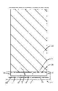
[0023] FIG. 1 is a schematic diagram of a mobile terminal
according to this
application;
[0024] FIG. 2 is a schematic diagram of an antenna according to
this application;
[0025] FIG. 3 is a schematic diagram of a current flow direction of the
antenna
shown in FIG. 2;
[0026] FIG. 4 is a schematic diagram of resonant coupling inside
an antenna
according to this application;
[0027] FIG. 5 is a schematic diagram of a current flow direction
of an antenna in
the prior art;
[0028] FIG. 6 is a schematic diagram of a characteristic current
on a typical circuit
board according to this application;
[0029] FIG. 7a is a schematic diagram of an embodiment of the
antenna according
to this application;
100301 FIG. 7b is a schematic diagram of an embodiment of the antenna
according
to this application;
[0031] FIG. 8 is a schematic diagram of an embodiment of an
antenna according to
this application;
[0032] FIG. 9 is a schematic diagram of an embodiment of an
antenna according to
this application;
[0033] FIG. 10 is a schematic diagram of an embodiment of a
mobile terminal
according to this application;
[0034] FIG. 11 is a schematic diagram of an embodiment of a
mobile terminal
according to this application; and
[0035] FIG. 12 is a schematic diagram of an embodiment of a mobile terminal
according to this application.
6
, .
CA 03067483 2019-12-16
. .
DESCRIPTION OF EMBODIMENTS
[0036] The technical solutions in this application are described
below with
reference to the accompanying drawings in the embodiments of this application.
Apparently, the described embodiments are merely some but not all of the
embodiments
of this application. All other embodiments obtained by a person of ordinary
skill in the
art based on the embodiments of this application without creative efforts
shall fall
within the protection scope of this application.
[0037] The mobile terminal in implementations of this application
may be any
device having a communication function, for example, an intelligent device
having a
network function such as a tablet computer, a mobile phone, an e-reader, a
remote
control, a notebook computer, a vehicle-mounted device, a web television, or a
wearable device. It can be understood that various mobile terminals are
usually
provided with wireless communication functions such as cellular (Cellular), a
wireless
local area network (WLAN), and Bluetooth (Bluetooth) based on a functional
requirement. Therefore, the mobile terminal is internally provided with an
antenna
configured to communicate with the outside.
[0038] Referring to FIG. 1, a mobile terminal 200 includes a
radiation portion 210,
a circuit board 220, a transceiver 230, and an antenna 100. Apart of the
radiation portion
210 and a part of the circuit board 220 jointly constitute a body of the
antenna 100. The
radiation portion 210 may be a frame of the mobile terminal 200, or may be a
metal
rear cover of the mobile terminal 200. When the radiation portion 210 is the
frame, for
example, in an embodiment shown in FIG. 1, a bottom part of the frame and an
edge of
the circuit board 220 jointly constitute the body of the antenna 100. When the
radiation
portion 210 is the metal rear cover, a metal belt similar to a frame may be
formed on an
edge of the metal rear cover by providing a slot, and similarly the metal belt
and the
edge of the circuit board 220 jointly constitute the body of the antenna 100.
[0039] The antenna 100 includes a feed point 101, and the
transceiver 230 is
electrically connected to the feed point 101 in the antenna 100. Therefore,
when the
antenna 100 operates, the transceiver 230 exchanges data with the outside
through the
7
CA 03067483 2019-12-16
antenna 100. Specifically, the transceiver 230 is a radio frequency
transceiver circuit
and is configured to feed an electromagnetic wave signal to the antenna 100.
[0040] Specifically, referring to FIG. 2, the antenna 100 includes a feed
stub 10, a
parasitic stub 20, a feed branch 11, a grounding branch 21, and a grounding
portion 30.
The circuit board 220 of the mobile terminal 200 includes a lateral side 221.
The
radiation portion 210 may be a part of a metal housing (including a frame and
a rear
cover) of the mobile terminal 200. For example, the radiation portion 210 is a
part of
the frame, or the radiation portion 210 may be apart close to an edge on the
metal rear
cover, and has a position close to that of the frame. A gap 40 is disposed
between the
radiation portion 210 and the lateral side 221. The circuit board 220 includes
a
grounding layer, and two ends of the radiation portion 210 on the lateral side
221 are
separately connected to the grounding layer. The grounding layer in the
circuit board
220 constitutes the grounding portion 30 of the antenna 100. It can be
understood that
a connection between the radiation portion 210 and the grounding portion 30
also
enables the gap 40 to form a closed-loop structure. The radiation portion 210
is provided
with an insulating slot 50. The insulating slot 50 divides the radiation
portion 210 into
the feed stub 10 and the parasitic stub 20. Therefore, for the antenna 100, a
body
structure of the antenna 100 includes the grounding portion 30 located inside
the lateral
side 221, the feed stub 10, and the parasitic stub 20. The feed stub 10 and
the parasitic
stub 20 are divided by the insulating slot 50. The gap 40 is encompassed by
the feed
stub 10, the parasitic stub 20, and the lateral side 221. It can be understood
that the gap
40 may be considered as a clearance area of the antenna 100.
[0041] The feed branch 11 is further disposed on the feed stub 10. The
feed branch
11 extends from the feed stub 10 to the gap 40. An end that is of the feed
branch 11 and
that is far away from the feed stub 10 is the feed point 101 of the antenna
100, and the
end that is of the feed branch 11 and that is far away from the feed stub 10
may extend
to the inside of the circuit board 220, and feeds the feed branch 11 through a
feed circuit
disposed on the circuit board 220. A grounding branch 22 extending to the gap
40 is
further disposed on the parasitic stub 20. The grounding branch 22 is
electrically
connected to the grounding portion 30. An end that is of the grounding branch
22 and
8
,
CA 03067483 2019-12-16
that is far away from the parasitic stub 20 may extended to the inside of the
circuit board
220, and the grounding branch 22 may be electrically connected to the
grounding
portion 30 through a grounding spring or may be electrically connected to the
grounding
portion 30 in a manner of welding.
[0042] During feeding at the feed point 101, a current is generated on the
feed
branch 11 and a low-frequency resonance stub is formed. Because the feed
branch 11
is connected to the feed stub 10, the feed stub 10 is also loaded with a
feeding current.
In addition, the feeding current is the smallest at the insulating slot 50,
and is the largest
at a position at which the feed stub 10 is connected to the grounding portion
30. Because
the current is the smallest and an electric field is strongest at the
insulating slot 50, the
current may be coupled to the parasitic stub 20. The current on the parasitic
stub 20 is
also the smallest at the insulating slot 50, and is the largest at a position
at which the
parasitic stub 20 is connected to the grounding portion 30. The feed branch 11
includes
a resonance because of the feeding current, and the grounding branch 21
includes a
parasitic resonance because of a parasitic current. In this design, when the
antenna 100
operates in a low frequency, two approximate resonance frequencies are
distributed on
the left and right of the insulating slot 50. The two resonance frequencies
are designed
through strong electric field coupling, and an induced current is excited at
the grounding
portion 30 after the feed branch 11 and the grounding branch 21 are coupled.
The
induced current passes through the grounding portion 30, the feed stub 10, and
the
parasitic stub 20 successively. To be specific, the induced current circulates
around the
gap 40 (refer to FIG. 3). A frequency of the induced current excited at the
grounding
portion 30 after the feed branch 11 and the grounding branch 21 are coupled is
a
frequency of a signal transmitted by the radiation portion 210 to the outside.
[0043] Referring to FIG. 4, in FIG. 4, a lateral axis represents a
frequency measured
in MHz, and a longitudinal axis represents a reflection coefficient
(reflection coefficient)
of the antenna measured in dB. It can be understood that an antenna bandwidth
is a
bandwidth of a frequency whose reflection coefficient is less than ¨6 dB. For
two
approximate resonance frequencies, a resonance frequency of a resonance
generated by
the feed branch 10 is 890 MHz, a resonance frequency of a resonance generated
by the
9
. .
CA 03067483 2019-12-16
,
parasitic stub 20 is 970 MHz, and a frequency connected between the two
resonances
is 930 MHz.
[0044] It should be noted that the induced current excited at the
grounding portion
30 after the feed stub 10 and the parasitic stub 20 are coupled is parallel to
the gap 40,
or is described as an induced current parallel to the lateral side 221. In the
prior art, the
feed stub 10 is not coupled to the parasitic stub 20 (refer to FIG. 5), and a
low-frequency
operating principle of an antenna 1000 in the prior art is as follows: A feed
point 1001
excites, on a grounding portion 300, an induced current that vertically flows
to a lateral
side 2021 and that gathers towards the feed point 1001. The current on the
grounding
portion 300 is the largest at the feed point 1001, and the induced current is
smaller when
being farther away from the feed point 1001. Provided that an antenna
clearance and an
antenna form are given, a resonance and efficiency of the antenna 1000 in the
prior art
depend on a length and a size of the grounding portion 300 perpendicular to
the lateral
side 2021. To be specific, an antenna resonance having an unbalanced 1/2
wavelength
include both a size of the grounding portion 300 perpendicular to the lateral
side 2021
and a size of a feed stub of a radiation portion 2100.
[0045] A current mode of coupling exciting of the antenna 100
provided in the
embodiments of this application on the feed stub 10 and the parasitic stub 20
is a first
current mode 001 shown in FIG. 6. FIG. 6 shows a strength distribution manner
of a
characteristic current of the antenna 100 in the first current mode 001. The
grounding
portion 30 is of a rectangular shape. The left of FIG. 6 is current
distribution of the
characteristic current on a short side of the grounding portion 30, and the
right of FIG.
6 is current distribution of the characteristic current on a long side of the
grounding
portion 30. It can be found that, in the first current mode 001, regardless of
whether the
lateral side 221 is located on the long side or the short side of the
grounding portion 30,
the characteristic current on the grounding portion 30 always appears in a
shape of being
the largest in the middle and being the smallest at two ends.
[0046] FIG. 5 shows a strength distribution manner of a
characteristic current of the
antenna in a second current mode 002 in the prior art, that is, a case in
which a current
direction of the antenna 1000 is perpendicular to the lateral side in the
prior art. With
CA 03067483 2019-12-16
reference to a status of feed exciting performed on the grounding portion 300
by the
feed point 1001 in the gap 400, it can be learned that, in the second current
mode 002
in which the current direction is perpendicular to the lateral side 2021,
exciting
performed on the grounding portion 300 by the feed point 1001 is just located
at a
position having a weakest characteristic current in the second current mode
002.
Consequently, the antenna 1000 does not form most effective exciting on the
grounding
portion 300 in the prior art, making excited low-frequency efficiency
relatively poor,
and a clearance area between an antenna stub and the grounding portion of the
antenna
usually needs to be enlarged for compensation.
[0047] Therefore, according to distribution of a characteristic current of
a feature
model of the grounding portion 30 according to this application, if a low
frequency of
the grounding portion 30 needs to be excited mostly effectively, a point
having a largest
characteristic current on the grounding portion 30 needs to be excited. To be
specific,
an exciting source of the antenna 100 needs to be located in an area of a
point having
largest current distribution in a current mode corresponding to the grounding
portion
30 for exciting. In the antenna 100 according to this application, the gap 40
is
encompassed by the radiation portion 210 and the lateral side 221 in the
antenna 100,
and the insulating slot 50 divides the radiation portion 210 into the feed
stub 10 and the
parasitic stub 20. It is considered as a current circulation path of the
antenna 100.
Further, in the antenna 100 according to this application, the feed branch 11
and the
grounding branch 21 extend into the gap 40 from the feed stub 10 and the
parasitic stub
20 separately. An end that is of the feed branch 11 and that is far away from
the feed
stub 10 is the feed point 101, and an end that is of the grounding branch 21
and that is
far away from the parasitic stub 20 is electrically connected to the grounding
portion
30, to maintain potential balance of the grounding branch 21. To be specific,
the feed
branch 11 is coupled to the grounding branch 21, to excite the grounding
portion 30. In
this case, the induced current generated on the grounding portion 30 is
parallel to the
lateral side 221 in the first current mode 001. However, the feed branch 11
and the
grounding branch 21 need to be located within a distance range that can
sufficiently
ensure coupling, so that the feed branch 11 is coupled to the grounding branch
21.
11
. .
CA 03067483 2019-12-16
. ,
Generally, the feed branch 11 and the grounding branch 21 are both relatively
close to
the insulating slot 50 and relatively far away from an end position of the gap
40. In this
way, in the first current mode 001, an exciting position of the induced
current excited
on the grounding portion 30 after the feed branch 11 and the grounding branch
21 are
coupled is away from the two end portions of the gap 40, so that the grounding
portion
30 is excited at a position having largest characteristic current distribution
in the first
current mode 001. To be specific, the feed branch 11 and the grounding branch
21 can
form a resonance to the current at a position having a relatively large
induced current,
so that the low frequency efficiency of the antenna 100 is higher and a
clearance area
needed by the antenna is smaller. In this way, the antenna 100 according to
this
application can obtain higher radiation efficiency and signal sending and
receiving
performance.
[0048] It can be understood that the mobile terminal may obtain a
better call effect
and a smaller area by using the antenna.
[0049] In an embodiment, the antenna 100 is applied to atypical circuit
board of a
mobile terminal. The circuit board 220 is a rectangle having a length of 150
mm and a
width of 75 mm. Because a low band of the antenna 100 includes a 617-960 MHz
band,
most low band signals in the prior art are covered. It can be understood that
the antenna
100 further includes LTE and GPS bands close to low frequencies, for example,
an LTE
B11/21/32 band (1427 MHz to 1511 MHz) and a GPS L1/L2/L5 band (1575.42
MHz/1227.6 MHz/1176.45 MHz).
[0050] In a specific implementation, the grounding portion 30,
the feed stub 10, and
the parasitic stub 20 jointly constitute electrical length that is a half of a
wavelength of
the operating frequency of the antenna, so that a resonance generated by the
grounding
portion 30, the feed stub 10, and the parasitic stub 20 excites an induced
current that
winds around the gap and that is a relatively large value. It can be
understood that when
the length of the gap is 1/4 of the wavelength of the operating frequency, the
length of
the lateral side 221 is also 1/4 of the wavelength of the transmit frequency,
and the
length of the radiation portion 210 is also roughly 1/4 of the wavelength of
the transmit
frequency. Because the radiation portion 210 surrounds the lateral side 221,
the length
12
. .
CA 03067483 2019-12-16
. .
of the radiation portion 210 is slightly greater than that of the lateral side
221. In an
embodiment, the radiation portion 210 and the lateral side 221 jointly
constitute 1/2 of
an asymmetric wavelength of a dipole of the antenna. Asymmetry herein means
that the
radiation portion 210 is slightly greater than the lateral side 221.
100511 In this embodiment, the insulating slot 50 is disposed at a midpoint
of a
length direction of the radiation portion 210, that is, a midpoint of a length
direction of
the gap 40. To be specific, an electrical length of the feed stub 10 is the
same as a length
and a size of the parasitic stub 20. When the insulating slot 50 is located at
a midpoint
position of the length direction of the gap 40, this helps to symmetrically
dispose the
feed branch 11 and the grounding branch 21 on two sides of the insulating slot
50, so
that when the feed branch 11 is coupled to the grounding branch 21, a midpoint
of the
coupling is just located at the gap 40, that is, a midpoint position of the
lateral side 221.
To be specific, a resonance exciting source of the antenna 100 is located at a
midpoint
position of the lateral side 221. It can be learned from the above description
that when
the antenna 100 is in the first current mode 001, a maximum value of the
characteristic
current of the antenna 100 is also located at the midpoint position of the
lateral side 221.
An exciting point of the grounding portion 30 after the feed branch 11 is
coupled to the
grounding branch 21 is located at a position having a largest exciting current
on the ,
grounding portion 30, so that better radiation efficiency can be obtained. It
can be
understood that to couple the feed branch 11 to the grounding branch 21, a
relative
distance between the feed branch 11 and the grounding branch 21 needs to
satisfy an
effective coupling effect between the feed branch 11 and the grounding branch
21.
100521 For the insulating slot 50, to ensure that the feed stub
10 is coupled to the
parasitic stub 20, the insulating slot 50 needs to be as narrow as possible,
and the
coupling between the feed branch 11 and the grounding branch 21 needs to be
more
matched, so that an antenna effect having better performance can be obtained.
Therefore,
a width range of the insulating slot 50, that is, a size in an extension
direction of the gap
40 is properly set to be greater than or equal to 0.2 mm and less than or
equal to 2 mm.
To be specific, a size of the insulating slot 50 in the length direction of
the radiation
portion 210 is properly set to be greater than or equal to 0.2 mm and less
than or equal
13
CA 03067483 2019-12-16
to 2 mm. This is different from an existing antenna design. This is because in
the
existing antenna design, a coupling relationship between the antenna stubs
mostly needs
to be weakened as much as possible, to avoid mutual influence between the
stubs.
Therefore, a wider antenna gap is provided in most mobile terminals in the
prior art.
However, in the solution of the antenna 100 according to this application, the
insulating
slot 50 needs to be as narrow as possible, so that the mobile terminal 200
including the
antenna 100 may have a smaller antenna split, improving appearance consistency
of the
mobile terminal 200.
[0053] It can be understood that the coupling between the feed branch 11
and the
grounding branch 21 may further be controlled through a capacitance generated
by two
parallel planes formed by the insulating slot 50, that is, a cross-sectional
area of the
radiation portion 210 cut by the insulating slot 50. A same effect as that of
adjusting the
width of the insulating slot 50 can be realized by changing a cross-sectional
area of the
feed stub 10 and the parasitic stub 20 at the insulating slot 50, to adjust
the coupling
between the feed branch 11 and the grounding branch 21.
[0054] An embodiment is shown in FIG. 7a, and the insulating slot 50 in
the
embodiment shown in FIG. 7a includes a suspension section 51 made of a
conductive
material and a separation slot 52 on two sides of the suspension section 51.
It can be
understood that the suspension section 51 is located between the feed stub 10
and the
parasitic stub 20. An insulating separation slot 52 is disposed between the
suspension
section 51 and the feed stub 10 and between the suspension section 51 and the
parasitic
stub 20. To be specific, the suspension section 51 is a section on the
radiation portion
210, the suspension section 51 is located between the feed stub 10 and the
parasitic stub
20, and the suspension section 51 and the separation slot 52 at two ends of
the
suspension section 51 jointly form the insulating slot 50, so that the feed
stub 10 and
the parasitic stub 20 are divided. The feed stub 10 passes through the
separation slot 52
to feed the suspension section 51, and passes through the separation slot 52
to feed the
parasitic stub 20 through the suspension section 51. After obtaining the
parasitic current
through the suspension section 51, the parasitic stub 20 is coupled to the
feed stub 10,
to provide a resonance exciting for the grounding portion 30. The suspension
section
14
. .
CA 03067483 2019-12-16
. .
51 may be disposed as an external key or interface of the mobile terminal 200,
such as,
a structure of a charging interface or a USB interface of the mobile terminal
200. When
the radiation portion 210 is a frame or a housing, this type of interface is
mostly
disposed on the radiation portion 210, and this type of interface is mostly
directly
formed as an opening on the radiation portion 210. A shape change of the
radiation
portion 210 at this type of interface is relatively large. Therefore, directly
disposing the
insulating slot 50 herein does not help a resonance design of the antenna 100.
Instead,
this type of key or interface is independently disposed as the suspension
section 51, and
the suspension section 51 is separated from the feed stub 10 and the parasitic
stub 20
by the separation slot 52, so that the feed stub 10 and the parasitic stub 20
are both
conductors of a relatively consistent shape, helping to simplify a model of
the antenna
100 and realize more accurate feature matching design.
[0055] In another aspect, because the insulating slot 50 is at a
midpoint position of
the gap 40, and the suspension section 51 interferes with coupling between the
feed
branch 11 and the grounding branch 21 to some extent, the coupling becomes
weak. In
this case, the feed branch 11 and the grounding branch 21 both need to be
disposed near
the insulating slot 50. An end that is of the gap 40 and at which the feed
stub 10 is
electrically connected to the grounding portion 30 is defmed as a first end
41, and the
other end of the gap 40 is defined as a second end 42. It can be understood
that the
second end 42 is close to a position at which the parasitic stub 20 is
electrically
connected to the grounding portion 30. The feed branch 11 and the grounding
branch
21 being disposed near the insulating slot 50 means that the feed branch 11 is
closer to
the insulating slot 50 relative to the first end 41, and the grounding branch
21 is also
closer to the insulating slot 50 relative to the second end 42.
[0056] In an embodiment, a length range of the suspension section 51, that
is, a size
of the suspension section 51 in a length direction of the radiation portion
210, is set to
be greater than or equal to 12 mm and less than or equal to 18 mm, and a
length range
of the separation slot 52, that is, a size of the separation slot 52 in the
length direction
of the radiation portion 210, is set to be greater than or equal to 0.2 mm and
less than
or equal to 1.5 mm. The length direction of the radiation portion 210 is a
direction in
CA 03067483 2019-12-16
which the radiation portion 210 extends from the feed stub 10 to the parasitic
stub 20.
This setting can ensure that the length of the suspension section 51 matches
sizes of
most keys or interfaces, and further ensure effective coupling between the
grounding
branch 21 and the feed branch 11.
[0057] A cyclic current is generated at the gap 40. In addition, a current
also passes
through the feed branch 11 and the grounding branch 21. In an embodiment, to
ensure
effective coupling between the grounding branch 21 and the feed branch 11, a
length
by which the grounding branch 21 extends to the gap 40 may be set to 1/4 of a
wavelength of an operating frequency of the antenna, a range of a length by
which the
feed branch 11 extends to the gap 40 is greater than or equal to 1/6 of the
wavelength
of the operating frequency ofthe antenna, and less than or equal to 1/8 of the
wavelength
of the operating frequency of the antenna, and a length by which the grounding
branch
extends to the gap is 1/4 of the wavelength of the operating frequency of the
antenna.
[0058] Specifically, when positions of the feed branch 11 and the first
end 41 are
fixed, an electrical length of the feed branch 11 is related to a distance
between the feed
point 101 and the insulating slot 50. Generally, in the embodiment shown in
FIG. 7a,
when the feed point 101 of the feed branch 11 is close to the insulating slot
50, the
electrical length of the feed branch 11 is 1/8 to 1/6 (the range includes an
endpoint) of
the wavelength of the operating frequency of the antenna; when the feed point
101 of
the feed branch 11 is far away from the insulating slot 50, the electrical
length of the
feed branch 11 may be understood as 1/4 of the wavelength of the operating
frequency
of the antenna. A relative distance between the feed branch 11 and the
insulating slot
50 and a length between the feed point 101 and the first end 41 may be
adjusted to
control and adjust the electrical length of the feed branch 11.
[0059] In an embodiment, because a length of the lateral side 221 is a
fixed value,
when a feeding current at the feed point 101 emits a signal of a corresponding
resonance
frequency, the grounding branch 21 generates a parasitic current of another
resonance
frequency. To ensure that impedance of the feeding current on the feed branch
11 and
the parasitic current on the grounding branch 21 match each other, the
grounding branch
.. 21 may further be connected to a parasitic frequency modulation apparatus
22 in series
16
CA 03067483 2019-12-16
at the grounding portion 30. The parasitic frequency modulation apparatus 22
is located
between the grounding branch 21 and the grounding portion 30. It can be
understood
that a frequency modulation component common in the art, for example, a
component
such as a capacitor or an inductor may be used as the parasitic frequency
modulation
apparatus 22.
[0060] Correspondingly, the feed stub 10 may alternatively be provided
with a feed
frequency modulation branch 12. The feed frequency modulation branch 12 is in
an
extending direction in which the parasitic stub 21 faces the feed stub 11,
that is, the feed
frequency modulation branch 12 is located between the feed stub 11 and the
first end
41. The feed frequency modulation branch 12 also extends to the gap 40, and
the feed
frequency modulation branch 12 is electrically connected to the grounding
portion 30,
to perform a grounding function of the feed stub 10.
[0061] In an embodiment, a feed frequency modulation apparatus 121 may be
alternatively disposed between the feed frequency modulation branch 12 and the
grounding portion 30, and is configured to adjust a frequency of the feed stub
10. It can
be understood that the feed frequency modulation apparatus 121 may
alternatively be a
component such as a capacitor or an inductor.
[0062] In terms of a typical circuit board of a mobile terminal, the
circuit board 220
in this embodiment of this application is a rectangle having a length of 150
mm and a
width of 75 mm. When the lateral side 221 is on a width (75 mm) side of the
circuit
board, an extended length of the lateral side 221 in this direction does not
exceed a
maximum of 75 mm. For a low-frequency resonance of the antenna, the lateral
side 221
is required to have a relatively large length to match an electrical length of
a 1/4
wavelength. Therefore, when the lateral side 221 is on a single edge of the
mobile
terminal 200, and a length of the single edge cannot sufficiently match the
1/4
wavelength required by a low frequency of the mobile terminal 200, the lateral
side 221
needs to be extended. That is, the length of the lateral side 221 is increased
to match the
electrical length required by the frequency. Correspondingly, extension of the
lateral
side 221 drives the radiation portion 210 to extend, and the gap 40
correspondingly
increases as the lateral side 221 and the radiation portion 210 extend (as
shown in FIG.
17
CA 03067483 2019-12-16
8). The lateral side 221 is in a shape of a folded side, the lateral side 221
in the shape
of a folded side includes a first segment 401 and a second segment 402 that
intersect
with each other, and an end of the first segment 401 and an end of the second
segment
402 coincide. Correspondingly, the first end 41 of the gap 40 is located at an
end of the
first segment 401, and the second end 42 is located at an end of the second
segment 402.
The feed stub 10 or the parasitic stub 20 also bends synchronously along with
the lateral
side 221, to maintain a consistent cross-sectional width of the gap 40 in a
length
extension direction. After the shape of the gap 40 changes, a current cyclic
loop of the
antenna 100 during feeding still proceeds around the gap 40. In this case, a
start position
of an induced current of the antenna 100 depends on a coupling position of the
feed
stub 10 and the parasitic stub 20. To be specific, when the coupling position
of the feed
stub 10 and the parasitic stub 20 appears in the first segment 401, the start
position of
the induced current on the grounding portion 30 is the coupling position
corresponding
to the first segment 401. When the coupling position of the feed stub 10 and
the parasitic
stub 20 appears in the second segment 402, the start position of the induced
current on
the grounding portion 30 is the coupling position corresponding to the second
segment
402. It can be understood that regardless of any position of the induced
current on the
grounding portion 30, a flowing path of the induced current proceeds around
the gap
40. In this case, a length sum of the first segment 401 and the second segment
402 is
set to be equal to a 1/4 wavelength of a low-frequency midpoint of the mobile
terminal
200, so that the antenna 100 can effectively generate a low-frequency
resonance.
[0063] In this disposing manner, the antenna 100, including the position
of the
insulating slot 50 in the mobile terminal 200, is disposed relatively
flexibly. However,
in an existing antenna technology, radiation bodies of a mobile terminal are
mostly
metal frames and include a metal rear cover, and radiation is implemented by
providing
a gap on the frame. In this disposing manner, when a user makes a call in a
head-hand
mode, because a hand of the person holds the metal frame and the metal rear
cover,
efficiency attenuation of the antenna is caused. Particularly, when the hand
holds a gap
of the metal frame, performance attenuation of the antenna is serious,
deteriorating
communication performance.
18
CA 03067483 2019-12-16
[0064] Therefore, an antenna split is provided at a bottom portion of
most
rectangular mobile terminals 200, to avoid a direct contact between a human
hand and
the split. In this case, an antenna feed point excites a current of a longer
side direction
of a circuit board to perform radiation, that is, the second current mode 002
of this
application. It can be learned from the above descriptions that in the second
current
mode 002, a characteristic current of the antenna 100 is just a smallest value
at a position
closest to the feed point 101. In this way, excited antenna radiation
efficiency is lower.
In an embodiment, because a split of the mobile terminal in a head-hand mode
is still
close to a position at which the user holds the mobile terminal, attenuation
of the
antenna in the head-hand mode is more serious in the prior art. Generally, a
low
frequency reduction of the antenna in the prior art is at least greater than 6
dB.
[0065] However, for the antenna 100 of this application, on the one hand,
because
a position of the antenna 100 of this application is not limited by a
wavelength of a low
frequency, the antenna 100 is relatively flexibly disposed. In theory, the
antenna 100
may be disposed at any position around the mobile terminal 200.
Correspondingly, the
insulating slot 50 may also be disposed at any position of an edge of the
mobile terminal
200. Coverage of the antenna by a palm of a user in the head-hand mode may be
reduced
to the lowest. On the other hand, because the antenna 100 of this application
uses the
first current mode 001 to perform exciting, exciting efficiency of the antenna
100 is
higher, and a signal attenuation problem of the antenna 100 in the head-hand
mode can
be avoided to a great extent. It can be learned from a test that when the
insulating slot
50 is disposed at a bottom position of the mobile terminal 200, a low
frequency
reduction of the antenna 100 of this application in the head-hand mode is
controlled to
be within 3 dB.
[0066] It should be noted that the antenna 100 is disposed at a bottom
portion of the
mobile terminal 200. In this embodiment of this application, this is defined
as follows:
the lateral side 221 is located at a bottom end of a default display picture
of the display
surface 240 of the mobile terminal 200, that is, a bottom end of the mobile
terminal 200
when the user watches the mobile terminal 200 from a font view. When a typical
circuit
board 220 of a rectangular shape having a length of 150 mm and a width of 75
mm is
19
, .
CA 03067483 2019-12-16
. .
used for the mobile terminal 200, when the user holds the mobile terminal 200
and
enters a head-hand mode, a bottom position of the mobile terminal 200 usually
is not
covered and is in a relative open and free status. Therefore, the antenna 100
is disposed
at the bottom end ofthe mobile terminal 200, to facilitate signal receiving of
the antenna.
[0067] According to another aspect, in existing mobile terminal products,
structures
such as a charging interface and a USB interface are mostly disposed at a
bottom portion
of the mobile terminal. In an embodiment in which the insulating slot 50 in
the antenna
100 of this application further includes the suspension section 51, interface
design of
the mobile terminal 200 of this application is also facilitated.
[0068] An embodiment is shown in FIG. 9. A folded side of the lateral side
221
further includes a third segment 403. The third segment 403 is located at an
end that is
of the first segment 401 and that is far away from the second segment 402, and
the third
segment 403 also intersects with the first segment 401. To be specific, the
first segment
401 is connected between the second segment 402 and the third segment 403, and
the
second segment 402 and the third segment 403 bend in a same direction from the
first
segment 401. Similarly, the feed stub 10 or the parasitic stub 20 bends
synchronously
along with the lateral side 221, and the feed stub 10 or the parasitic stub 20
also includes
two intersected shapes, to maintain a consistent cross-section width of the
gap 40 in a
length extension direction. It can be understood that the first end 41 of the
gap 40 in
this embodiment is located at an end that is of the third segment 403 and that
is far away
from the first segment 401, and the second end 42 is located at an end that is
of the
second segment 402 and that is far away from the first segment 401. With
introduction
of the third segment 403, a length of the gap 40 can further be extended. In
this way,
when a length of a lateral side of the grounding portion 30 in a specific
direction is
insufficient, introduction of the third segment 403 helps, through matched
design of the
third segment 403 and the second segment 402, to dispose the insulating slot
50 at a
position of a lateral frame that is of the mobile terminal 200 and that
corresponds to the
lateral side wall. Further, when a length of the third segment 403 is the same
as that of
the second segment 402, the insulating slot 50 may be located in a middle
portion of a
lateral frame of the mobile terminal 200. When the structure such as the
charge interface
, .
CA 03067483 2019-12-16
. .
or the USB interface is disposed on the mobile terminal 200, a corresponding
interface
structure is disposed on a lateral side of the mobile terminal 200, for
example, a middle
portion of a bottom side.
[0069] It should be noted that the intersection between the first
segment 401 and
the second segment 402 and the intersection between the third segment 403 and
the first
segment 401 is vertical intersection shown in FIG. 9. In some other
embodiments, the
intersection between the first segment 401 and the second segment 402 and the
intersection between the third segment 403 and the first segment 401 may be
disposed,
based on a different shape of the circuit board 220 or a different shape of
the radiation
portion 210, as intersection of any other angles or shapes such as
intersection of curves
and intersection of a plurality of straight line segments. As long as the
length of the gap
40 can be extended effectively to match a wavelength required by a resonance
frequency,
the technical solutions claimed by this application can be implemented.
[0070] Referring to the embodiment shown in FIG. 7b again and
with reference to
features of the two embodiments shown in FIG. 7a and FIG. 9, the lateral side
221 of
the antenna 100 includes the second segment 402 and the third segment 403, and
the
insulating slot 50 also includes the suspension section 50 and the separation
slot 52.
The embodiment shown in FIG. 7b is applicable to a case in which on a shorter
lateral
side of the mobile terminal 200, an interface needs to be disposed at an
opening
provided at a middle position of the shorter lateral side.
[0071] In an embodiment shown in FIG. 10, the antenna 100 is
disposed on both a
top surface and a bottom surface of the mobile terminal 200, and the two
antennas 100
may be in a same frequency band or may be set to be in different frequency
bands that
can switch automatically. A communication capability of the mobile terminal
200 can
be further strengthened by disposing the two antennas 100.
[0072] For ease of understanding, the embodiment of the antenna
100 of this
application is described by using a typical circuit board of a mobile
terminal. However,
it can be learned from the specification of this application that the mobile
terminal 200
of this application is not limited to a mobile phone, and may further include
an
intelligent device having a network function such as a tablet computer, an e-
reader, a
21
CA 03067483 2019-12-16
remote control, a notebook computer, a vehicle-mounted device, a web
television, or a
wearable device. Therefore, the circuit board 220 of the mobile terminal 200
of this
application may further have any size that can match the above product
structure. The
antenna 100 of this application may further be disposed at any edge position
of the
mobile terminal 200 according to actual situations. For example, in the
embodiment
shown in FIG. 11, the mobile terminal 200 is a tablet computer, and the user
easily holds
two sides of the tablet computer with both the left hand and the right hand
when holding
the tablet computer. In this case, the antenna 100 is disposed at both a top
portion and
a bottom portion of the mobile terminal 200, so that a better communication
effect can
be implemented when the user holds the tablet computer. It can be understood
that the
antenna 100 is located at a position of a longer lateral side of the mobile
terminal 200,
and this is different from the above embodiment in which the antenna 100 is
located at
a position of a shorter lateral side of the mobile terminal 200.
[0073] In the above embodiments, the radiation portion 210 of the mobile
terminal
200 may be a metal side frame structure of the mobile terminal 200, or may be
a metal
middle frame structure of the mobile terminal 200. In this case, a rear cover
250 of the
mobile terminal 200 is properly made of a non-conductive material such as
glass or
plastic, and the radiation portion 210 is relatively independent and surrounds
at least a
segment of the circuit board 220, so that the technical solution of the
antenna 100 of
this application is implemented. However, in some embodiments of the rear
cover 250
using only a metal, the method shown in FIG. 12 may be used. A circle of
separation
251 is disposed on the rear cover 250 of the mobile terminal 200, and an edge
of the
rear cover 250 is separated by the separation 251 to form a segment of the
radiation
portion 210, where a part is used as the radiation portion 210 in the antenna
100 for
radiation.
[0074] In some other embodiments, the rear cover 250 is made of a non-
conductive
material, the radiation portion 210 is disposed in the rear cover 250 in a
manner of laser
direct structuring (LDS), insert molding (insert molding), or the like, and is
in
communication with the grounding portion 30 through the rear cover 250, so
that a
technical effect of the antenna of this application can be realized similarly.
Alternatively,
22
, .
CA 03067483 2019-12-16
. .
the radiation portion 210 is a flexible printed circuit board (FPC)
electrically connected
to the grounding portion 30.
[0075] The foregoing implementations are not intended to limit
the protection scope
of the technical solutions. Any modification, equivalent replacement, and
improvement
made without departing from the principle of the foregoing implementations
shall fall
within the protection scope of the technical solutions.
23