Note: Descriptions are shown in the official language in which they were submitted.
CA 03070035 2020-01-15
WO 2019/034708
PCT/EP2018/072153
ISOLATION DEVICE FOR ELECTROSURGICAL APPARATUS
FIELD OF THE INVENTION
The invention relates to electrosurgical apparatus in
which radiofrequency energy is used to treat biological
tissue. In particular, the invention relates to surgical
apparatus capable of generating radiofrequency (RF) energy for
cutting tissue, It may be used in as part of a surgical
apparatus which also delivers microwave frequency energy for
haemostasis (i.e. sealing broken blood vessels by promoting
blood coagulation).
BACKGROUND TO THE INVENTION
Surgical resection is a means of removing sections of
organs from within the human or animal body. Such organs may
be highly vascular. When tissue is cut (divided or
transected) small blood vessels called arterioles are damaged
or ruptured. Initial bleeding is followed by a coagulation
cascade where the blood is turned into a clot in an attempt to
plug the bleeding point. During an operation, it is desirable
for a patient to lose as little blood as possible, so various
devices have been developed in an attempt to provide blood
free cutting. For endoscopic procedures, it is also
undesirable for a bleed to occur and not to be dealt with as
soon as quickly as possible, or in an expedient manner, since
the blood flow may obscure the operator's vision, which may
lead to the procedure needing to be terminated and another
method used instead, e.g. open surgery.
Electrosurgical generators are pervasive throughout
hospital operating theatres, for use in open and laparoscopic
procedures, and are also increasingly present in endoscopy
suites. In endoscopic procedures the electrosurgical accessory
is typically inserted through a lumen inside an endoscope.
Considered against the equivalent access channel for
laparoscopic surgery, such a lumen is comparatively narrow in
bore and greater in length. In the case of a bariatric patient
the surgical accessory may have a length of 300 mm from handle
CA 03070035 2020-01-15
WO 2019/034708
PCT/EP2018/072153
2
to RF tip, whereas the equivalent distance in a laparoscopic
case can be in excess of 2500 mm.
Instead of a sharp blade, it is known to use
radiofrequency (RF) energy to cut biological tissue. The
method of cutting using RF energy operates using the principle
that as an electric current passes through a tissue matrix
(aided by the ionic contents of the cells and the
intercellular electrolytes), the impedance to the flow of
electrons across the tissue generates heat. When an RF voltage
is applied to the tissue matrix, enough heat is generated
within the cells to vaporise the water content of the tissue.
As a result of this increasing desiccation, particularly
adjacent to the RF emitting region of the instrument (referred
to herein as an RF blade) which has the highest current
density of the entire current path through tissue, the tissue
adjacent to the cut pole of the RF blade loses direct contact
with the blade. The applied voltage then appears almost
entirely across this void which ionises as a result, forming a
plasma, which has a very high volume resistivity compared to
tissue. This differentiation is important as it focusses the
applied energy to the plasma that completed the electrical
circuit between the cut pole of the RF blade and the tissue.
Any volatile material entering the plasma slowly enough is
vaporised and the perception is therefore of a tissue
dissecting plasma.
GB 2 486 343 discloses a control system for an
electrosurgical apparatus which delivers both RF and microwave
energy to treat biological tissue. The energy delivery
profile of both RF energy and microwave energy delivered to a
probe is set based on sampled voltage and current information
of RF energy conveyed to the probe and sampled forward and
reflected power information for the microwave energy conveyed
to and from the probe.
GB 2 522 533 discloses an isolating circuit for an
electrosurgical generator arranged to produce radiofrequency
(RF) energy and microwave energy for treating biological
tissue. The isolating circuit comprises a tunable waveguide
isolator at a junction between the microwave channel and
signal combiner, and can include a capacitive structure
between a ground conductor of the signal combiner and a
CA 03070035 2020-01-15
WO 2019/034708
PCT/EP2018/072153
3
conductive input section of the waveguide isolator to inhibit
coupling of the RF energy and leakage of the microwave energy.
SUMMARY OF THE INVENTION
At its most general, the present invention provides a
combined isolator-diplexer device for supplying radiofrequency
(RF) electromagnetic (EM) energy and microwave EM energy
obtained from separate source to a probe via a common signal
pathway. The invention combines into a single unit all the
necessary components to isolate the microwave and RF channels
from one another whilst providing a high withstanding voltage
(e.g. greater than 10 kV).
The invention improves upon the structure disclosed in GB
2 522 533 by providing the necessary isolation with a
plurality of series-connected capacitive structure integrally
formed with a waveguide isolator that assists in reducing
capacitive coupling across the isolation barrier.
According to the invention, there is provided a combined
isolator-diplexer device comprising: a combining circuit
having a first input connectable to receive radiofrequency
(RF) electromagnetic (EM) radiation having a first frequency
from an RF channel, a second input connectable to receive
microwave EM radiation having a second frequency that is
higher than the first frequency from a microwave channel, and
an output in communication with the first and second inputs
for conveying the RF EM radiation and the microwave EM
radiation to a common signal pathway, and a waveguide isolator
connected to isolate the microwave channel from the RF EM
radiation, wherein the waveguide isolator comprises: a
conductive input section, a conductive output section, a
conductive intermediate section, the intermediate section
having a first end which mates with the input section, and a
second end which mates with the output section, a first DC
isolation barrier arranged between the input section and the
intermediate section, and a second DC isolation barrier
arranged between the intermediate section and the output
section, wherein the input section, intermediate section and
output section together enclose a waveguide cavity, wherein
the output from the combining circuit includes a signal
conductor and a ground conductor, and wherein the first DC
CA 03070035 2020-01-15
WO 2019/034708
PCT/EP2018/072153
4
isolation barrier and the second DC isolation barrier provide
a pair of series-connected capacitive structures between the
ground conductor of the output from the combining circuit and
the conductive input section of the waveguide isolator, the
capacitive structure being arranged to inhibit coupling of the
RF EM energy and leakage of the microwave EM energy.
By providing a plurality (preferably a pair) of
capacitive elements connected in series within the structure
of the waveguide isolator itself, the overall capacitance can
be reduced without disturbing the transmission of microwaves
to the output or allowing unacceptable level of microwave
radiation or leakage.
The input section, intermediate section and output
section may be disposed in sequence along a longitudinal
direction, wherein the intermediate section overlaps in the
with the input section in the longitudinal direction at the
first DC isolation barrier, and wherein the intermediate
section overlaps in the with the output section in the
longitudinal direction at the second DC isolation barrier.
These regions of overlap provide two capacitive sections. The
intermediate section is arranged to ensure that the two
capacitive sections are spaced apart at or around a multiple
of a half guide-wavelength at the microwave frequency in the
intermediate section so that reflection of microwave energy
due to the change in diameter at the joints between sections
is cancelled. The extent of the longitudinal overlap between
the intermediate section and the input and output sections
respectively may be restricted by a pair of spacer elements.
The may be a first spacer element mounted between the
intermediate section and the input section and a second spacer
element mounted between the intermediate section and the
output section. The spacers may be mounted within recesses
formed in the input section and output section, such that they
abut a facing edge of the intermediate section. The spacer
elements may be formed from an insulating plastic, such as
Delrin0 or polyvinylchloride (PVC). If the waveguide is
cylindrical, the spacer elements may each comprise an annular
sleeve mounted over the distal end of one of the input or
output sections of the waveguide isolator. The outer surface
of the sleeves may be flush with the outer surface of the
input and output sections.
CA 03070035 2020-01-15
WO 2019/034708
PCT/EP2018/072153
The longitudinal length of the overlap between the inner
section and outer section and the respective portions of the
intermediate section is preferably at or around an odd number
of quarter wavelengths (usually one quarter wavelength) at the
5 microwave frequency.
An insulating layer may be disposed in each overlapping
region, i.e. between the input section and the intermediate
section at the first DC isolation barrier, and between the
output section and the intermediate section at the second DC
isolation barrier. A common insulating layer may be provided,
i.e. one insulating layer may extend between the overlapping
regions, e.g. under or through the intermediate section.
The insulating layer may have a thickness (e.g. radial
thickness if the waveguide is cylindrical) that is selected to
be either as thin as possible to minimise microwave leakage.
By providing a pair of capacitive structures, this layer can
be made thinner without increasing the capacitance to unwanted
levels.
The output connected to the common signal pathway may
includes an output probe mounted on the output section of the
waveguide isolator. The output probe may have a first
coupling conductor extending into the waveguide isolator to
couple the microwave EM energy therefrom. Similarly, the
second input may include an input probe mounted on the input
section of the waveguide isolator. The input probe may have a
second coupling conductor extending into the waveguide
isolator to couple the microwave EM energy into the cavity.
The first coupling conductor and second coupling conductor may
extend in a direction that is orthogonal to the longitudinal
direction. In one example, the first coupling conductor and
second coupling conductor may extend into the waveguide cavity
from opposite directions.
The first input may include an RF connector mounted on
the waveguide isolator. The RF connector may have a signal
conductor that extends into the waveguide cavity to
electrically contact the coupling conductor of the output
probe. The signal conductor may extend in the longitudinal
direction, and may be positioned to substantially align with
an equipotential of the microwave EM energy within the
waveguide isolator. Aligning the signal conductor in this way
CA 03070035 2020-01-15
WO 2019/034708
PCT/EP2018/072153
6
means that the amount of microwave EM energy that can leak
into the RF connector is minimal.
However, as a further barrier to leakage, the RF
connector may comprise a coaxial filter connected to the
output section and configured to inhibit microwave EM energy
from leaking out of the waveguide isolator through the signal
conductor of the RF connector. The coaxial filter may
comprise a two section re-entrant coaxial filter.
The waveguide isolator may comprise an adjustable
impedance. For example, it may comprise a plurality of tuning
stubs that are adjustably insertable into the waveguide cavity
along the longitudinal direction. The plurality of tuning
stubs may comprise a first tuning stub insertable through an
end face of the input section, and a second tuning stub
insertable through an end face of the output section. If the
waveguide cavity is cylindrical, the tuning stubs may lie on
the axis of the cylinder.
In another aspect, the invention may provide an
electrosurgical apparatus for resection of biological tissue,
the apparatus comprising: a radiofrequency (RF) signal
generator for generating RF electromagnetic (EM) radiation
having a first frequency; a microwave signal generator for
generating microwave EM radiation having a second frequency
that is higher than the first frequency; a probe arranged to
deliver the RF EM radiation and the microwave EM radiation
separately or simultaneously from a distal end thereof; and a
feed structure for conveying the RF EM radiation and the
microwave EM radiation to the probe, the feed structure
comprising an RF channel for connecting the probe to the RF
signal generator, and a microwave channel for connecting the
probe to the microwave signal generator, wherein the RF
channel and microwave channel comprise physically separate
signal pathways from the RF signal generator and microwave
signal generator respectively, wherein the feed structure
includes an isolator-diplexer device comprising: a combining
circuit having a first input connected to receive the RF EM
radiation from the RF channel, a second input connected to
receive the microwave EM radiation from the microwave channel,
and an output in communication with the first and second
inputs for conveying the RF EM radiation and the microwave EM
radiation to the probe along a common signal pathway, and a
CA 03070035 2020-01-15
WO 2019/034708
PCT/EP2018/072153
7
waveguide isolator connected to isolate the microwave channel
from the RF EM radiation, wherein the waveguide isolator
comprises: a conductive input section, a conductive output
section, a conductive intermediate section, the intermediate
section having a first end which mates with the input section,
and a second end which mates with the output section, a first
DC isolation barrier arranged between the input section and
the intermediate section, and a second DC isolation barrier
arranged between the intermediate section and the output
section, wherein the input section, intermediate section and
output section together enclose a waveguide cavity, wherein
the output from the combining circuit includes a signal
conductor and a ground conductor, and wherein the first DC
isolation barrier and the second DC isolation barrier provide
a pair of series-connected capacitive structures between the
ground conductor of the output from the combining circuit and
the conductive input section of the waveguide isolator, the
capacitive structure being arranged to inhibit coupling of the
RF EM energy and leakage of the microwave EM energy.
This aspect of the invention may be combined with any or
all of the components (either individually or in any
combination) described below with reference to the
electrosurgical apparatus 400 of Fig. 1. For example, the RF
channel and microwave channel may include any or all of the
components of the RF channel and microwave channel
respectively described below. The microwave channel may
include a circulator for separating a reflected signal on the
microwave channel from a forward signal. In an alternative
embodiment, a directional coupler may be used for the same
purpose. In practice, the circulator or directional coupler
will exhibit imperfect isolation, which in turn affects the
reflected signal that is actually received at the detector.
The isolator-diplexer device may comprise an adjustable
impedance capable of compensating for this imperfect isolation
as well as optimising return loss and transmission in the
waveguide isolator.
The apparatus may be configured to supply energy for
cutting and coagulating tissue simultaneously (e.g. a mixed or
blend mode) or may be operated independently, whereby the RF
and microwave energy is delivered to the probe under manual
user control (e.g. based on the operation of a footswitch
CA 03070035 2020-01-15
WO 2019/034708
PCT/EP2018/072153
8
pedal) or automatically based on measured phase and/or
magnitude information from the RF and/or microwave channel.
The system may be used to perform tissue ablation and cutting.
In the instance where microwave and RF energy are delivered
simultaneously, either or both RF and microwave energy
returned to the respective generators may be used at high
power or low power to control the energy delivery profile. In
this instance, it may be desirable to take measurements during
the OFF time when the energy delivery format is pulsed.
The distal end of the probe may comprise a bipolar
emitting structure comprising a first conductor spatially
separated from a second conductor, the first and second
conductors being arranged to act: as active and return
electrodes respectively to convey the RF EM radiation by
conduction, and as an antenna or transformer to facilitate
radiation of the microwave EM energy. Thus, the system may be
arranged to provide a local return path for RF energy. For
example, the RF energy may pass by conduction through the
tissue separating the conductors, or a plasma may be generated
in the vicinity of the conductors to provide the local return
path. RF tissue cutting may be produced by a fixed dielectric
material separating the first and second conductors, where the
thickness of the dielectric material is small, i.e. less than
1 mm and the dielectric constant high, i.e. greater than that
of air.
The invention may be particularly suitable in
gastrointestinal (GI) procedures, e.g. to remove polyps on the
bowel, i.e. for endoscopic sub-mucosal resection. The
invention may also lend itself to precision endoscopic
procedures, i.e. precision endoscopic resection, and may be
used in ear, nose and throat procedures and liver resection.
The term "conductive" is used herein to mean electrically
conductive, unless the context dictates otherwise.
The first frequency may be a stable fixed frequency in
the range 10 kHz to 300 MHz and the second frequency may be a
stable fixed frequency in the range 300 MHz to 100 GHz. The
first frequency should be high enough to prevent the energy
from causing nerve stimulation and low enough to prevent the
energy from causing tissue blanching or unnecessary thermal
margin or damage to the tissue structure. Preferred spot
frequencies for the first frequency include any one or more
CA 03070035 2020-01-15
WO 2019/034708
PCT/EP2018/072153
9
of: 100 kHz, 250 kHz, 400 kHz, 500 kHz, 1 MHz, 5 MHz.
Preferred spot frequencies for the second frequency include
915 MHz, 2.45 GHz, 5.8 GHz, 14.5 GHz, 24 GHz. Preferably the
second frequency is at least an order of magnitude (i.e. at
least 10 times) higher than the first frequency.
BRIEF DESCRIPTION OF THE DRAWINGS
Embodiments of the invention are described in detail
below with reference to the accompanying drawings, in which:
Fig. 1 is an overall schematic system diagram of an
electrosurgical apparatus in which the present invention may
be used;
Fig. 2 is a schematic diagram of a known example of an
isolating circuit that can be used in an electrosurgical
apparatus;
Fig. 3 is a schematic cut-away illustration of the
conductive components of a combined isolator-diplexer that is
an embodiment of the invention;
Fig. 4 is a schematic cut-away illustration of the
insulating components in the combined isolator-diplexer that
is an embodiment of the invention;
Fig. 5 is schematic cut-away illustration of an RF
diplexer configuration for the combined isolator-diplexer that
is an embodiment of the invention;
Fig. 6 is a cut-away diagram of a simulation model of the
combined isolator-diplexer that is an embodiment of the
invention;
Fig. 7 is a graph showing predicted transmission and
reflection parameters obtained using the simulation model of
the combined isolator-diplexer that is an embodiment of the
invention;
Fig. 8 is a cut-away section of a simulation model of a
microwave filter mounted at an RF port of the combined
isolator-diplexer that is an embodiment of the invention; and
Fig. 9 is a graph showing predicted transmission and
reflection parameters for the microwave filter obtained using
the simulation model of Fig. 8.
DETAILED DESCRIPTION; FURTHER OPTIONS AND PREFERENCES
CA 03070035 2020-01-15
WO 2019/034708
PCT/EP2018/072153
Background
Fig. 1 shows a schematic diagram of an electrosurgical
apparatus 400 such as that disclosed in GB 2 486 343 that is
5 useful for understanding the invention. The apparatus
comprises a RF channel and a microwave channel. The RF
channel contains components for generating and controlling an
RF frequency electromagnetic signal at a power level suitable
for treating (e.g. cutting or desiccating) biological tissue.
10 The microwave channel contains components for generating and
controlling a microwave frequency electromagnetic signal at a
power level suitable for treating (e.g. coagulating or
ablating) biological tissue.
The microwave channel has a microwave frequency source
402 followed by a power splitter 424 (e.g. a 3 dB power
splitter), which divides the signal from the source 402 into
two branches. One branch from the power splitter 424 forms a
microwave channel, which has a power control module comprising
a variable attenuator 404 controlled by controller 406 via
control signal V10 and a signal modulator 408 controlled by
controller 406 via control signal Vii, and an amplifier module
comprising drive amplifier 410 and power amplifier 412 for
generating forward microwave EM radiation for delivery from a
probe 420 at a power level suitable for treatment. After the
amplifier module, the microwave channel continues with a
microwave signal coupling module (which forms part of a
microwave signal detector) comprising a circulator 416
connected to deliver microwave EM energy from the source to
the probe along a path between its first and second ports, a
forward coupler 414 at the first port of the circulator 416,
and a reflected coupler 418 at the third port of the
circulator 416. After passing through the reflected coupler,
the microwave EM energy from the third port is absorbed in a
power dump load 422. The microwave signal coupling module
also includes a switch 415 operated by the controller 406 via
control signal V12 for connecting either the forward coupled
signal or the reflected coupled signal to a heterodyne
receiver for detection.
The other branch from the power splitter 424 forms a
measurement channel. The measurement channel bypasses the
amplifying line-up on the microwave channel, and hence is
CA 03070035 2020-01-15
WO 2019/034708
PCT/EP2018/072153
11
arranged to deliver a low power signal from the probe. A
primary channel selection switch 426 controlled by the
controller 406 via control signal V13 is operable to select a
signal from either the microwave channel or the measurement
channel to deliver to the probe. A high band pass filter 427
is connected between the primary channel selection switch 426
and the probe 420 to protect the microwave signal generator
from low frequency RF signals.
The measurement channel includes components arranged to
detect the phase and magnitude of power reflected from the
probe, which may yield information about the material e.g.
biological tissue present at the distal end of the probe. The
measurement channel comprises a circulator 428 connected to
deliver microwave EM energy from the source 402 to the probe
along a path between its first and second ports. A reflected
signal returned from the probe is directed into the third port
of the circulator 428. The circulator 428 is used to provide
isolation between the forward signal and the reflected signal
to facilitate accurate measurement. However, as the
circulator does not provide complete isolation between its
first and third ports, i.e. some of the forward signal may
break through to the third port and interfere with the
reflected signal, a carrier cancellation circuit may be used
that injects a portion of the forward signal (from forward
coupler 430) back into the signal coming out of the third port
(via injection coupler 432). The carrier cancellation circuit
include a phase adjustor 434 to ensure that the injected
portion is 180 out of phase with any signal that breaks
through into the third port from the first port in order to
cancel it out. The carrier cancellation circuit also include
a signal attenuator 436 to ensure that the magnitude of the
injected portion is the same as any breakthrough signal.
To compensate for any drift in the forward signal, a
forward coupler 438 is provided on the measurement channel.
The coupled output of the forward coupler 438 and the
reflected signal from the third port of the circulator 428 are
connected to respective input terminal of a switch 440, which
is operated by the controller 406 via control signal V14 to
connect either the coupled forward signal or the reflected
signal to a heterodyne receiver for detection.
CA 03070035 2020-01-15
WO 2019/034708
PCT/EP2018/072153
12
The output of the switch 440 (i.e. the output from the
measurement channel) and the output of the switch 415 (i.e.
the output from the microwave channel) are connect to a
respective input terminal of a secondary channel selection
switch 442, which is operable by the controller 406 via
control signal V15 in conjunction with the primary channel
selection switch to ensure that the output of the measurement
channel is connected to the heterodyne receiver when the
measurement channel is supplying energy to the probe and that
the output of the microwave channel is connected to the
heterodyne receiver when the microwave channel is supplying
energy to the probe.
The heterodyne receiver is used to extract the phase and
magnitude information from the signal output by the secondary
channel selection switch 442. A single heterodyne receiver is
shown in this system, but a double heterodyne receiver
(containing two local oscillators and mixers) to mix the
source frequency down twice before the signal enters the
controller may be used if necessary. The heterodyne receiver
comprises a local oscillator 444 and a mixer 448 for mixing
down the signal output by the secondary channel selection
switch 442. The frequency of the local oscillator signal is
selected so that the output from the mixer 448 is at an
intermediate frequency suitable to be received in the
controller 406. Band pass filters 446, 450 are provided to
protect the local oscillator 444 and the controller 406 from
the high frequency microwave signals.
The controller 406 receives the output of the heterodyne
receiver and determines (e.g. extracts) from it information
indicative of phase and magnitude of the forward and/or
reflected signals on the microwave or measurement channel.
This information can be used to control the delivery of high
power microwave EM radiation on the microwave channel or high
power RF EM radiation on the RF channel. A user may interact
with the controller 406 via a user interface 452, as discussed
above.
The RF channel shown in Fig. 1 comprises an RF frequency
source 454 connected to a gate driver 456 that is controlled
by the controller 406 via control signal V16. The gate driver
456 supplies an operation signal for an RF amplifier 458,
which is a half-bridge arrangement. The
drain voltage of the
CA 03070035 2020-01-15
WO 2019/034708
PCT/EP2018/072153
13
half-bridge arrangement is controllable via a variable DC
supply 460. An output transformer 462 transfers the generated
RF signal on to a line for delivery to the probe 420. A low
pass, band pass, band stop or notch filter 464 is connected on
that line to protect the RF signal generator from high
frequency microwave signals.
A current transformer 466 is connected on the RF channel
to measure the current delivered to the tissue load. A
potential divider 468 (which may be tapped off the output
transformer) is used to measure the voltage. The output
signals from the potential divider 468 and current transformer
466 (i.e. voltage outputs indicative of voltage and current)
are connected directly to the controller 406 after
conditioning by respective buffer amplifiers 470, 472 and
voltage clamping Zener diodes 474, 476, 478, 480 (shown as
signals B and C in Fig. 1).
To derive phase information, the voltage and current
signals (B and C) are also connected to a phase comparator 482
(e.g. an EXOR gate) whose output voltage is integrated by RC
circuit 484 to produce a voltage output (shown as A in Fig. 1)
that is proportional to the phase difference between the
voltage and current waveforms. This voltage output (signal A)
is connected directly to the controller 406.
The microwave/measurement channel and RF channel are
connected to a signal combiner 114, which conveys both types
of signal separately or simultaneously along cable assembly
116 to the probe 420, from which it is delivered (e.g.
radiated) into the biological tissue of a patient.
A waveguide isolator (not shown) may be provided at the
junction between the microwave channel and signal combiner.
The waveguide isolator may be configured to perform three
functions: (i) permit the passage of very high microwave power
(e.g. greater than 10 W); (ii) block the passage of RF power;
and (iii) provide a high withstanding voltage (e.g. greater
than 10 kV). A capacitive structure (also known as a DC
break) may also be provided at (e.g. within) or adjacent the
waveguide isolator. The purpose of the capacitive structure
is to reduce capacitive coupling across the isolation barrier.
Fig. 2 is a schematic diagram of an isolating circuit as
disclosed GB 2 522 533, which is also useful for understanding
the invention. The isolating circuit forms part of a feed
CA 03070035 2020-01-15
WO 2019/034708
PCT/EP2018/072153
14
structure for conveying RF EM radiation from an RF signal
generator 218 and microwave radiation from a microwave signal
generator 220 to a probe. The probe (not shown) is
connectable to an output port 228 provided in a housing 226.
An insulating sleeve 229 is provided at the output port 228 of
the housing to prevent a current path for connecting the
grounded casing of the housing with the floating components
connected to the output port 228.
The feed structure comprises an RF channel having a RF
signal pathway 212, 214 for conveying the RF EM radiation and
a microwave channel having a microwave signal pathway 210 for
conveying the microwave EM radiation. The signal pathways for
the RF EM radiation and microwave radiation are physically
separate from each other. The RF signal generator is
connected to the RF signal pathway 212, 214 via a voltage
transformer 216. The secondary coil of the transformer 216
(i.e. on the probe side of the arrangement) is floating, so
there is not direct current path between the patient and the
RF signal generator 218. This means that both the signal
conductor 212 and ground conductor 214 of the RF signal
pathway 212, 214 are floating.
The isolating circuit comprises a waveguide isolator 600
whose insulating gap is configured to provide the necessary
level of DC isolation whilst also having a capacitive
reactance that is low enough at the frequency of the microwave
energy to prevent leakage of the microwave energy at the gap.
The gap may be 0.6 mm or more, e.g. 0.75 mm. RF energy is not
able to couple between the two ends of the isolator because
the diameter of the tube creates a very large inductance in
series with each of the probes at the RF frequency.
The isolating circuit has a combining circuit integrated
with the waveguide isolator 600. A signal conductor 212 and
ground conductor 214 carrying the RF signal are connected to a
coaxial RF connector 602 (RF feed), which introduces the RF
signal into the waveguide isolator 600, from where it is
conveyed out from an output port 232 towards the probe.
The isolating gap 603 is arranged to prevent the RF
signal from coupling back into the input port 230. Microwave
energy is prevented from coupling into the RF connector 602 by
careful placement of the inner conductive rod within the
waveguide isolator.
CA 03070035 2020-01-15
WO 2019/034708
PCT/EP2018/072153
A tuning unit is incorporated into the waveguide isolator
600 in order to reduce the return loss of the line up of
components. The tuning unit comprises three stubs 231 that
can be adjustably inserted, e.g. screwed, into the body of the
5 cavity.
In addition, the RF channel has an adjustable reactance
217 that is operable under the control of control signal C1 to
accommodate (e.g. compensate for) changes in capacitance
arising from different lengths of cable used with the
10 generator. The adjustable reactance 217 may comprise one or
more of switched or electronically tunable capacitors or
inductors connected in shunt or series with the RF channel.
Enhanced combined isolator-diplexer
The present invention provides a combined isolator-
diplexer that improves upon the isolating circuit discussed
above with reference to Fig. 2. Embodiments of the invention
may provide a combined isolator-diplexer suitable for use with
an electrosurgical generator that generates RF waveforms and
microwave waveforms at widely different frequencies, e.g. at
5.8 GHz and 400 kHz, to enable an electrosurgical instrument
to provide different forms of treatment using energy received
from a common supply line.
An embodiment of a combined isolator-diplexer is
described below with reference to Figs. 3 to 5. Aspects of
its performance, obtained by simulation (e.g. using CST
simulation software), are then described with reference to
Figs. 6 to 9.
The combined isolator-diplexer operates to prevent high
voltage RF from reaching the microwave source, where it may
cause damage, and to prevent microwave power from traveling
along the cable to the RF source, where it would radiate. In
each case leakage would also result in wastage of generated
power, which should be avoided.
The combined isolator-diplexer provides a waveguide
isolator having a DC break in both the inner and outer
conductors that connect the microwave source to the probe.
The DC break operates to prevent high voltage RF reaching the
microwave source, without disturbing the transmission of
CA 03070035 2020-01-15
WO 2019/034708
PCT/EP2018/072153
16
microwaves to the probe or allowing radiation of microwaves
through the DC break.
Where a waveguide isolator is used alone, a capacitance
of the DC break in the outer conductor may be too high for
efficient operation. This problem is addressed by provided a
coaxial isolator in addition to or integrated within the
waveguide isolator to effectively connect a series capacitance
to the outer conductor without impeding the transmission of
microwaves or allowing radiation.
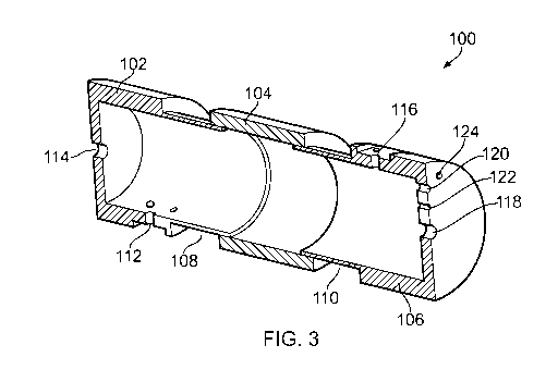
Fig. 3 is a schematic cut-away view of a combined
isolator-diplexer 100 that is an embodiment of the invention.
The combined isolator-diplexer comprising a cylindrical
waveguide isolator along a longitudinal axis of
In Fig. 3 only the electrically conductive elements of
the isolator are depicted.
The cylindrical waveguide isolator of the combined
isolator-diplexer 100 is formed from a pair of end caps 102,
106 separated by collar 104.
The waveguide isolator has an input end formed by an
input end cap 102 that is arranged to receiving an microwave
feed at an input port 112. The input port 112 is arranged on
a circumferential side wall of the input end cap 102. The
input port 112 is adapted to receive a coaxial cable, and
comprising a passageway through the circumferential wall of
the end cap to allow an inner conductor of a connected coaxial
cable (not shown) to extend radially into the cylindrical
space defined by the waveguide isolator. The cylindrical
space may be filled with insulating dielectric material (e.g.
air).
The waveguide isolator has an output end formed by an
output end cap 106 that is connectable to an output line via
an output port 116. The output port 116 is arranged on a
circumferential side wall of the output end cap 106. The
output port 116 is adapted to receive a coaxial cable, and
comprising a passageway through the circumferential wall of
the end cap to allow an inner conductor of a connected coaxial
cable (not shown) to extend radially into the cylindrical
space defined by the waveguide isolator. As discussed in more
detail below, the inner conductor may form part of an RF
diplexer structure for transferring an RF signal into the
coaxial cable that is connected to output port 116. The inner
CA 03070035 2020-01-15
WO 2019/034708
PCT/EP2018/072153
17
conductors of the coaxial cables that protrude into the
cylindrical waveguide cavity are thus insulated from each
other by the dielectric material in the cavity.
In this example, the input port 112 and the output port
116 are on opposing sides of the cylinder formed by the
waveguide. This may be useful to fit with connections to
other components, but it is not essential. In the simulations
discussed below, for example, the input port and output port
are on the same side of the cylinder.
The input end cap 102 and the output end cap 106 are
cylindrical elements having one closed axial end and one open
axial end. The end caps 102, 106 are disposed with there axes
aligned and with their open axial ends facing one another.
The input end cap 102 is configured to be in electrical
communication with an outer conductor of a coaxial cable
connected to the input port 112. The output end cap 106 is
configured to be in electrical communication with an outer
conductor of a coaxial cable connected to the output port 116.
The end caps 102, 106 are physically separated from each other
along the axis of the cylinder. The separation in maintained
by an electrically conductive collar 104 and a pair of
insulating spacers 126, 128 (see Fig. 4) which are
respectively seated in a corresponding circumferential recess
108, 110 formed at the open end of the input end cap 102 and
output end cap 106.
The collar 104 overlies the axial gap between the open
axial ends of the end caps 102, 106 in order to complete the
cylindrical waveguide cavity. In order to insulate the end
caps from each other (and therefore to isolate the outer
conductors of the coaxial cables that are connected thereto),
an insulating layer 127 (see Fig. 4) is disposed around the
outer surfaces of a distal portion of both end caps in order
to provide a dielectric (electrically insulating) barrier in a
circumferential gap between the outer surfaces of the end caps
102, 106 and the inner surface of the collar 104 in a region
where they overlap.
With this arranged, the waveguide isolator comprises two
insulating portions arranged in series along the axis of the
cylinder. A first insulating portion occurs at the overlap
between the input end cap 102 and the collar 104. A second
insulating portion occurs at the overlap between the output
CA 03070035 2020-01-15
WO 2019/034708
PCT/EP2018/072153
18
end cap 106 and the collar 104. With this structure, the
capacitance between the two end caps can be reduced, so that
the capacitance of the structure is less than seen with just
one insulating portion. The reduction in capacitance does not
lead to a meaningful increase in microwave leakage because
most power coupled from the guide is reflected because the
sharp corners at the ends of the cavity create a high
impedance to the passage of the wave.
The insulating layer 127 may be provided by any suitable
material. In one example, the insulating layer 127 may
comprise a plurality (e.g. 2, 3, or more) turns of Kapton0
film. The film material may have a dielectric constant of 3.4
and a dissipation factor of 0.002. The film may have a
thickness of 0.005 mm, and a plurality of turns may be used to
provide the insulating layer with an appropriate thickness.
In other examples, the insulating layer may be a tubular
element, e.g. similar to a washer, that sits between the end
caps 102, 106 and the collar 104. Because the two insulating
gaps are in series, either of which can withstand the required
voltage, the presence of one pinhole in the insulator will not
cause a breakdown of insulation. For this reason the
insulator may be either a coiled (wrapped) dielectric sheet
with multiple layers or a tube, with one layer.
The insulating spacers 126, 128 may each comprise rigid
insulating rings, e.g. made of Delrin0 plastic or
polyvinylchloride (PVC). The spacers may have an axial length
selected to define the correct length for the overlap regions
(each of which can be considered as a separate choke).
As mentioned above, the insulating layer 127 is located
in a circumferential gap between the outer surfaces of the end
caps 102, 106 and the inner surface of the collar 104 in a
region where they overlap. The gap may have a mean diameter
of 41.05 mm and a radial thickness of 0.15 mm. The
capacitance of each gap, which may be partially or completely
filled with the dielectric material of the insulating layer
127, may be around 110 pF. This means that the two gaps in
series provide a capacitance of about 55 pF.
Each of the end caps 102, 106 has a through hole formed
in its closed axial end. The through holes may be arranged
symmetrically with each other with respect to the axis of the
cylinder. In this example, the through holes are on the axis
CA 03070035 2020-01-15
WO 2019/034708
PCT/EP2018/072153
19
of the cylinder. Thus, input end cap 102 has a through hole
114 formed centrally in its closed axial end. The output end
cap 106 has a through holes 118 formed centrally in its closed
axial end. The through holes 114, 118 are arranged to receive
electrically conductive pin or screw elements, which are
selectively and controllably insertable into the cavity to
enable tuning, i.e. to enable optimisation of the insertion
loss and return loss of the combined isolator-diplexer.
In the example shown in Fig. 3, the output end cap
comprises three additional holes 120, 122, 124. These holes
are relating to the diplexer function, which is shown in more
detail in Fig. 5.
Fig. 5 shows a cut-away view of the output end cap 106.
A coaxial cable 142 is connected to the output port 116 using
a suitable connector 138. An inner conductor 140 of the
coaxial cable 142 protrudes into the cavity. The inner
conductor 140 is still surrounded by the dielectric material
141 from the coaxial cable for a portion of the length that it
extends into the cavity.
The diplexer functionality of the device is provided by
introducing a RF connection element 132 perpendicularly
through a hole 120 in the closed end face of the output end
cap 106. The hole 120 is directly in line with the inner
conductor 140 of the output coaxial cable, so that it makes
contact with the inner conductor 140 part of the way down its
length. If the RF connection element 132 is inserted so as to
make contact at the right distance down the centre conductor
then no microwave power is coupled to the RF connection
element 132. This connection affects slightly a match to the
microwave connector but a good match for the microwave energy
can be recovered by making changes to the length of the inner
conductor 140.
The RF connection line 132 is connected to the output end
cap 106 by a connector body 130, which is secured to the
output end cap 106 by pair of screws 134, 136 that are
respectively received in a pair of holes 122, 124 formed in
the closed end face of the output end cap 106. The connector
body 130 comprises a microwave filter 131 for blocking
microwave energy. In this example, the microwave filter 131
is a cylindrical coaxial filter connected to the end of the
output end cap. The cylindrical coaxial filter may be a two
CA 03070035 2020-01-15
WO 2019/034708
PCT/EP2018/072153
section re-entrant coaxial filter, e.g. designed to strongly
reject frequencies at and around 5.8 GHz. The microwave
filter 131 is placed at such a distance from the inside end
wall of the output end cap 106 so that, at microwave
5 frequencies, the RF connection element 132 appears to be
short-circuited to the end wall, to prevent microwave energy
from exiting via the RF connection element 132.
The RF signal (e.g. from input lines 212, 214 as shown in
Fig. 2) is applied between a distal end 133 of the RF
10 connection element 132, and the electrically conductive body
130 of the filter, which in turn is electrically connected to
the outer surface of the output end cap 106. The connection
of the RF signal could be by a standard coaxial connector if
convenient.
15 The RF
connection element 132 extends to touch the inner
conductor 140 of the output coaxial cable (which may take the
form of a microwave connector). The RF connection element 132
may be soldered to the inner conductor 140.
The RF connection element 132 is insulated from the
20 output section and from the other conductive filter parts by
an insulating tube 146 (see Fig. 8), e.g. made from PTFE or
the like. The RF connection element 132 may be a rigid pin
structure. In one example, the RF connection element 132 and
the insulating tube 146 may be constructed by stripping the
outer copper jacket from a short length of semi-rigid coaxial
cable.
Fig. 6 is a cut-away diagram of a simulation model of the
combined isolator-diplexer that is an embodiment of the
invention. Feature already described are given the same
reference number and are not discussed again. For clarity,
with the exception of the three connector pins 132, 140, 154
and two tuning elements 150, 152, Fig. 6 shows only the
dielectric (i.e. electrically insulating) components of the
combined isolator-diplexer. These dielectric components
include air 148 inside the waveguide cavity and air 144 inside
the microwave filter. They also include the dielectric
spacers 126, 128 and insulating layer 127 discussed above. The
simulation was run on the basis that the conductive components
discussed above with reference to Figs. 3 and 5 were also
present.
CA 03070035 2020-01-15
WO 2019/034708
PCT/EP2018/072153
21
There are three ports on the device. Port 1 is the
combined RF/microwave output port. Port 2 is the RF
connection line 132, which introduces RF energy at 400 kHz.
Port 3 is the microwave inlet port, which introduces microwave
energy (e.g. at 5.8 GHz in the preferred example). The
simulation was carried out with both microwave ports (port 1
and port 3) on the same side of the cylinder.
Fig. 7 is a graph showing predicted transmission and
reflection parameters obtained using the simulation model of
the combined isolator-diplexer of Fig. 6, between 4.8 GHz and
6.8 GHz. The inset table on the graph gives the value for
each parameter at 5.8 GHz.
Lines 180, 182 show that the coupling from the input port
and output port to the RF port (S21, S23) is smaller than -60
dB in a range from 5.78 GHz to 5.82 GHz.
Line 186 shows that the match at the input port (S33) is
close to -20 dB at 5.8 GHz.
Line 188 shows that the match at the output port (S11) is
also close to -20 dB at 5.8 GHz.
Line 184 shows that the loss between the input and output
ports (S31, S13) is -0.19 dB at 5.8 GHz.
Fig. 8 is a cut-away section of a simulation model of the
microwave filter 131 mounted at the RF port. The filter has a
cylindrical shape. The RF connection element 132 extends
along an axis of the cylinder. The RF connection element 132
is surrounded by insulating sleeve 146, e.g. made from PTFE.
The filter 131 comprises an electrically conductive body 130
(omitted for clarity in Fig. 8, but shown in Fig. 3) that
defines a pair of axially separated air-filled cavities 144
which act as chokes for inhibiting or prevent passage of
microwave energy. At 5.8 GHz each air-filled cavity are a
quarter-wave long, from the coaxial transmission line to its
closed end. A quarter-wave cavity presents an open circuit in
the outer conductor of the coaxial transmission line that
prevent the 5.8 GHz signal from passing. The spacing of the
cavities is arranged such that each reinforces the effect of
the other. At 400 kHz the filter has no effect, so the RF
signal input is not impeded.
Fig. 9 is a graph showing predicted transmission and
reflection parameters for the microwave filter obtained using
the simulation model of Fig. 8, from 3 GHz to 8.5 GHz.
CA 03070035 2020-01-15
WO 2019/034708
PCT/EP2018/072153
22
Line 160 shows transmission through the filter (S12),
whereas line 162 shows reflection from the filter (S22). The
lines for S21 and Sll are identical to those for S12 and S22.
At 5.8 GHz the predicted insertion loss is very high (-
49.5 dB), and the reflection loss very low (-0.0102 dB). This
performance was with 50 Q loads at each end. In practice,
there may be a higher impedance load at both ends, so that
real performance will differ slightly from the simulation.
For example, the shape and frequency of the dip may vary,
depending on the exact position of both ends, and the
insertion loss may be higher, because of the extra impedance
mismatch.
The following discussion summarises results of
measurements performed on a real example of the combined
isolator-diplexer discussed above.
Measurements were made between port 3 (input) and port 1
(output) as described for Fig. 6, over a frequency range 5.6
GHz to 6 GHz. The measurements of interest were reflection
(S33), transmission (S13), and loss at 5.8 GHz (which is the
preferred frequency of microwave energy).
Coaxial cables were connected to the input port and
output port using microwave connectors. In this example, the
connectors were adapted versions of the Amphenol P/N 172224
component. These connectors were adapted by cutting down the
dielectric such that 1 mm projected into the waveguide cavity
and cutting down the protruding pins (the inner conductors
mentioned above) so that they extending 20 mm from the
connector flange. It is expected that a preferred length of
the pins will be in region of 17.5 mm, so this technique
provides over-long pins that can be trimmed as necessary.
With this set up and by adjusting the screw tuners in
each end cap, a return loss of -34 dB and an insertion loss of
-0.5 dB could be obtained.
The experiment was repeated with a device having the
microwave ports on opposite sides of the waveguide. It was
found that the behaviour was significantly different in this
scenario. This implies that cut-off higher order modes play a
significant part in the coupling, as the fundamental TE01 mode
that can propagate in the waveguide should show no difference
in coupling between connectors on the same side of the
cylinder or on opposite sides. Nevertheless, with the arrange
CA 03070035 2020-01-15
WO 2019/034708
PCT/EP2018/072153
23
of the present invention it is still possible to tune the
combined isolator-diplexer to achieve good performance.