Note: Descriptions are shown in the official language in which they were submitted.
CA 03071505 2020-01-29
WO 2019/025970
PCT/IB2018/055727
COPPER INK
Field
This application relates to printing inks, particularly to printing inks for
printed
electronics.
Backg round
Low price, high conductivity and oxidation resistance are important targets
for
inks in printed electronics. Gold and silver are expensive but stable, i.e.
resistant to
oxidation. Compared to gold and silver, copper is cheaper and has a similar
conductivity;
however, the similar conductivity is often not achieved via printing and the
copper is
prone to oxidation, which reduces conductivity over time. The main types of
copper inks
used are metal nanoparticle-based inks, metal-organic decomposition (MOD)
inks,
copper flake inks and silver-coated copper flake inks.
Nanoparticle-based copper inks are generally expensive but are easily oxidized
and require sintering at very high temperatures and or need laser/flash light
sintering.
Inexpensive versions (e.g. NovacentrixTM) only screen print well on cardboard
and must
be photo-sintered. To prevent oxidation, bimetallic Ag-Cu nanoparticle inks
have been
proposed; but, such inks are still relatively expensive.
MOD inks enable thermal sintering at lower temperature but expensive copper
precursors such as copper formate are typically used. Also, MOD inks are not
typically
viscous, which precludes screen printing. Corrosion caused by strong acid
vapor i.e.
formic acid and poor conductivity due to low metal content are other
limitations often seen
with Cu MOD inks. The main advantage of MOD inks over conventional
flake/nanoparticle
inks is that MOD compounds allow smooth films at low temperature sintering and
produce
high resolution features. However, MOD inks are mixtures of expensive metal
salts, e.g.
copper formate, and organic components, where copper loading in the ink
formulation is
low and can result in lower electrical conductivities of printed traces. Also,
the slow
reactivity of copper traces to atmospheric oxygen (i.e. oxidation) results in
a decrease in
conductivity of traces overtime.
Therefore, there is need for a low cost, high conductivity and oxidation
resistant
screen-printable ink that can be thermally and/or photo-sintered to produce
conducting
traces. Low cost copper inks that are screen-printable on plastic and can be
photo-
sintered or thermally sintered would have immediate commercial value.
1
CA 03071505 2020-01-29
WO 2019/025970
PCT/IB2018/055727
Summary
In one aspect, there is provided a copper-based ink comprising copper
hydroxide
and diethanolamine.
In another aspect, there is provided a method of producing a conductive copper
coating on a substrate, the method comprising: coating a substrate with a
copper-based
ink comprising copper hydroxide and diethanolamine; and, decomposing the ink
on the
substrate to form a conductive copper coating on the substrate.
Advantageously, the ink is low cost and is capable of being formulated for
screen
printing applications. Micron-thick traces of the ink may be screen printed
and thermally
sintered in the presence of up to about 500 ppm of oxygen or photo-sintered in
air to
produce highly conductive copper features. Sintered copper traces produced
from the ink
have improved air stability compared to traces produced from other copper
inks. The
sintered copper traces have good adhesion strength. Copper nanoparticles
and/or silver
salts may be included to further increase conductivity and/or oxidation
resistance of
sintered copper traces, and/or to further enhance screen printability of the
ink. Sintered
copper traces having sheet resistivity of about 20 m0/o/mil or less may be
obtained for 5-
mil wide screen-printed lines with excellent resolution.
Further features will be described or will become apparent in the course of
the
following detailed description. It should be understood that each feature
described herein
20 may be utilized in any combination with any one or more of the other
described features,
and that each feature does not necessarily rely on the presence of another
feature except
where evident to one of skill in the art.
Brief Description of the Drawings
For clearer understanding, preferred embodiments will now be described in
detail
by way of example, with reference to the accompanying drawings, in which:
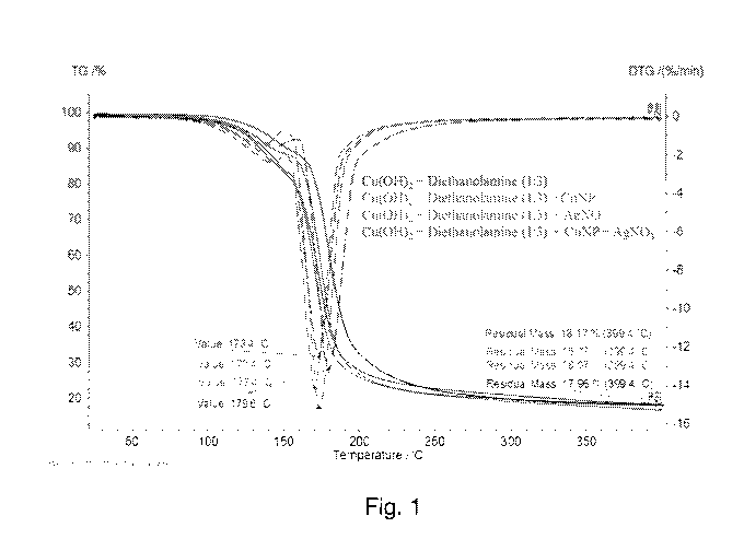
Fig. 1 depicts thermograms of various inks comprising copper hydroxide
monohydrate (Cu(OH)2.1-120) and diethanolamine.
Fig. 2 depicts thermograms of an ink comprising copper hydroxide monohydrate
(Cu(OH)2.1-120) and diethanolamine as a function of storage time.
Fig. 3 depicts a graph of resistance (0) vs. substrate temperature ( C) for
tape
cast traces (5 pm thick, 10 cm long) on a Kapton TM substrate prepared from
various inks
2
CA 03071505 2020-01-29
WO 2019/025970
PCT/IB2018/055727
comprising copper hydroxide monohydrate (Cu(OH)2.1-120) and diethanolamine
thermally
sintered at different temperatures under N2 with 500 ppm 02.
Fig. 4 depicts scanning electron microscopy (SEM) (top) and energy dispersive
spectroscopy (EDS) (bottom) analyses of a copper film (5 pm thick, 1 cm2 area)
on a
KaptonTm substrate prepared using a copper ink comprising Cu(OH)2.1-120 and
diethanolamine (1:3).
Fig. 5 depicts scanning electron microscopy (SEM) (top) and energy dispersive
spectroscopy (EDS) (bottom) analyses of a copper film (5 pm thick, 1 cm2 area)
prepared
on a Kapton TM substrate using a copper ink comprising Cu(OH)2.1-120 and
diethanolamine
(1:3) and copper nanoparticles (10 wt% of the Cu from Cu(OH)2.1-120).
Fig. 6 depicts scanning electron microscopy (SEM) (top) and energy dispersive
spectroscopy (EDS) (bottom) analyses of a copper film (5 pm thick, 1 cm2 area)
on a
KaptonTM substrate prepared using a copper ink comprising Cu(OH)2.1-120 and
diethanolamine (1:3) and silver nitrate (10 wt% of the Cu from Cu(OH)2.1-120).
Fig. 7 depicts scanning electron microscopy (SEM) (top) and energy dispersive
spectroscopy (EDS) (bottom) analyses of a copper film (5 pm thick, 1 cm2 area)
on a
KaptonTM substrate prepared using a copper ink comprising Cu(OH)2.1-120 and
diethanolamine (1:3) and copper nanoparticles (10 wt% of the Cu from Cu(OH)2.1-
120) and
silver nitrate (10 wt% of the Cu from Cu(OH)2.1-120).
Detailed Description
The copper-based ink comprises copper hydroxide and diethanolamine. The
diethanolamine (HN(CH2CH2OH)2) is a readily available organic compound. The
copper
hydroxide (Cu(OH)2) is a readily available inorganic compound and may be
hydrated or
not hydrated. Hydrated copper hydroxide may comprise a monohydrate (Cu(OH)2.1-
120),
which is convenient to use and less expensive than anhydrous copper hydroxide.
In the
ink, copper hydroxide and diethanolamine form a complex. The copper hydroxide
is
preferably present in the ink in an amount that provides about 5 wt% to about
40 wt% of
copper, based on total weight of the ink. The amount of copper, which the
copper
hydroxide provides is more preferably in a range of about 10 wt% to about 30
wt%, based
on total weight of the ink. Preferably, the copper hydroxide and
diethanolamine are in the
ink in a molar ratio of about 1:2.5 to about 1:3.5. More preferably, the molar
ratio of
copper hydroxide to diethanolamine is about 1:3. Such molar ratios are
particularly
advantageous for improving conductivity of conductive copper traces formed
from the ink.
3
CA 03071505 2020-01-29
WO 2019/025970
PCT/IB2018/055727
The ink may also comprise one or more other components useful for the
formulation of inks for specific purposes or for improving electrical,
physical and/or
mechanical properties of conductive traces formed from the ink. In various
embodiments,
the ink may comprise one or more of a filler, a binder, a surface tension
modifier, a
defoaming agent, a thixotropy modifying agent, a solvent, or any mixture
thereof.
The filler, for example another metal-containing compound or a mixture of
other
metal-containing compounds, may be present in the ink to improve conductivity
of
conductive traces formed from the ink. The filler may comprise copper
nanoparticles
(CuNP) or a metal salt. Copper nanoparticles (CuNP) are copper particles
having an
average size along a longest dimension in a range of about 1-1000 nm,
preferably about
1-500 nm, more preferably about 1-100 nm. The copper nanoparticles, may be
flakes,
nanowires, needles, substantially spherical or any other shape. The metal salt
is
preferably a silver or gold salt, more preferably a silver salt. The metal
salt comprises one
or more anions, preferably anions derived from mineral acids. The anions in
the metal
salts are preferably oxide, chloride, bromide, sulfate, carbonate, phosphate,
acetate or
nitrate. Nitrates are particularly preferred. A particularly preferred metal
salt filler is silver
nitrate. The filler is preferably present in the ink in an amount of up to
about 40 wt%,
based on weight of copper from the copper hydroxide in the ink. Preferably,
the amount of
filler is in a range of about 1 wt% to about 40 wt%, or about 5 wt% to about
30 wt%, or
about 10 wt% to about 30 wt%, based on weight of copper from the copper
hydroxide in
the ink.
The binder, for example an organic polymer binder, may be present in the ink
as a
processing aid for particular deposition processes. The organic polymer binder
may be
any suitable polymer, preferably a thermoplastic or elastomeric polymer. Some
non-
limiting examples of binders are cellulosic polymers, polyacrylates,
polystyrenes,
polyolefins, polyvinylpyrrolidone, polypyrrolidone, polyvinyl acetals,
polyesters,
polyimides, polyether imides, polyols, silicones, polyurethanes, epoxy resins,
phenolic
resins, phenol formaldehyde resins, styrene allyl alcohols, polyalkylene
carbonates,
fluoroplastics, fluoroelastomers, thermoplastic elastomers and mixtures
thereof. The
organic polymer binder may be homopolymeric or copolymeric. A particularly
preferred
binder comprises a polyester, polyimide, polyether imide or any mixture
thereof. The
polymeric binder preferably comprises a polyester. Suitable polyesters are
commercially
available or may be manufactured by the condensation of poly alcohols with
poly
carboxylic acid and respectively their anhydrides. Preferred polyesters are
hydroxyl
and/or carboxyl functionalized. The polyester may be linear or branched. Solid
or liquid
4
CA 03071505 2020-01-29
WO 2019/025970
PCT/IB2018/055727
polyesters as well as diverse solution forms may be utilized. In a
particularly preferred
embodiment, the polymeric binder comprises a hydroxyl- and/or carboxyl-
terminated
polyester, for example RokrapolTM 7075. The polymeric binder may be present in
the ink
in any suitable amount. The organic polymer binder may be present in the ink
in any
suitable amount, preferably in a range of about 0.05 wt% to about 10 wt%,
based on total
weight of the ink. More preferably, the amount is in a range of about 0.05 wt%
to about 5
wt%, or about 0.2 wt% to about 2 wt%, or about 0.2 wt% to about 1 wt%. In one
embodiment, the polymeric binder is present in the ink in an amount of about
0.02-0.8
wt%, more preferably about 0.05-0.6 wt%.
The surface tension modifier may be any suitable additive that improves flow
and
leveling properties of the ink. Some non-limiting examples are surfactants
(e.g. cationic or
anionic surfactants), alcohols (e.g. propanol), glycolic acid, lactic acid and
mixtures
thereof. The surface tension modifier may be present in the ink in any
suitable amount,
preferably in a range of about 0.1 wt% to about 5 wt%, based on total weight
of the ink.
More preferably, the amount is in a range of about 0.5 wt% to about 4 wt%, or
about 0.8
wt% to about 3 wt%. In one especially preferred embodiment, the amount is in a
range of
about 1 wt% to about 2.7 wt%.
The defoaming agent may be any suitable anti-foaming additive. Some non-
limiting examples are fluorosilicones, mineral oils, vegetable oils,
polysiloxanes, ester
waxes, fatty alcohols, glycerol, stearates, silicones, polypropylene based
polyethers and
mixtures thereof. Glycerol and polypropylene based polyethers are particularly
preferred.
In the absence of the defoaming agent, some printed traces may tend to retain
air
bubbles following printing, resulting in nonuniform traces. The defoaming
agent may be
present in the ink in any suitable amount, preferably in a range of about
0.0001 wt% to
about 3 wt%, based on total weight of the ink. More preferably, the amount is
in a range
of about 0.005 wt% to about 2 wt%.
The thixotropy modifying agent may be any suitable thixotropy-modifying
additive.
Some non-limiting examples are polyhydroxycarboxylic acid amides,
polyurethanes,
acrylic polymers, latex, polyvinylalcohol, styrene/butadiene, clay, clay
derivatives,
sulfonates, guar, xanthan, cellulose, locust gum, acacia gum, saccharides,
saccharide
derivatives, cassein, collagen, modified castor oils, organosilicones and
mixtures thereof.
The thixotropy modifying agent may be present in the ink in any suitable
amount,
preferably in a range of about 0.05 wt% to about 1 wt%, based on total weight
of the ink.
More preferably, the amount is in a range of about 0.1 wt% to about 0.8 wt%.
In one
5
CA 03071505 2020-01-29
WO 2019/025970
PCT/IB2018/055727
especially preferred embodiment, the amount is in a range of about 0.2 wt% to
about 0.5
wt%.
The solvent may be an aqueous solvent or an organic solvent. In some
instances,
a mixture of one or more organic solvents with an aqueous solvent may be
utilized.
Aqueous solvents include, for example, water and solutions, dispersions or
suspension of
compounds in water. The organic solvent may be aromatic, non-aromatic or a
mixture of
aromatic and non-aromatic solvents. Aromatic solvents include, for example,
benzene,
toluene, ethylbenzene, xylenes, chlorobenzene, benzyl ether, anisole,
benzonitrile,
pyridine, diethylbenzene, propylbenzene, cumene, isobutylbenzene, p-cymene,
tetralin,
trimethylbenzenes (e.g. mesitylene), durene, p-cumene or any mixture thereof.
Non-
aromatic solvents include, for example, terpenes, glycol ethers (e.g.
dipropylene glycol
methyl ether, methylcarbitol, ethylcarbitol, butylcarbitol, triethyleneglycol
and derivatives
thereof), alcohols (e.g. methylcyclohexanols, octanols, heptanols) or any
mixture thereof.
Dipropylene glycol methyl ether is preferred. The solvent may be present in
the ink in any
suitable amount, preferably in a range of about 1 wt% to about 50 wt%, based
on total
weight of the ink. More preferably, the amount is in a range of about 2 wt% to
about 35
wt%, or about 5 wt% to about 25 wt%. The solvent generally makes up the
balance of the
ink.
The ink may be formulated by mixing the components together in a mixer.
Generally, any mixing process is suitable. However, planetary centrifugal
mixing (e.g. in a
ThinkyTm mixer) is particularly useful. Mixing time may have some impact on
the electrical
properties of conductive traces formed from the ink. Properly mixing the ink
ensures good
electrical properties of the conductive traces. The mixing time is preferably
about 25
minutes or less, or about 20 minutes or less, or about 15 minutes or less. The
mixing time
is preferably about 1 minute or more, or about 5 minutes or more.
Prior to decomposition, the ink is deposited on a substrate to coat the
substrate.
Suitable substrates may include, for example polyethylene terephthalate (PET)
(e.g.
MelinexTm), polyolefin (e.g. silica-filled polyolefin (TeslinTm)),
polydimethylsiloxane
(PDMS), polystyrene, acrylonitrile/butadiene/styrene, polycarbonate, polyimide
(e.g.
KaptonTm), polyetherimide (e.g. UltemTm), thermoplastic polyurethane (TPU),
silicone
membranes, printed wiring board substrate (e.g. FR4), wool, silk, cotton,
flax, jute, modal,
bamboo, nylon, polyester, acrylic, aramid, spandex, polylactide, paper, glass,
metal,
dielectric coatings, among others.
6
CA 03071505 2020-01-29
WO 2019/025970
PCT/IB2018/055727
The ink may be coated on the substrate by any suitable method, for example
printing. Printing methods may include, for example, screen printing,
stencilling, inkjet
printing, flexography printing, gravure printing, off-set printing, stamp
printing, airbrushing,
aerosol printing, typesetting, or any other method. It is an advantage of the
process that
an additive method such as screen printing or stenciling are particularly
useful. For
printed electronic devices, the ink may be coated on the substrate as traces.
After coating the substrate with the ink, the ink on the substrate may be
dried and
decomposed to form a copper metal coating on the substrate. Drying and
decomposition
may be accomplished by any suitable technique, where the techniques and
conditions
are guided by the type of substrate and the particular composition of the ink.
For
example, drying and decomposing the ink may be accomplished by heating and/or
photonic sintering.
In one technique, heating the substrate dries and sinters the ink coating to
form
metallic copper. Heating may be performed at a temperature of about 100 C or
higher,
about 140 C or higher, or about 165 C or higher, or about 180 C or higher,
while
producing conductive copper coatings that have good oxidation stability. The
temperature
may be in a range of about 140 C to about 300 C, or about 150 C to about 280
C, or
about 160 C to about 270 C, or about 180 C to about 250 C. Heating is
preferably
performed for a time in a range of about 1-180 minutes, for example 5-120
minutes, or 5-
90 minutes. Heating may be performed in stages to first dry the ink coating
and then
sinter the dried coating. Drying may be performed at any suitable temperature,
for
example at a temperature in a range of about 100 C to about 150 C. Drying may
be
performed for any suitable length of time, for example about 1-180 minutes, or
5-90
minutes, or 10-45 minutes. Sintering is performed at a sufficient balance
between
temperature and time to sinter the ink to form conductive copper coatings.
Drying and/or
sintering may be performed with the substrate under an inert atmosphere (e.g.
nitrogen
and/or argon gas). However, improved air stability of the ink permits
sintering in the
presence of oxygen, for example in an atmosphere comprising up to about 500
ppm of
oxygen. The type of heating apparatus also factors into the temperature and
time
required for drying and sintering.
In another technique, the ink coating may be dried with heat and then
photonically sintered. Drying may be performed at any suitable temperature,
for
example at a temperature in a range of about 100 C to about 150 C. Drying may
be
performed for any suitable length of time, for example about 1-180 minutes, or
5-90
7
CA 03071505 2020-01-29
WO 2019/025970
PCT/IB2018/055727
minutes, or 10-45 minutes. A photonic sintering system may feature a high
intensity
lamp (e.g. a pulsed xenon lamp) that delivers a broadband spectrum of light.
The
lamp may deliver about 5-30 J/cm2 in energy to the traces. Pulse widths are
preferably in a range of about 0.58-1.5 ms. Photonic sintering nay be
performed in air,
or in an inert atmosphere. Laser sintering may be utilized, if desired.
Photonic
sintering is especially suited when polyethylene terephthalate or polyimide
substrates
are used.
A sintered copper coating formed from the ink may have a sheet resistivity of
about 20 mO/o/mil or less, even about 15 mO/o/mil or less, for 5-20 mil wide
screen-
printed lines. Further, line resolution is excellent with changes in line
width after sintering
for 5-20 mil wide screen-printed lines of less than about 17%, or less than
about 10%, or
less than about 5%, or less than about 2.5%. Even when line widths are as low
as about
5 mil, the change in line width after sintering may be less than about 17%,
even less than
about 5%, or even less than about 2.5%. Furthermore, the sintered copper
coatings
formed from the ink may be flexible, being able to pass the ASTM F1683-02 flex
& crease
test without any open circuit breaks (i.e. without open fails). A change in
resistivity (R) of
20% or less is considered to be a pass in the ASTM F1683-02 flex & crease
test. Open
circuit breaks are defined as a total loss in conductivity (i.e. infinite
resistivity).
The substrate having sintered copper coatings thereon may be incorporated into
an electronic device, for example electrical circuits (e.g. printed circuit
boards (PCBs),
conductive bus bars (e.g. for photovoltaic cells), sensors (e.g. touch
sensors, wearable
sensors), antennae (e.g. RFID antennae), thin film transistors, diodes, smart
packaging
(e.g. smart drug packaging), conformable inserts in equipment and/or vehicles,
and
multilayer circuits and MIM devices including low pass filters, frequency
selective
surfaces, transistors and antenna on conformable surfaces that can withstand
high
temperatures.
EXAMPLES:
Example 1 - Preparation of Inks:
Molecular inks were formulated by mixing copper hydroxide monohydrate
(Aldrich)
and diethanolamine (Aldrich) in a 1:3 molar ratio of copper hydroxide to
diethanolamine
and 0 wt% or 0.5 wt% of a carboxyl-terminated polyester binder (RokrapolTM
7075 from
Kramer) to the amount of Cu metal and 0 wt% or 10 wt% CuNP (TEKNATm from
Advanced Material Inc.) to the amount of Cu metal and 0 wt% to 10 wt% AgNO3
(Aldrich)
8
CA 03071505 2020-01-29
WO 2019/025970 PCT/IB2018/055727
to the amount of Cu metal in the total ink. The inks were mixed using a
planetary
centrifugal mixer (e.g. in a Thinky TM mixer) for about 15-30 min at room
temperature.
Example 2 - Thermal Analysis of Inks:
Thermogravimetric analyses of the inks were performed on a Netzsch TG 209 F1
under BOC HP argon (grade 5.3) gas and residual oxygen was trapped with a
Supelco
Big-Supelpure TM oxygen/water trap.
Table 1 and Fig. 1 illustrate the results of thermogravimetric analyses under
argon
of various inks prepared as described in Example 1. All of the inks prepared
comprise
copper hydroxide monohydrate (Cu(OH)2.1-120) and diethanolamine
(HN(CH2CH2OH)2) in
a 1:3 molar ratio of copper hydroxide to diethanolamine. An ink comprising
(Cu(OH)2.1-120) and diethanolamine (HN(CH2CH2OH)2) (11) was analyzed along
with inks
comprising 11 and a fractional amount of other metal fillers (12, 13, 14 and
15). The other
metal fillers were copper nanoparticles (CuNP), silver nitrate (AgNO3) or
mixtures thereof.
The ink compositions are provided below, where wt% is based on weight of Cu
from
Cu(OH)2.1-120:
11 = Cu(OH)2.1-120 + diethanolamine (1:3)
12 = 11 + CuNP (10 wt%)
13 =II + CuNP (20 wt%)
14 = 11 + AgNO3 (10 wt%)
15 =II + CuNP (10 wt%) + AgNO3 (10 wt%)
Table 1 indicates the thermal decomposition temperature for each ink, the
amount
of residue left over at 400 C after thermal decomposition (% based on total
weight of the
ink), the amount of metal in the ink (wt% of Cu or Cu/Ag based on total weight
of the ink),
and whether the ink can be sintered by thermal and photo methods (Y = yes, N =
no).
Table 1
Ink Decomposition Residue (%) wt% metal
Sintering
Temp. ( C) at 400 C in the ink Thermal/Photo
11 179.6 17.96 15.06 Y/Y
12 176.9 17.98 16.56 Y/Y
13 173.4 18.07 18.06 Y/Y
9
CA 03071505 2020-01-29
WO 2019/025970 PCT/IB2018/055727
14 170.4 16.77 16.56 Y/Y
15 173.4 18.17 18.06 Y/Y
The results indicate that all of the inks based on copper hydroxide and
diethanolamine could be thermally and photo-sintered. Further, the
decomposition of 11 is
at about 180 C, and further decreases in the decomposition temperature can be
attained
by adding fractional amounts of CuNP and/or silver (Ag) salt.
Fig. 2 depicts the results of thermogravimetric analyses of the ink 11 under
argon
as a function of storage time. After 1 day of storage at room temperature, the
ink 11 had a
decomposition temperature of 179.1 C, while after 5 days of storage, 11 had a
decomposition temperature of 172.8 C. Further, after 5 days of storage,
thermal
decomposition of 11 resulted in less residual mass (16.75%) at about 400 C
than thermal
decomposition after 1 day (17.96%).
Example 3 - Electrical properties of tape cast traces:
Tape cast traces (5 pm thick, 10 cm long) on a Kapton TM substrate were
prepared
from inks 11, 12, 13, 14 and 15 and thermally sintered at different
temperatures under
nitrogen (N2) with 500 ppm oxygen (02). Resistances of the traces were
measured, and
Table 2 and Fig. 3 provide the results. It is evident that addition of one or
both of CuNP
and Ag salt lowers thermal sintering temperatures to obtain better conducting
traces (i.e.
traces with lower resistance). Resistance of about 100 0 or less are possible
after
sintering at a temperature of about 200 C or higher.
Table 2
Substrate Storage Time Ink 11 Ink 12 Ink 13 Ink 14
Ink 15
Temp. ( C) (Days)
160 C 1h 1
2 2.6 MO
5 2.7 MO 2.4 MO
180 C 1h 1 15 MO 9.6 MO 520 0 13 MO 5.7 MO
2 1000 0 103 0 67 0 530 0 130 0
5 163 0 190 0 100 0 189 0 135 0
200 C 1h 1 163 KO 96 0 65 0 69 0 -- 93 0
220 C 1h 1 62 0 92 0 86 0 40 0 -- 50 0
230 C 1h 1 52 0 60 0 95 0 44 0 -- 34 0
250 C 1h 1 51 0 63 0 63 0 27 0 29 0
110 C 30 min 1 80 0 50 0 24 0 18 0 -- 17 0
250 C 10 min 2 22 0 29 0 16 0 13 0 -- 14 0
5 105 0 48 0 19 0 18 0 13 0
CA 03071505 2020-01-29
WO 2019/025970
PCT/IB2018/055727
Example 4 - Morphological characterization and energy dispersive spectroscopy
(EDS) of
tape cast traces:
Fig. 4 depicts scanning electron microscopy (SEM) (top) and energy dispersive
spectroscopy (EDS) (bottom) analyses of a copper film (5 pm thick, 1 cm2 area)
on a
Kapton TM substrate prepared using ink 11. The SEM images illustrate that the
films have a
porous morphology and the EDS illustrates that the film is formed of pure
copper.
Fig. 5 depicts scanning electron microscopy (SEM) (top) and energy dispersive
spectroscopy (EDS) (bottom) analyses of a copper film (5 pm thick, 1 cm2 area)
prepared
on a Kapton TM substrate using ink 12. The SEM and EDS illustrate that
addition of copper
nanoparticles results in a film that is non-porous and dense, and made of pure
copper.
Fig. 6 depicts scanning electron microscopy (SEM) (top) and energy dispersive
spectroscopy (EDS) (bottom) analyses of a copper film (5 pm thick, 1 cm2 area)
on a
Kapton TM substrate prepared using ink 14. The SEM and EDS illustrate that
addition of a
fractional amount of Ag salt forms silver nanoparticles (bright spots), which
act as
interconnects forming a pure copper/Ag composite film.
Fig. 7 depicts scanning electron microscopy (SEM) (top) and energy dispersive
spectroscopy (EDS) (bottom) analyses of a copper film (5 pm thick, 1 cm2 area)
on a
KaptonTM substrate prepared using ink IS. The SEM and EDS illustrate that
addition of
CuNP forms a dense film, and the addition of a fractional amount of Ag salt
forms silver-
Cu composite nanoparticles (bright spots), which act as interconnects forming
a pure
copper/Ag composite film.
Example 5 - Sintering of screen printed Cu traces:
Inks 16 to 114 were formulated as described in Example 1 comprising
Cu(OH)2.1-120) and diethanolamine (1:3) together with other components as
listed in
Table 3.
Table 3
Ink Binder Filler
16 None None
17 None CuNP (10 wt%)1
18 RokrapolTM 7075 (0.5 wt%)1 CuNP (10 wt%)1
19 None AgNO3 (10 wt%)1
110 RokrapolTM 7075 (0.5 wt%)1 AgNO3 (10 wt%)1
111 RokrapolTM 7075 (0.5 wt%)1 AgN 03 (7.5 wt%)1
11
CA 03071505 2020-01-29
WO 2019/025970
PCT/IB2018/055727
112 RokrapolTM 7075 (0.5 wt%)1 AgN 03 (5 wt%)1
113 RokrapolTM 7075 (0.5 wt%)1 None
114 None CuNP (10 wt%)1 and AgNO3 (10 wt%)1
1 based on weight of the Cu from Cu(OH)2.1-120
Each of the inks was screen printed on a substrate to form traces and then
sintered. The inks were screen printed onto 8.5 in. x 11 in. sheets of
KaptonTM and or
MelinexTm film using a flatbed ATMA screen printer or an American M&M S-912M
small
format screen printer through patterns photoimaged onto kiwocol emulsion (10-
14 pm)
supported on a SS403 stainless steel mesh (Dynamesh, IL). For thermally
processed
samples, the printed traces were sintered at 110 C for 30 min and then 250 C
(substrate
temperature) for 15 min to convert the Cu hydroxide/diethanolamine MOD ink
into
metallic copper. For the samples processed via photonic sintering, the printed
traces
were dried at 140 C for 15 -45 min to remove the solvent and subsequently
processed
under ambient conditions using a PulseForgeTm1300 Novacentrics photonic curing
system.
Example 5-1 - Inks containing no binder or filler (16):
Ink 16 was screen printed on a Kapton TM substrate, dried in a reflow oven at
140 C
for 15 min, and photo-sintered by PulseForge TM sintering at
290V/3000p5/1ps/30ver1ap to
form sintered copper traces on the substrate. Table 4 provides physical and
electrical
properties of the copper traces and Table 5 provides mechanical properties
(flexibility as
per ASTM F1683-02 flex & crease test). As illustrated in Table 4 and Table 5,
ink 16
having no binder or filler provides photo-sintered conducting copper traces
with
reasonable flex properties. Thermal sintering of ink 16 was found to produce
sintered
copper traces that were not conductive.
Table 4
Nominal Linewidth Linewidth # of o 0/o m0/o
linewidth (mil) (pm)
(mil)
5 518 5.24 133 752 0.69 689
10 149 10.49 266 375 0.40 397
15 95 15.28 388 258 0.37 369
20 66 20.57 522 191 0.34 345
Table 5
12
CA 03071505 2020-01-29
WO 2019/025970 PCT/IB2018/055727
Nominal line widths
5 mil 10 mil 15 mil 20 mil
Tensile flex `)/0 change in R 4.4 0.6 3.4 0.9 2.9 0.9
3.2 0.7
open fails 0/5 0/5 0/5 0/5
Compressive flex % change in R 20.6 1.7 17.6 0.6 16.8 5.9 18.7
1.9
open fails 0/5 0/5 0/5 0/5
Tensile crease % change in R 7 2 3.7 2.4 4.4 2.9 3.3 1.4
open fails 0/5 0/5 0/5 0/5
Compressive crease % change in R 5.8 1.8 5 0.9 5.4 0.6 4.7 0.6
open fails 3/5 0/5 0/5 0/5
Example 5-2 - Inks containing CuNP filler but no binder (17):
Ink 17 was screen printed on a Kapton TM substrate and thermally sintered
first at
110 C for 30 min and then at 250 C for 15 min under an atmosphere of N2 with
500 ppm
oxygen. Table 6 and Table 7 provide physical and electrical properties of the
copper
traces produced. As illustrated in Table 6 and Table 7, addition of CuNP to
the ink
enabled the production of screen printed thermally sintered conducting copper
traces.
Table 6
Nominal 0 Linewidth Linewidth # of o 0/o
m0/o
linewidth (mil) (pm)
(mil)
64 12.64 321 312 0.21 205
16 22.44 570 175 0.09 91
9 27.56 700 143 0.06 63
10 Table 7
Nominal Line thickness Thickness Sheet resistivity
Volume resistivity
linewidth (mil) (pm) (mil) (m0/o/mil (p0.cm)
10 1.80 0.071 14.56 36.97
15 3.00 0.12 10.77 27.36
20 4.00 0.16 9.92 25.20
Ink 17 was screen printed on a Kapton TM substrate, dried in a reflow oven at
140 C
for 45 min, and photo-sintered by PulseForge TM sintering at
290V/3000p5/1ps/30ver1ap to
form sintered copper traces on the substrate. Table 8 provides physical and
electrical
15 properties of the copper traces, and Table 9 provides mechanical
properties (flexibility as
13
CA 03071505 2020-01-29
WO 2019/025970 PCT/IB2018/055727
per ASTM F1683-02 flex & crease test). As illustrated by comparing Table 8 to
Table 4,
the addition of CuNP to the ink further increases conductivity of photo-
sintered copper
traces. As illustrated in Table 9, photo-sintered copper traces produced from
the ink 17
passed all mechanical tests. There were no open fails in any of the tests.
Table 8
Nominal Linewidth Linewidth # of o 0/o m0/o
linewidth (mil) (pm)
(mil)
5 215 5.45 138.50 722 0.30 .. 298
101 10.47 266.00 376 0.27 .. 269
75 15.31 389.00 257 0.29 .. 292
48 20.41 518.50 193 0.25 .. 249
Table 9
Nominal line widths
5 mil 10 mil 15 mil __ 20 mil
Tensile flex `)/0 change in R 5.1 0.7 5.2 0.3 4.9
0.4 3.9 0.3
open fails 0/5 0/5 0/5 0/5
Compressive flex % change in R 17.6 1.4 18 1.6 18.8
1.4 18.6 1.6
open fails 0/5 0/5 0/5 0/5
Tensile crease % change in R 3.2 1.1 2.7 0.3 2.8
0.8 2.4 1.1
open fails 0/5 0/5 0/5 0/5
Compressive crease % change in R 4.8 0.2 5.2 0.6 5.3 0.6 5.1 0.6
open fails 0/5 0/5 0/5 0/5
Example 5-3 - Inks containing binder and CuNP filler (18):
10 Ink 18 was
screen printed on a Kapton TM substrate, dried in a reflow oven at 140 C
for 45 min, and photo-sintered by PulseForge TM sintering at
290V/3000p5/1ps/30ver1ap to
form sintered copper traces on the substrate. Table 10 provides physical and
electrical
properties of the copper traces, and Table 11 provides mechanical properties
(flexibility
as per ASTM F1683-02 flex & crease test). As illustrated in Table 10, the
addition of a
15 binder to
the ink still results in sintered copper traces having good conductivity. As
illustrated in Table 11, photo-sintered copper traces produced from the ink 18
passed all
mechanical tests. There were no open fails in any of the tests.
Table 10
14
CA 03071505 2020-01-29
WO 2019/025970 PCT/IB2018/055727
Nominal 0 Linewidth Linewidth # of o 0/o
m0/o
linewidth (mil) (pm)
(mil)
350 5.75 146 685 0.51 511
155 10.59 269 372 0.42 417
95 15.55 395 253 0.38 375
66 20.47 520 192 0.34 343
Table 11
Nominal line widths
5 mil 10 mil 15 mil 20 mil
Tensile flex `)/0 change in R 4.8 0.8 4.9 0.9 4.9
0.9 5 1.4
open fails 0/4 0/4 0/4 0/4
Compressive flex % change in R 14.4 1.3 15 1.2 15.6 1
15.8 1.1
open fails 0/4 0/4 0/4 0/4
Tensile crease % change in R 3.7 0.8 4.1 0.3 4.5 0.7 5.8 1.7
open fails 0/4 0/4 0/4 0/4
Compressive crease % change in R 5.1 0.7 5.1 0.7 5.2 0.7 5.4 0.6
open fails 0/4 0/4 0/4 0/4
Ink 18 was screen printed on a MelinexTM substrate, dried in a reflow oven at
5 140 C for 60 min, and photo-sintered by
PulseForge TM sintering at
230V/6000p5/1ps/30ver1ap to form sintered copper traces on the substrate.
Table 12
provides physical and electrical properties of the copper traces. As
illustrated in Table 12,
conductive copper traces may be formed on a low temperature substrate such as
MelinexTM by photo-sintering screen-printed traces of the ink.
10 Table 12
Nominal 0 Linewidth Linewidth # of o 0/o
m0/o
linewidth (mil) (pm)
(mil)
15 103 15.20 386 259 0.40 398
20 79 20.16 512 195 0.40 404
To illustrate the effect of drying time on conductivity of photo-sintered
copper
traces, ink 18 was screen printed on a Kapton TM substrate, dried in a reflow
oven at 140 C
for different periods of time (10-45 min), and photo-sintered by PulseForge TM
sintering at
15
290V/3000p5/1ps/30ver1ap to form sintered copper traces on the substrate.
Table 13
CA 03071505 2020-01-29
WO 2019/025970 PCT/IB2018/055727
provides the resistance (0) of lines dried for various lengths of time. As
illustrated in
Table 13, longer drying times tend to increase conductivity of the photo-
sintered copper
traces with excellent resolution.
Table 13
Nominal linewidth 10 min 15 min 20 min 30 min 45 min
(mil)
566 0 449 0 350 0
715 0 201 0 214 0 154 0 155 0
441 0 104 0 116 0 92 0 95 0
354 0 76 0 79 0 76 0 66 0
5
Example 5-4 - Inks containing no binder and AgNO3 filler (19):
Ink 19 was screen printed on a Kapton TM substrate and thermally sintered
first at
110 C for 30 min and then at 250 C for 15 min under an atmosphere of N2 with
500 ppm
oxygen. Table 14 and Table 15 provide physical and electrical properties of
the copper-
10 silver composite traces produced, and Table 16 provides mechanical
properties (flexibility
as per ASTM F1683-02 flex & crease test). As illustrated in Table 14, Table 15
and Table
16, the addition of silver salt to the ink enabled the production of screen
printed thermally
sintered conducting copper-silver composite traces without the presence of
binder in the
ink, which passed all mechanical tests without open fails.
15 Table 14
Nominal Linewidth Linewidth # of o 0/o m0/o
linewidth (mil) (pm)
(mil)
5 536 5.31 135.00 741 0.72 724
10 130 10.16 258.00 388 0.34 335
15 68 15.00 381.00 262 0.26 259
20 47 19.29 490.00 204 0.23 230
Table 15
Nominal Line thickness Thickness Sheet resistivity
Volume resistivity
linewidth (mil) (pm) (mil) (m0/o/mil (p0.cm)
5 0.50 0.020 14.24 36.18
10 0.70 0.028 9.24 23.47
15 0.80 0.031 8.16 20.72
16
CA 03071505 2020-01-29
WO 2019/025970
PCT/IB2018/055727
20 0.90 0.035 8.16 20.72
Table 16
Nominal line widths
mil 10 mil 15 mil 20 mil
Tensile flex `)/0 change in R 0.7 0.3 0.5 0.4
open fails 0/3 0/3 0/3 0/3
Compressive flex % change in R 8.0 8.6 7.8 6.9
open fails 0/3 0/3 0/3 0/3
Tensile crease % change in R 11.3 10.6 16 18
open fails 0/3 0/3 0/3 0/3
Compressive crease % change in R 5.36 10.6 5.5 6.3
open fails 0/3 0/3 0/3 0/3
Ink 19 was screen printed on a Kapton TM substrate, dried in a reflow oven at
140 C
5 .. for 15 min, and photo-sintered by PulseForge TM sintering at
300V/3000p5/1ps/30ver1ap to
form sintered copper-silver composite traces on the substrate. Table 17
provides physical
and electrical properties of the copper-silver composite traces, and Table 18
provides
mechanical properties (flexibility as per ASTM F1683-02 flex & crease test).
As illustrated
by comparing Table 17 to Table 4, the addition of silver salt to the ink
further increases
conductivity of photo-sintered traces. As illustrated in Table 18, photo-
sintered copper-
silver composite traces produced from the ink 19 passed all mechanical tests.
Open fails
only occurred at very narrow line widths.
Table 17
Nominal 0 Linewidth Linewidth # of o 0/o
m0/o
linewidth (mil) (pm)
(mil)
3 692 3.35 85 1176 0.59 588
5 207 5.55 141 709 0.29 292
10 67 10.43 265 377 0.18 178
41 15.35 390 256 0.16 160
29 20.47 520 192 0.15 151
15 Table 18
Nominal line widths
17
CA 03071505 2020-01-29
WO 2019/025970 PCT/IB2018/055727
3 mil 5 mil 10 mil 15 mil 20 mil
Tensile flex `)/0 change in R 5.1 0.8 4.1 0.6 3.1 0.9 2.9 1.3
2.8 1
open fails 0/4 0/5 0/5 0/5 0/5
Compressive % change in R 10.7 1.2 11.3 0.9 11.7 0.8 11.3 1.8 12 1.2
flex open fails 0/4 0/5 0/5 0/5 0/5
Tensile crease % change in R 2 0.9 3.2 0.5 4.4 2.1 4.1 1.8
3.2 1.1
open fails 2/4 0/5 0/5 0/5 0/5
Compressive % change in R 2.3 0.7 3.5 0.3 3.6 0.6
3.6 0.6 4 0.7
crease open fails 2/4 0/5 0/5 0/5 0/5
Example 5-5 - Inks containing binder and AgNO3 filler (110):
Ink 110 was screen printed on a KaptonTM substrate, dried in a reflow oven at
140 C for 15 min, and photo-sintered by
PulseForge TM sintering at
300V/3000p5/1ps/30ver1ap to form sintered copper-silver composite traces on
the
substrate. Table 19 provides physical and electrical properties of the copper-
silver
composite traces, and Table 20 provides mechanical properties (flexibility as
per ASTM
F1683-02 flex & crease test). As illustrated in Table 19, the addition of a
binder to the ink
still results in sintered copper-silver composite traces having good
conductivity. As
illustrated in Table 20, photo-sintered copper-silver composite traces
produced from the
ink 110 passed all mechanical tests with a change in R of less than 10% in all
cases and
without open fails.
Table 19
Nominal 0 Linewidth Linewidth # of o 0/o
m0/o
linewidth (mil) (pm)
(mil)
5 286 5.43 138 725 0.39 395
10 84 10.73 272 367 0.23 229
49 15.26 387 258 0.19 190
36 19.88 505 198 0.18 182
15 Table 20
Nominal line widths
5 mil 10 mil 15 mil 20 mil
Tensile flex % change in R 1.5 0.3 1.7 0.4 1.7 0.6
1.8 1.2
open fails 0/5 0/5 0/5 0/5
Compressive flex % change in R 5.1 1 5.1 1 5.4 1 5.5 1
open fails 0/5 0/5 0/5 0/5
18
CA 03071505 2020-01-29
WO 2019/025970 PCT/IB2018/055727
Tensile crease `)/0 change in R 1.7 0.3 1.8 0.7 1.9 0.3
1.9 0.4
open fails 0/5 0/5 0/5 0/5
Compressive crease % change in R 1.7 0.4 1 .1 1.8 1 0.8
1.7 0.7
open fails 0/5 0/5 0/5 0/5
Ink 110 was screen printed on a MelinexTM substrate, dried in a reflow oven at
140 C for 60 min, and photo-sintered by
PulseForge TM sintering at
300V/1500ps/1ps/30ver1ap_2X to form sintered copper-silver composite traces on
the
substrate. Table 21 provides physical and electrical properties of the copper-
silver
composite traces. As illustrated in Table 21, conductive copper-silver
composite traces
may be formed on a low temperature substrate such as MelinexTM by photo-
sintering
screen-printed traces of the ink.
Table 21
Nominal Linewidth Linewidth # of o 0/o
m0/o
linewidth (mil) (pm)
(mil)
316 10.35 263 380 0.83 831
230 12.68 322 311 0.74 741
To illustrate the effect of drying time on conductivity of photo-sintered
copper-
silver composite traces, ink 110 was screen printed on a Kapton TM substrate,
dried in a
reflow oven at 140 C for different periods of time (10-60 min), and photo-
sintered by
PulseForgeTM sintering at 300V/3000p5/1ps/30ver1ap to form sintered copper-
silver
composite traces on the substrate. Table 22 provides the resistance (0) of
lines dried for
various lengths of time. As illustrated in Table 22, drying times from about
15 minutes to
minutes tend to increase conductivity of the photo-sintered copper-silver
composite
traces with excellent resolution.
Table 22
Nominal linewidth 10 min 15 min 20 min 30 min 60 min
(mil)
5 536 0 286 0 325 0 419 0 1300 0
10 132 0 84 0 89 0 122 0 188 0
15 77 0 49 0 49 0 70 0 110 0
20 58 0 36 0 36 0 49 0 86 0
19
CA 03071505 2020-01-29
WO 2019/025970 PCT/IB2018/055727
To illustrate the effect of the amount of AgNO3 filler on conductivity of
photo-
sintered copper-silver composite traces, inks 110, 111, 112 and 113 were
screen printed on
a KaptonTM substrate, dried at 140 C for 15 min), and photo-sintered by
PulseForgeTM
sintering at 300V/3000ps/1ps/3overlap to form sintered copper-silver composite
traces on
the substrate. Table 23 provides resistances (0) of the copper-silver
composite traces. As
illustrated in Table 23, there is a systematic increase in the conductivity of
copper-silver
composite traces with the addition of silver salt.
Table 23
Nominal linewidth Ink 113 Ink 112 Ink Ill Ink 110
(mil) (0% Ag NO3) (5% Ag NO3) (7.5% Ag NO3) (10% Ag NO3)
5 844 0 319 0 298 0 286 0
255 0 124 0 101 0 84 0
137 0 66 0 54 0 49 0
87 0 50 0 39 0 36 0
10 Example 5-6 - Inks containing binder, CuNP filler and AgNO3 filler
(114):
Ink 114 was screen printed on a Kapton TM substrate and thermally sintered
first at
110 C for 30 min and then at 250 C for 15 min under an atmosphere of N2 with
500 ppm
oxygen. Table 24 and Table 25 provide physical and electrical properties of
the copper-
silver composite traces produced, and Table 26 provides mechanical properties
(flexibility
15 as per ASTM F1683-02 flex & crease test). As illustrated in Table 24,
Table 25 and Table
26, the addition of both copper nanoparticles and silver salt to the ink
enabled the
production of screen printed thermally sintered conducting copper-silver
composite traces
without the presence of binder in the ink, which passed all mechanical tests
without open
fails.
20 Table 24
Nominal Linewidth Linewidth # of o 0/o
m0/o
linewidth (mil) (pm)
(mil)
5 600 6.30 160.00 625 0.96 960
10 191 12.60 320.00 313 0.61 611
15 107 16.65 423.00 236 0.45 453
20 77 22.05 560.00 179 0.43 431
Table 25
CA 03071505 2020-01-29
WO 2019/025970 PCT/IB2018/055727
Nominal Line thickness Thickness Sheet
resistivity Volume resistivity
linewidth (mil) (pm) (mil) (mO/o/mil (p0.cm)
0.45 0.018 17.01 43.20
0.70 0.028 16.84 42.78
0.80 0.031 14.26 36.20
0.90 0.035 15.28 38.80
Table 26
Nominal line widths
5 mil 10 mil 15 mil 20
mil
Tensile flex `)/0 change in R 0.70 0.92 0.47 0.60
open fails 0/3 0/3 0/3 0/3
Compressive flex % change in R 10.5 9.7 9.1 5.9
open fails 0/3 0/3 0/3 0/3
Tensile crease % change in R 9.1 10.2 13.9 13.2
open fails 0/3 0/3 0/3 0/3
Compressive crease % change in R 9.3 9.6 9.4 8.2
open fails 0/3 0/3 0/3 0/3
Example 6 - Comparison to inks formulated with different copper precursors and
5 alkanolamines:
To assess the effect of replacing copper hydroxide and diethanolamine with
other
copper precursor molecules and other alkanolamines, various inks were
formulated in the
same manner as ink 11 except that one or both of the copper hydroxide and
diethanolamine were replaced as indicated in Table 27. The inks were deposited
on
10 Kapton TM
substrates and samples were thermally sintered. Table 27 provides the results.
As illustrated in Table 27, only ink 11 provided conductive copper traces when
thermally
sintered. All other inks resulted oxidized, non-conducting black traces. Ink
11 also
provides conducting traces when photo-sintered, as described above.
Table 27
Ink Copper Alkanolamine Thermal sintering
precursor
11 Cu(OH)2.1-120 Diethanolamine Conducting
Cl Cu(OH)2.1-120 Monoethanolamine
Oxidation, non-conducting
C2 Cu(OH)2.1-120 Triethanolamine
Oxidation, non-conducting
C3 Cu(OH)2.1-120 N-Butyldiethanol amine
Oxidation, non-conducting
C4 Cu(OH)2.1-120 3-
(Dimethylamino)-1,2-propanediol Oxidation, non-conducting
21
CA 03071505 2020-01-29
WO 2019/025970
PCT/IB2018/055727
C5 Cu(OH)2.1-120 3-(Diethylamino)-1,2-propanediol
Oxidation, non-conducting
C6 Cu(OH)2.1-120 2-Amino-1-butanol
Oxidation, non-conducting
C7 Cu(OH)2.1-120 Amino-2-propanol
Oxidation, non-conducting
C8 Cu(OH)2.1-120 2-Diethylamino ethanol
Oxidation, non-conducting
C9 Cu(OH)2.1-120 1-Dimethylamino-2-propanol
Oxidation, non-conducting
C10 Cu(OH)2.1-120 2-Amino-2-methyl-1-propanol
Oxidation, non-conducting
C11 Cu(OH)2.1-120 3-Diemthylamino-1-propanol
Oxidation, non-conducting
C12 Cu(OH)2.1-120 2-(Diisopropylamino)-ethanol
Oxidation, non-conducting
C13 Cu(OH)2.1-120 Tri-isopropanolamine
Oxidation, non-conducting
C14 CuCl2 Diethanolamine
Oxidation, non-conducting
C15 CuCl2 Monoethanolamine
Oxidation, non-conducting
C16 CuCl2 3-(Diethylamino)-1,2-propanediol
Oxidation, non-conducting
C17 CuCl2 2-Amino-1-butanol
Oxidation, non-conducting
C18 CuSO4 Diethanolamine
Oxidation, non-conducting
C19 CuSO4 Monoethanolamine
Oxidation, non-conducting
C20 CuSO4 3-(Diethylamino)-1,2-propanediol
Oxidation, non-conducting
C21 CuSO4 2-Amino-1-butanol
Oxidation, non-conducting
C22 Cu oxalate Diethanolamine
Oxidation, non-conducting
hemihydrate
C23 Cu oxalate Monoethanolamine
Oxidation, non-conducting
hemihydrate
C24 Cu oxalate 3-(Diethylamino)-1,2-propanediol
Oxidation, non-conducting
hemihydrate
C25 Cu oxalate 2-Amino-1-butanol
Oxidation, non-conducting
hemihydrate
Example 7¨ Cost comparison of inks
To illustrate the cost efficiency of copper inks, the costs of copper
hydroxide/diethanolamine inks of the present invention were compared to the
cost of the
ink if the copper hydroxide is replaced by other popular MOD compounds, namely
copper
formate tetrahydrate and silver neodecanoate. Table 28 illustrates a cost
comparison (in
Canadian dollars) when the ink comprises a copper nanoparticle (CuNP) filler
and Table
29 illustrates a cost comparison (in Canadian dollars) when the ink comprises
a silver
nitrate (AgNO3) filler. The lowest catalogue price for the copper salts was
from Alfa and
the lowest catalogue price for silver neodecanoate was from Gelest Inc.
Further, 1 g of
copper hydroxide has 65.12% Cu, 1 g of copper formate has 28% Cu, and 1g of
silver
neodecanoate has 38.64% Ag; therefore, the per gram metal precursor price was
scaled
to a metal content of 65%.
As illustrated in Table 28 an ink based on copper hydroxide and filled with
copper
nanoparticles is more than about 8x less expensive than a similar ink based on
copper
formate and more than about 42x less expensive than a similar ink based on
silver
neodecanoate. Even when a silver salt is used as a filler, as illustrated in
Table 29, the
22
CA 03071505 2020-01-29
WO 2019/025970
PCT/IB2018/055727
ink based on copper hydroxide is more than 4x less expensive than the ink
based on
copper formate and more than 21x less expensive than the ink based on silver
neodecanoate.
Table 28
Lowest Ratio Cost Cost Cost
catalogue price Copper Copper formate Silver
hydroxide ink ink neodecanoate ink
Metal precursor 1 g $0.075 $1.64 $8.75
Diethanolamine 3 g $0.084 $0.084 $0.084
CuNP 0.1 g $0.05 $0.05 $0.05
Total for ink 4.1 g $0.209 $1.774 $8.88
Per gram for ink 1 g $0.051 $0.43 $2.16
Table 29
Lowest Ratio Cost Cost Cost
catalogue price Copper Copper formate Silver
hydroxide ink ink neodecanoate ink
Metal precursor 1 g $0.075 $1.64 $8.75
Diethanolamine 3 g $0.084 $0.084 $0.084
AgNO3 0.1 g $0.26 $0.26 $0.26
Total for ink 4.1 g $0.419 $1.984 $9.90
Per gram for ink 1 g $0.102 $0.483 $2.21
The novel features will become apparent to those of skill in the art upon
examination of the description. It should be understood, however, that the
scope of the
claims should not be limited by the embodiments, but should be given the
broadest
interpretation consistent with the wording of the claims and the specification
as a whole.
23