Note: Descriptions are shown in the official language in which they were submitted.
CA 03071730 2020-01-31
WO 2019/025230 PCT/EP2018/069981
1
A light emitting device, comprising light emitting units being arranged in a
plane filling
pattern
FIELD OF THE INVENTION
In the first place, the invention relates to a light emitting device,
comprising
light emitting units being arranged in a plane filling pattern for covering at
least a substantial
portion of a surface, wherein individual light emitting units comprise an
internal electrical
circuit and at least two connection areas providing electrical access to the
internal electrical
circuit from outside of the light emitting units, and wherein the light
emitting units are
electrically interconnected through the connection areas thereof.
In the second place, the invention relates to a set of light emitting units
designed to be arranged in a plane filling pattern for covering at least a
substantial portion of
a surface and to thereby constitute the light emitting device as mentioned,
wherein individual
light emitting units of the set comprise an internal electrical circuit and at
least two
connection areas providing electrical access to the internal electrical
circuit from outside of
the light emitting units, and wherein the connection areas of the light
emitting units are
designed to enable an arrangement of the light emitting units in which the
light emitting units
are electrically interconnected through the connection areas thereof.
In the third place, the invention relates to an assembly of a marine object
and
the light emitting device as mentioned, the marine object comprising at least
one surface that
is intended to be at least partially submersed in a fouling liquid containing
biofouling
organisms during at least a part of the lifetime of the marine object, and the
light emitting
device being arranged on the at least one surface.
In the fourth place, the invention relates to a method for assembling a light
emitting device, comprising the steps of providing light emitting units
comprising an internal
electrical circuit and at least two connection areas providing electrical
access to the internal
electrical circuit from outside of the light emitting units, arranging the
light emitting units in
a plane filling pattern for covering at least a substantial portion of a
surface, and electrically
interconnecting the light emitting units through the connection areas thereof.
CA 03071730 2020-01-31
WO 2019/025230
PCT/EP2018/069981
2
BACKGROUND OF THE INVENTION
In general, the invention is in the field of realizing a light emission effect
by
using a number of light emitting units arranged in a plane filling pattern.
One possible
specific application of the invention is an application for the purpose of
anti-fouling of
surfaces. The background of the invention will now be explained in the context
of that
specific application, which should not be understood so as to imply that the
invention is
limited to that application.
Fouling of surfaces that are exposed to water, during at least a part of their
lifetime, is a well-known phenomenon that causes substantial problems in many
fields. For
example, in the field of shipping, biofouling on the hull of ships is known to
cause a severe
increase in drag of the ships, and thus increased fuel consumption of the
ships. In this respect,
it is estimated that an increase of up to 40% in fuel consumption can be
attributed to
biofouling.
In general, biofouling is the accumulation of microorganisms, plants, algae,
small animals and the like on surfaces. According to some estimates, over
1,800 species
comprising over 4,000 organisms are responsible for biofouling. Hence,
biofouling is caused
by a wide variety of organisms, and involves much more than an attachment of
barnacles and
seaweeds to surfaces. Biofouling is divided into micro fouling which includes
biofilm
formation and bacterial adhesion, and macro fouling which includes the
attachment of larger
organisms. Due to the distinct chemistry and biology that determine what
prevents them from
settling, organisms are also classified as being hard or soft. Hard fouling
organisms include
calcareous organisms such as barnacles, encrusting bryozoans, mollusks,
polychaetes and
other tube worms, and zebra mussels. Soft fouling organisms include non-
calcareous
organisms such as seaweed, hydroids, algae and biofilm "slime". Together,
these organisms
form a fouling community.
Biofouling can cause machinery to stop working and water inlets to get
clogged, to mention only two other negative consequences than the above-
mentioned
increase of drag of ships. In any case, the topic of anti-biofouling, i.e. the
process of
removing and/or preventing biofouling, is well-known.
WO 2014/188347 Al discloses a method of anti-fouling of a surface while
said surface is at least partially submersed in a liquid environment, in
particular an aqueous
or oily environment. The method involves providing an anti-fouling light and
providing an
optical medium in close proximity to such a protected surface, the optical
medium having a
substantially planar emission surface. At least part of the light is
distributed through the
CA 03071730 2020-01-31
WO 2019/025230 PCT/EP2018/069981
3
optical medium in a direction substantially parallel to the protected surface,
and the anti-
fouling light is emitted from the emission surface of the optical medium, in a
direction away
from the protected surface. The anti-fouling light may be ultraviolet light,
and the optical
medium may comprise ultraviolet transparent silicone, i.e. silicone that is
substantially
transparent to ultraviolet light, and/or ultraviolet grade fused silica, in
particular quartz.
By applying the method known from WO 2014/188347 Al, it is possible to
cover a protected surface to be kept clean from biofouling, at least to a
significant extent,
with a layer that emits germicidal light. The protected surface can be the
hull of a ship, as
mentioned earlier, but the method is equally applicable to other types of
surface.
WO 2014/188347 Al further discloses a lighting module that is suitable to be
used for putting the above-mentioned method to practice. Thus, the lighting
module
comprises at least one light source for generating anti-fouling light and an
optical medium for
distributing the anti-fouling light from the light source. The at least one
light source and/or
the optical medium may be at least partially arranged in, on and/or near the
protected surface
.. so as to emit the anti-fouling light in a direction away from the protected
surface.
The lighting module known from WO 2014/188347 Al may be provided as a
foil that is suitable for application to the protected surface. The foil may
be substantially size-
limited in two orthogonal directions perpendicular to a thickness direction of
the foil, so as to
provide a tile-shaped anti-fouling unit; in another embodiment, the foil is
substantially size-
limited in only one direction perpendicular to the thickness direction of the
foil, so as to
provide an elongated strip of anti-fouling foil.
The concept of having tile-shaped anti-fouling units is particularly
interesting
when it comes to subjecting large surfaces to an anti-fouling action, which
may be surfaces
being as large as up to more than 10,000 m2. Anti-fouling units can be of any
suitable shape
.. and size. For example, square units may be used and arranged in a regular
pattern on a ship's
hull for forming an anti-fouling light emitting device on the hull, wherein
each unit may be
dimensioned so as to cover about 1 m2 of the hull. For the purpose of proper
operation of the
anti-fouling light emitting device, the units need to be electrically
interconnected, and the
whole of the units needs to be connected to an electric power source as well.
However, the
costs of the light emitting device are directly related to the number of
connections to the
units. Further, in some cases, connections to the units are quite vulnerable
to water ingress,
and thus electrical shorts may occur when at least a part of the anti-fouling
light emitting
device is actually under the waterline. It would be easy to reduce the risk of
malfunctions,
namely by limiting the amount of connections, if it was not for the fact that
it is also
CA 03071730 2020-01-31
WO 2019/025230 PCT/EP2018/069981
4
important for the device to have a certain level of electrical redundancy. For
the sake of
completeness, it is noted that the term "redundancy" as used in the present
text should be
understood so as to relate to alternative paths for the power in case of
failure of a unit or a
connection between units. The more alternative paths are available, the less
likely it is for the
units to be cut off from a power source in case of damage to the light
emitting device, and the
higher the electrical redundancy. In fact, electrical redundancy of a light
emitting device is
high if a layout is chosen such that functioning of the device is not affected
by damage to the
layout, even if damage occurs at many different positions, and if
malfunctioning of one or
more units does not cause other units to be inoperative as well, whereas
electrical redundancy
of a light emitting device is low if a layout is chosen such that functioning
of the device is
affected by damage to the layout at only one or a few positions and/or by
malfunctioning of
only one or a few units.
In a light emitting device, all of the light emitting units that are included
in the
device need to be connected to the electric power source somehow. For obvious
reasons, it is
desirable to only have one electric power source for powering a large number
of light
emitting units. In order to prevent a situation in which as many electric
wires or other
electrically conductive elements as light emitting units would be needed for
electrically
interconnecting each of the light emitting units and the power source, it is
practical to daisy
chain light emitting units, which implies that light emitting units are
connected in a
successive arrangement, wherein one end of the daisy chain is connected to the
power source.
However, a long series of daisy chained light emitting units has no redundancy
and is quite
vulnerable to damage of a single connection between light emitting units
and/or of a light
emitting unit. When one connection or light emitting unit fails, all light
emitting units down
the line of that connection or light emitting unit cannot be powered.
Introducing redundancy
would require using more than a minimum of two electrical connections per
light emitting
unit so as to have additional connections allowing for alternative routes of
the electric power.
It is an object of the invention to provide a practical solution to the
situation of the conflicting
requirements of limiting the number of connections on the one hand and having
a sufficient
level of electrical redundancy on the other hand.
WO 2009/069076 A2 relates to an electronic tile that implements variable
parameters such as color and/or brightness and/or temperature. The tile is
intended to be
inserted in a system of several identical tiles for covering a surface, which
system comprises
a special tile for controlling the various parameters, so that a person can
change the
CA 03071730 2020-01-31
WO 2019/025230 PCT/EP2018/069981
appearance of the system of tiles according to desire. At least one tile of
the system is
connected to the electrical supply.
The tile known from WO 2009/069076 A2 may particularly comprise one or
more LEDs and is designed to implement the functionalities thereof without any
wiring.
5 Assuming a square periphery of the tile, in which case the tile has four
corners, it may be so
that the tile is recessed at the position of the corners, and that electrical
contacts of the tile are
positioned at that very position. Connecting one tile to another involves
using a separate
piece having electrical contacts as well, which is then made to contact both a
corner of the
one tile and a corner of the other tile.
WO 2012/041456 Al relates to a lighting system for decorating a wall, a
ceiling or a floor. The lighting system comprises a plurality of square
decorative tiles, a
plurality of contact elements being arranged on the border region of each of
the tiles,
including the corners of each of the tiles. The decorative tiles are
electrically connected to
each other through their contact elements, wherein physical connections
between the contact
elements of respective tiles are realized through contact plates which are
placed at
appropriate positions in the lighting system.
SUMMARY OF THE INVENTION
According to a first aspect of the invention, a light emitting device is
provided,
that comprises light emitting units being arranged in a plane filling pattern
for covering at
least a substantial portion of a surface, wherein individual light emitting
units comprise an
internal electrical circuit and at least two connection areas providing
electrical access to the
internal electrical circuit from outside of the light emitting units, wherein
the light emitting
units are electrically interconnected through the connection areas thereof,
wherein at least
one of the connection areas of individual light emitting units is electrically
connected
simultaneously to respective connection areas of at least two other light
emitting units, and
wherein the light emitting units overlap at the positions of at least portions
of the connection
areas where individual light emitting units are electrically connected
simultaneously to
respective connection areas of at least two other light emitting units.
As explained in the foregoing, connecting an electrically conductive element
to each light emitting unit for enabling each light emitting unit to be
directly connected to an
electric power source would yield a high level of electrical redundancy, but
would result in
an unacceptable amount of electrically conductive elements and an associated
risk of
failures/electrical shorts. Daisy chaining light emitting units does not offer
a practical
CA 03071730 2020-01-31
WO 2019/025230 PCT/EP2018/069981
6
solution to the problem, as doing so involves a risk of a number of light
emitting units being
rendered inoperable when only one connection in a chain of light emitting
units fails. Making
a structure of connections in order to have each light emitting unit in a
daisy chain of light
emitting units and to also allow for an alternative power route through an
adjacent daisy
chain would increase the level of electrical redundancy without a need for
providing a way of
enabling each light emitting unit to be directly connected to an electric
power source, but
would involve a large number of electrical connections between the light
emitting units.
The invention proposes another approach and relies on making electrical
connections between at least three light emitting units at one position,
namely a position
where respective connection areas of the at least three light emitting units
come together, at
least in a functional sense, so that the connection areas can be
interconnected. In that way, it
appears to be possible to reduce the number of physical connections between
light emitting
units while maintaining an acceptable level of electrical redundancy. In
particular, it appears
that by making connections between at least three light emitting units at one
position, which
will hereinafter be referred to as combined connections, an effective
structure is obtained in
which individual light emitting units are at a position for receiving power
through alternative
connection routes, so that failure of a light emitting unit or a connection to
a light emitting
unit does not affect the functioning of the other light emitting units, and in
which the number
of physical connections that is needed for realizing the structure is reduced.
For example, it is possible for the light emitting device to comprise combined
connections of four light emitting units. In such a case, compared to a
conventional situation
in which each connection is only between two light emitting units, it is
achieved that the total
number of connections between light emitting units in the light emitting
device can be
reduced by roughly 50% while still having the same level of electrical
redundancy. Further,
in such a case, it may be practical for the light emitting units to be
arranged in a regular
pattern of rows and columns of light emitting units, and for the combined
connections of four
light emitting units to be located at positions where four light emitting
units meet, i.e.
positions both between two rows and between two columns, which will
hereinafter be
referred to as nodal positions. In such a pattern, in order to have the
sufficient level of
electrical redundancy as desired, it is not necessary for all nodal positions
between the light
emitting units as present in the pattern to be positions where four light
emitting units are
interconnected. Instead, it may suffice if combined connections are provided
at every other
nodal position, both in the direction of the rows and the direction of the
columns of the
pattern.
CA 03071730 2020-01-31
WO 2019/025230 PCT/EP2018/069981
7
Within the framework of the invention, the actual physical positioning of at
least three light emitting units as may be involved in a combined connection
can be chosen
freely, provided that the at least three light emitting units overlap at the
positions of at least
portions of the connection areas where the at least three light emitting units
are electrically
connected simultaneously to respective connection areas of the at least two
other light
emitting units. Those light emitting units may be arranged in the plane
filling pattern so as to
mainly be adjacent light emitting units in a physical sense, but that is not
essential. The fact is
that the concept of interconnecting respective connection areas of at least
three light emitting
units is not limited to any physical way of establishing electrical
connections. All light
emitting units of the light emitting device may be of a single type, i.e. may
be identical, but it
is also possible that two or even more different types of light emitting units
are applied in the
light emitting device. In this respect, it may especially be practical if
light emitting units of at
least two different shapes are applied in the light emitting device.
For the sake of completeness, it is noted that the term "a plane filling
pattern"
.. should be understood in a practical sense, i.e. so as to cover various
options which would
normally be denoted by a skilled person by means of the term, including an
option according
to which light emitting units are arranged in a closely adjoining fashion,
with practically no
space between the light emitting units, and an option according to which light
emitting units
are arranged beside each other with only a narrow space between them. In
general, the term is
applicable to both a pattern in which the light emitting units are arranged so
as to form a
continuous cover of a surface and a pattern in which the light emitting units
are arranged so
as to form a cover of a surface that is provided with interruptions, the
interruptions being no
more than small areas between the light emitting units, wherein the larger
part of the total
area of the pattern is occupied by the light emitting units. In any case, it
may particularly be
so that mutual distances between light emitting units are significantly
smaller than general
dimensions of the light emitting units. In general, the light emitting units
may be provided as
tiles, panels or the like suitable for arrangement on a surface to be covered.
In practical situations, it may be so that the light emitting device comprises
a
number of light emitting units that cannot be typified as being light emitting
units of which at
least one of the connection areas is involved in a combined connection,
especially light
emitting units having a corner position or a side position in a pattern of
light emitting units,
which does not alter the fact that the invention is realized in the other
light emitting units,
which will normally be the majority of the total number of light emitting
units of a light
emitting device.
CA 03071730 2020-01-31
WO 2019/025230 PCT/EP2018/069981
8
As mentioned in the foregoing, the light emitting units comprise at least two
connection areas for providing electrical access to the internal electrical
circuit of the light
emitting units from outside of the light emitting units. Within the framework
of the invention,
it may be so that at least two of the connection areas of individual light
emitting units are
electrically connected simultaneously to respective connection areas of at
least two other
light emitting units, i.e. are involved in a combined connection. In such a
case, considering
the option as mentioned at the level of an arbitrary light emitting unit from
the pattern, it is
most practical if one of the at least two of the connection areas of the light
emitting unit is
involved in a combined connection between the light emitting unit and a first
set of at least
two other light emitting units, and another of the at least two of the
connection areas of the
light emitting unit is involved in a combined connection between the light
emitting unit and a
second set of at least two other light emitting units, different from the
first set of at least two
other light emitting units, so that the light emitting unit is connected to as
many other light
emitting units as possible.
It is to be noted that the invention also covers an option according to which
no
more than two of the connection areas of individual light emitting units are
electrically
connected simultaneously to respective connection areas of at least two other
light emitting
units. Further, it may be practical if (exactly) two of the connection areas
of individual light
emitting units are electrically connected simultaneously to respective
connection areas of at
least two other light emitting units.
Alternatively or additionally, it may be so that at least one other of the
connection areas of the light emitting units is electrically connected to a
connection area of
only one other light emitting unit. In other words, the invention is already
put to practice if
not all of the connection areas of the light emitting units are involved in a
combined
connection, wherein it is possible for the light emitting device to comprise
both combined
connections and conventional, single connections between light emitting units.
According to the invention, the light emitting units are arranged so as to
overlap at the positions of at least portions of the connection areas where
individual light
emitting units are electrically connected simultaneously to respective
connection areas of at
least two other light emitting units, i.e. at the positions of at least the
connection areas that are
involved in combined connections between light emitting units. For example, it
may be so
that individual light emitting units comprise at least one recessed portion,
wherein at least
one connection area of the light emitting units comprises at least one
electrically conductive
connection member that is arranged on the light emitting units at the position
of their at least
CA 03071730 2020-01-31
WO 2019/025230 PCT/EP2018/069981
9
one recessed portion, and that is in electrical connection with the internal
electrical circuit of
the light emitting units, and wherein the light emitting units partially
overlap at the positions
of their recessed portions. The electrically conductive connection member of
the at least one
connection area may be realized in the form of an electrically conductive
strip extending on
an external surface portion of the light emitting unit, for example.
Letting the light emitting units partially overlap at the positions of
recessed
portions of the light emitting units allows for having an arrangement in which
the light
emitting units are located at a single level, especially when a height of the
light emitting units
at the positions of the recessed portions is chosen to be no more than half of
a general height
of the light emitting units, and the light emitting units are alternately
arranged with the
recessed portion up and the recessed portion down so that the recessed
portions of the light
emitting units can face each other whereas, apart from the recessed portions,
the light
emitting units are arranged beside each other.
As is the case in conventional situations, the light emitting device may
comprise electrically conductive wiring for establishing the necessary
electrical connections
between the light emitting units. For example, wire assemblies of electrically
interconnected
wires may be provided for establishing combined connections between at least
three light
emitting units, wherein each of the at least three light emitting units is
connected to a
respective wire end of the wire assemblies. However, it may be more practical
if another type
of electrically conductive element is used, such as an electrically conductive
bump or track.
In any case, the connection areas of the light emitting units may comprise an
electrically
conductive strip or the like, as already suggested in the foregoing, in which
case something
like an electric wire, or an electrically conductive bump or track may be
provided so as to
interconnect the electrically conductive strips or the like. In general, any
connector known for
.. making electrically conductive connections at a relatively small scale will
do. Alternatively,
the electrically conductive strips or the like may be pressed against each
other so as to contact
each other, may be interconnected through soldering or another suitable
attaching technique,
or may be allowed to face each other at a certain small distance so as to
enable transfer of
electric power on the basis of capacitive effects.
Within the framework of the invention, it is possible to formulate the
prerequisite that an electrical path between two positions where at least
three light emitting
units are interconnected through respective connection areas thereof extends
through at least
one light emitting unit. When the prerequisite is applied, indeed, it is not
possible to have an
electrically conductive element in the light emitting device that serves as a
direct electrical
CA 03071730 2020-01-31
WO 2019/025230 PCT/EP2018/069981
interconnection between two positions of combined connections between at least
three light
emitting units.
The light emitting units may have any appropriate shape and size. For the sake
of completeness, it is noted that the term "light emitting unit" as used in
the present text
5 should be understood so as to cover any possible unit having a light
emitting functionality,
including a light emitting tile, panel, block, blanket, etc. In a practical
embodiment of the
light emitting device according to the invention, the light emitting units may
have a periphery
with a number of sides and corners interconnecting the sides. For example, it
is possible for
the light emitting units to have a generally rectangular or square periphery,
a triangular
10 periphery, or a hexagonal periphery. In such a case, the at least one of
the connection areas of
individual light emitting units that is electrically connected simultaneously
to respective
connection areas of at least two other light emitting units may be located at
a corner position
on the light emitting units. When the light emitting units have a generally
quadrilateral
periphery, such as a generally rectangular or square periphery as mentioned,
and at least two
of the connection areas of individual light emitting units are involved in a
combined
connection, it may be so that those connection areas are located at opposite
corner positions
of the light emitting units so as to have optimal reachability of the
connection areas. It is
noted that the term "corner position" as used in the present text should be
understood so as to
cover a position in a corner area of a light emitting unit, i.e. a position
exactly at a corner of
the light emitting unit or a position near a corner of the light emitting unit
that would be
indicated by a skilled person as being a corner position rather than a
position at a side of the
light emitting unit.
As suggested in the foregoing, one of the possible fields of use of the
invention is the field of anti-fouling of surfaces. In this respect, it is
noted that individual
light emitting units may comprise at least one light source that is configured
to emit anti-
fouling light during operation thereof. For example, the at least one light
source may
comprise at least one light emitting diode (LED), which does not alter the
fact that an
application of one or more other types of light source is possible within the
framework of the
invention. In any case, it may be so that the at least one light source is
configured to emit
ultraviolet light during operation thereof, so that the light emitting device
is suitable to be
used for anti-biofouling purposes. In general, the light emitting units may be
of any suitable
design, and may comprise an optical medium in which the at least one light
source is
embedded, or a kind of casing accommodating the at least one light source, for
example.
CA 03071730 2020-01-31
WO 2019/025230 PCT/EP2018/069981
11
Advantageously, when the light emitting device is intended to be used
underwater, the light
emitting units are electrically interconnected in a liquid-tight fashion.
It is practical for the light emitting device according to the invention to
comprise a single electric power source that is configured to power all of the
light emitting
units. Such an electric power source may be electrically connected to just one
light emitting
unit, or only a limited number of the light emitting units, such as two or
three, or a larger
number of the light emitting units, such as a number in a range of 10-50,
whatever may be
applicable in an actual case. As all light emitting units are electrically
interconnected, it
suffices for an electric power source to be electrically connected to just a
single light emitting
unit. However, in order to avoid total failure of the light emitting device
when the connection
between the electric power source and the single light emitting unit fails, it
may be practical
for the electric power source to be connected to more than one light emitting
unit.
Alternatively or additionally, it may be so that an electric power source is
connected to a light
emitting unit through more than one electrically conductive element, so that
if one
.. electrically conductive element fails for some reason, power supply to the
light emitting units
through the light emitting unit in question is still guaranteed through the at
least one other
electrically conductive element.
The invention also relates to the light emitting device in an unassembled
condition, i.e. to a set of light emitting units designed to be arranged in a
plane filling pattern
for covering at least a substantial portion of a surface and to thereby
constitute the light
emitting device, wherein individual light emitting units of the set comprise
an internal
electrical circuit and at least two connection areas providing electrical
access to the internal
electrical circuit from outside of the light emitting units, wherein the
connection areas of the
light emitting units are designed to enable an arrangement of the light
emitting units in which
the light emitting units are electrically interconnected through the
connection areas thereof,
and wherein the connection areas of the light emitting units are designed to
enable an
arrangement of the light emitting units in which the light emitting units
overlap at the
positions of at least portions of the connection areas thereof.
The light emitting device according to the invention may be designed so as to
be suitable for use with a marine object, particularly a marine object
comprising at least one
surface that is intended to be at least partially submersed in a fouling
liquid containing
biofouling organisms during at least a part of the lifetime of the marine
object. In an
assembly of such a light emitting device and marine object, the light emitting
device is
arranged on the at least one surface of the marine object. In the context of
the present text, the
CA 03071730 2020-01-31
WO 2019/025230 PCT/EP2018/069981
12
term "marine object" is not limited to objects for use in salt water, but is
to be understood so
as to include objects for use in fresh water as well. Examples of marine
objects include ships
and other vessels, marine stations, sea-based oil or gas installations,
buoyancy devices,
support structures for wind turbines at sea, structures for harvesting
wave/tidal energy, sea
chests, underwater tools, etc. A marine object is only one example of the many
objects that
may be equipped with the light emitting device according to the invention.
The invention provides a light emitting unit for use in a light emitting
device,
particularly a light emitting unit comprising an internal electrical circuit
and at least two
connection areas providing electrical access to the internal electrical
circuit from outside of
the light emitting unit. In conformity with that which has already been
explained in the
foregoing, in view of the fact that the light emitting units are intended to
be arranged in a
partially overlapping fashion, it may be practical for the light emitting unit
to comprise at
least one recessed portion, wherein at least one connection area comprises at
least one
electrically conductive member that is arranged on the light emitting unit at
the position of
the at least one recessed portion, and that is in electrical connection with
the internal
electrical circuit. Alternatively or additionally, the light emitting unit may
have a periphery
with a number of sides and corners interconnecting the sides, wherein at least
one of the
connection areas is located at a corner position on the light emitting unit.
For example, as
explained earlier, the light emitting unit may have a generally quadrilateral
periphery and
may be electrically connectable at two opposite corner positions thereof.
The invention further relates to a method for assembling a light emitting
device, comprising the steps of providing light emitting units comprising an
internal
electrical circuit and at least two connection areas providing electrical
access to the internal
electrical circuit from outside of the light emitting units, arranging the
light emitting units in
a plane filling pattern for covering at least a substantial portion of a
surface, and electrically
interconnecting the light emitting units through the connection areas thereof,
particularly
realizing an arrangement in which at least one of the connection areas of
individual light
emitting units is electrically connected simultaneously to respective
connection areas of at
least two other light emitting units, i.e. is involved in a combined
connection. As explained
earlier, the number of light emitting units involved in a combined connection
may be any
practical number higher than two.
The light emitting units are arranged in a partially overlapping fashion,
wherein the light emitting units are particularly made to overlap at the
positions of at least
portions of the connection areas where individual light emitting units are to
be involved in a
CA 03071730 2020-01-31
WO 2019/025230 PCT/EP2018/069981
13
combined connection. It is practical if light emitting units comprising at
least one recessed
portion are provided, wherein at least one connection area of the light
emitting units
comprises at least one electrically conductive member that is arranged on the
light emitting
units at the position of their at least one recessed portion, and that is in
electrical connection
with the internal electrical circuit of the light emitting units, and wherein
arranging the light
emitting units in a partially overlapping fashion involves making the light
emitting units
partially overlap at the positions of their recessed portions.
Further, in conformity with the above explanation of the various options
relating to the light emitting device according to the invention, at least the
following options
are available in the context of the method:
(la) providing light emitting units having a periphery with a number of sides
and corners interconnecting the sides, and making combined connections at
corner positions
on the light emitting units,
(lb) providing light emitting units having a generally quadrilateral
periphery,
.. and making combined connections at opposite corner positions on the light
emitting units,
(2a) arranging the light emitting units in a regular pattern comprising rows
and
columns, and making combined connections of four light emitting units at
positions where
four light emitting units meet, i.e. nodal positions both between two rows and
between two
columns, and
(2b) in the case of the previous option (2a), providing combined connections
at
every other nodal position only, both in the direction of the rows and the
direction of the
columns of the pattern.
It is to be noted that the concept of arranging light emitting units in a
partially
overlapping fashion is independent of the concept of providing combined
connections
.. between at least three light emitting units. Hence, in a second aspect and
as defined in the
claims, the invention relates to a light emitting device, comprising light
emitting units being
arranged in a plane filling pattern for covering at least a substantial
portion of a surface,
wherein individual light emitting units comprise an internal electrical
circuit and at least two
connection areas providing electrical access to the internal electrical
circuit from outside of
the light emitting units, wherein the light emitting units are electrically
interconnected
through the connection areas thereof, and wherein the light emitting units
overlap at the
positions of at least portions of the connection areas thereof. In particular,
individual light
emitting units may comprise at least two recessed portions, wherein the
connection areas of
the light emitting units comprise at least one electrically conductive member
that is arranged
CA 03071730 2020-01-31
WO 2019/025230 PCT/EP2018/069981
14
on the light emitting units at the position of their at least two recessed
portions, and that is in
contact with the internal electrical circuit of the light emitting units, and
wherein the light
emitting units partially overlap at the positions of their at least two
recessed portions.
Many of the options discussed in the foregoing in the context of the combined
connections are equally applicable to the light emitting device as now defined
with an
emphasis on the partially overlapping arrangement of the light emitting units.
In particular, it
may be so that the light emitting units have a periphery with a number of
sides and corners
interconnecting the sides, wherein at least one of the connection areas of the
light emitting
units is located at a corner position on the light emitting units. In case the
light emitting units
have a generally quadrilateral periphery, the light emitting units may
comprise two
connection areas that are located at opposite corner positions on the light
emitting units.
Further, individual light emitting units may comprise at least one light
source that is
configured to emit anti-fouling light during operation thereof and/or the
light emitting device
may comprise a single electric power source that is configured to power all of
the light
emitting units.
The light emitting device as now defined may be part of an assembly further
comprising a marine object, the marine object comprising at least one surface
that is intended
to be at least partially submersed in a fouling liquid containing biofouling
organisms during
at least a part of the lifetime of the marine object, and the light emitting
device being
arranged on the at least one surface.
The invention further relates to a method for assembling a light emitting
device, comprising the steps of providing light emitting units comprising an
internal
electrical circuit and at least two connection areas providing electrical
access to the internal
electrical circuit from outside of the light emitting units, arranging the
light emitting units in
a plane filling pattern for covering at least a substantial portion of a
surface, and electrically
interconnecting the light emitting units through the connection areas thereof,
wherein the
light emitting units are made to overlap at the positions of at least portions
of the connection
areas thereof. As explained earlier, it may be so that individual light
emitting units comprise
at least two recessed portions, wherein the connection areas of the light
emitting units
comprise at least one electrically conductive connection member that is
arranged on the light
emitting units at the position of their at least two recessed portions, and
that is in electrical
connection with the internal electrical circuit of the light emitting units.
In that case, the
method may comprise a step of making the light emitting units partially
overlap at the
positions of their at least two recessed portions.
CA 03071730 2020-01-31
WO 2019/025230 PCT/EP2018/069981
The concept of arranging light emitting units in a partially overlapping
fashion
does not necessarily need to be limited to arranging the light emitting units
in a plane filling
pattern for covering at least a substantial portion of a surface. Hence, the
invention further
relates to a light emitting device, comprising light emitting units being
arranged in a pattern,
5 wherein individual light emitting units comprise an internal electrical
circuit and at least two
connection areas providing electrical access to the internal electrical
circuit from outside of
the light emitting units, wherein the light emitting units are electrically
interconnected
through the connection areas thereof, and wherein the light emitting units
overlap at the
positions of at least portions of the connection areas thereof. The options
mentioned in the
10 preceding paragraphs in respect of the light emitting device that is the
subject of those
paragraphs are equally applicable. Also, the invention relates to a method for
assembling a
light emitting device, comprising the steps of providing light emitting units
comprising an
internal electrical circuit and at least two connection areas providing
electrical access to the
internal electrical circuit from outside of the light emitting units,
arranging the light emitting
15 units in a pattern, and electrically interconnecting the light emitting
units through the
connection areas thereof, wherein the light emitting units are made to overlap
at the positions
of at least portions of the connection areas thereof. The above-mentioned
option of the light
emitting units being provided with at least two recessed portions is equally
applicable.
BRIEF DESCRIPTION OF THE DRAWINGS
The invention will now be explained in greater detail with reference to the
figures, in which equal or similar parts are indicated by the same reference
signs, and in
which:
Fig. 1 diagrammatically shows a number of light emitting units of a light
emitting device according to a first embodiment of the invention, and also an
electric power
source of the light emitting device;
Fig. 2 diagrammatically shows a number of light emitting units of a first
conventional light emitting device;
Fig. 3 diagrammatically shows a number of light emitting units of a second
conventional light emitting device;
Fig. 4 diagrammatically shows a number of light emitting units of a third
conventional light emitting device;
Fig. 5 diagrammatically shows a number of light emitting units of a light
emitting device according to a second embodiment of the invention;
CA 03071730 2020-01-31
WO 2019/025230 PCT/EP2018/069981
16
Fig. 6 diagrammatically shows a number of light emitting units of an
alternative light emitting device;
Fig. 7 diagrammatically shows a number of light emitting units of a light
emitting device according to a third embodiment of the invention;
Fig. 8 diagrammatically shows a number of light emitting units of a light
emitting device according to a fourth embodiment of the invention;
Fig. 9 diagrammatically shows a light emitting unit having recessed portions
where connection areas of the light emitting unit are located;
Figs. 10-17 illustrate how four light emitting units as shown in Fig. 9 are
put
together for the purpose of making a combined connection between the light
emitting units;
Fig. 18 illustrates an alternative configuration of a connection area on a
recessed portion of a light emitting unit; and
Figs. 19-21 illustrate another option of putting four light emitting units
together for the purpose of making a combined connection between the light
emitting units,
which involves application of an additional plate.
DETAILED DESCRIPTION OF THE EMBODIMENTS
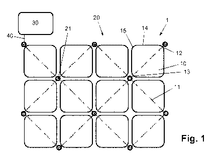
Fig. 1 relates to a light emitting device 1 according to a first embodiment of
the invention, comprising light emitting units 10 being arranged in a plane
filling pattern 20,
.. so that the light emitting device 1 is suitable to be used for covering at
least a substantial
portion of a surface. The light emitting units 10 are generally shaped like a
tile, panel or the
like, and comprise an internal electrical circuit 11 as diagrammatically
indicated by means of
dashed lines crossing the light emitting units 10. Also, in the shown
embodiment, the light
emitting units 10 comprise two connection areas 12, 13 providing electrical
access to the
.. internal electrical circuit 11 from outside of the light emitting units 10.
The internal electrical
circuit 11 may be configured in any appropriate way. For example, it may be so
that the light
emitting units 10 are equipped with at least one light source, and that the
internal electrical
circuit 11 comprises a plus wire and a minus wire for powering the at least
one light source,
wherein the at least one light source is arranged between the wires. Also, the
connection
areas 12, 13 may be configured in any appropriate way, as long as the function
of providing a
position where a light emitting unit 10 can be electrically interconnected to
at least one other
light emitting unit 10 is fulfilled. In this respect, it is noted that it is
practical for the
connection areas 12, 13 to comprise at least one electrically conductive
member of some sort.
CA 03071730 2020-01-31
WO 2019/025230 PCT/EP2018/069981
17
In any case, in the light emitting device 1, the light emitting units 10 are
electrically
interconnected through the connection areas 12, 13 thereof.
In the shown embodiment, the light emitting units 10 have a generally square
periphery, wherein the light emitting units 10 have four sides 14 and four
corners 15
interconnecting the sides 14. It is to be noted that this particular shape of
the light emitting
units 10 is shown for illustration purposes only, and that the present
disclosure is not limited
to such a shape in any way. Other possible shapes are shown in Figs. 5-7, as
will be
explained later. Fig. 1 illustrates the option of providing the light emitting
units 10 with
rounded corners 15, which does not alter the fact that within the framework of
the invention,
the corners 15 may as well be sharp. Further, in the shown example, the
pattern 20 of light
emitting units 10 is of a regular character, the light emitting units 10 being
arranged in
columns and rows at a certain small mutual distance. These features of the
pattern 20 are not
essential; particularly, the light emitting units 10 may as well be arranged
in an abutting
fashion. As far as the positioning of the connection areas 12, 13 on the light
emitting units 10
is concerned, it is noted that the connection areas 12, 13 are situated at two
opposite corners
15 of the light emitting unit 10 in the shown example.
In Fig. 1, only a few of a total number of light emitting units 10 of the
light
emitting device 1 are shown. Within the framework of the invention, the light
emitting device
1 may comprise any suitable number of light emitting units 10, wherein it is
possible for the
number of light emitting units 10 to be as high as 10,000, or even (far) more.
The light
emitting units 10 may have any suitable dimensions. In view of a practical
possibility of
using the light emitting device 1 for the purpose of covering a ship's hull
and performing an
anti-fouling action by emitting anti-fouling light in a direction away from
the hull, an
example of such dimensions are dimensions in the order of 1 m when it comes to
a length of
the sides 14 of the light emitting units 10.
The light emitting units 10 may be of any suitable design and may comprise
any suitable components, depending on the intended use of the light emitting
device 1. An
example of intended use of the light emitting device 1 is use for the purpose
of performing an
anti-fouling action on surfaces, as mentioned, wherein it is advantageous if
the device 1 is
designed to emit ultraviolet light during operation thereof. In such a case,
it may be practical
for the device 1 to be designed to specifically emit ultraviolet light of the
c type, which is
also known as UVC light, and even more specifically, light with a wavelength
roughly
between 250 nm and 300 nm. It has been found that most fouling organisms are
killed,
rendered inactive, or rendered unable to reproduce by exposing them to a
certain dose of
CA 03071730 2020-01-31
WO 2019/025230 PCT/EP2018/069981
18
ultraviolet light having such characteristics. The light may be applied
continuously or at a
suitable frequency, whatever is appropriate in a given situation, especially
at a given light
intensity. Also, in such a case, it may be practical for the light emitting
units 10 to comprise
silicone material.
In general, the light emitting units 10 may comprise at least one light source
(not shown) for emitting the light that is envisaged, and further an internal
electric track
and/or internal electric wiring as part of the internal electrical circuit 11,
to which the at least
one light source is connected. For the purpose of powering the at least one
light source of the
light emitting units 10, the light emitting device 1 comprises an electric
power source 30, and
the light emitting units 10, particularly the internal electrical circuit 11
thereof, are connected
to that power source 30. As mentioned in the foregoing, the light emitting
units 10 are
electrically interconnected through the connection areas 12, 13 thereof. The
light emitting
device 1 comprises at least one electrically conductive element 40 for
electrically
interconnecting at least one of the light emitting units 10 and the power
source 30. As the
other light emitting units 10 are electrically connected to the at least one
of the light emitting
units 10 that is directly connected to the power source 30, all other light
emitting units 10 are
indirectly connected to the power source 30 as well, so that only one power
source 30 is
needed for powering a large number of light emitting units 10.
In the light emitting device 1 shown in Fig. 1, electrical connections are
provided between four light emitting units 10 at one position. In the present
text, in view of
the fact that the electrical connections involve more than a conventional
number of two light
emitting units 10, the electrical connections are referred to as combined
connections.
Positions where the combined connections are provided are positions where four
light
emitting units 10 meet, i.e. positions both between two rows and between two
columns,
which will hereinafter be referred to as nodal positions 21. Not all nodal
positions 21 between
the light emitting units 10 as present in the pattern 20 are positions where
four light emitting
units 10 are interconnected. The combined connections are only provided at the
nodal
positions 21 where connection areas 12, 13 of four light emitting units 10
come together. As
a consequence, in the shown example, the combined connections are provided at
every other
nodal position 21, both in the direction of the rows and the direction of the
columns of the
pattern 20.
The combined connections between four light emitting units 10 at respective
nodal positions 21 can be realized in any suitable way. In the first place, it
is possible to have
at least one actual conductive element interconnecting the connection areas
12, 13 of the
CA 03071730 2020-01-31
WO 2019/025230 PCT/EP2018/069981
19
respective light emitting units 10. Such an electrically conductive element
may be provided
as wiring, but other possibilities exist within the framework of the invention
as well,
including a possibility of the electrically conductive element being provided
as a bump or
track of an electrically conductive material. In the case of wiring, it may be
practical for the
wiring to be of the twin type, providing a plus wire and a minus wire for
powering the at least
one light source of the light emitting units 10, although it is also possible
to have separate
plus wires and minus wires. Assuming that separate plus and minus wires are
used in a light
emitting unit 10, those wires may be arranged so as to extend more or less in
a parallel
configuration through the light emitting unit 10, in which case the wires may
extend between
.. the same connection areas 12, 13 of the light emitting unit 10 so that the
number of
connection areas 12, 13 of the light emitting unit 10 can remain as low as
possible. This is
however not essential within the framework of the invention. For example, it
is also possible
to have a cross-like configuration of the wires, in which the plus wire
extends between two
other connection areas 12, 13 of the light emitting unit 10 than the minus
wire.
If the light emitting device 1 is intended to be used underwater, it is
practical if
measures are taken for having a liquid-tight seal at the positions where the
electrically
conductive elements are connected to the light emitting units 10, i.e. the
positions where
electric wires enter/exit the light emitting units 10 in case the electrically
conductive
elements are provided as wiring. The electrically conductive elements arranged
at a nodal
position 21 between four light emitting units 10 may comprise a wire assembly
of two
electric wires in a crosswise arrangement, for example, wherein the electric
wires are
electrically connected to each other at the cross-over position, and wherein
each of the light
emitting units 10 is connected to a respective wire end of the wire assembly,
which does not
alter the fact that other embodiments of those electrically conductive
elements are also
feasible. A practical alternative to using wiring for electrically
interconnecting the light
emitting units 10 will be explained later on the basis of Figs. 9-21.
By providing combined connections between the light emitting units 10, it is
achieved that the number of physical connections between the light emitting
units 10 can be
kept to a minimum while at the same time maintaining an acceptable level of
electrical
redundancy in the light emitting device 1. In the case as illustrated in Fig.
1, compared to a
conventional situation in which each connection is only between two light
emitting units 10,
it is achieved that the total number of connections between light emitting
units 10 in the light
emitting device 1 can be reduced by roughly 50% while still having the same
level of
electrical redundancy, so that it is guaranteed that each of the light
emitting units 10 is at a
CA 03071730 2020-01-31
WO 2019/025230 PCT/EP2018/069981
position for receiving power through alternative connection routes, as a
result of which
failure of a light emitting unit 10 or a connection to a light emitting unit
10 does not affect
the functioning of the other light emitting units 10. In other words, it is
possible to have quite
a number of failing light emitting units 10 and/or failing connections to
light emitting units
5 10 and still have a maximum number of operative light emitting units 10.
The fact is that in
the light emitting device 1, individual light emitting units 10 can be reached
by electric power
at two positions on the light emitting unit 10, namely at two opposite corner
positions. When
one of the connections to a light emitting unit 10 fails, the light emitting
unit 10 can still be
powered through an alternative route. In Fig. 1, the routing of the electric
power through the
10 pattern 20 of light emitting units 10 is through the internal electrical
circuit 11 of the
respective light emitting units 10 and the combined connections between the
light emitting
units 10 at nodal positions 21 in the pattern 20. In general, it is to be
noted that in the light
emitting device 1, the power is provided through a grid-shaped routing
structure offering
many different alternative routes.
15 The suggestion that the amount of connections between light
emitting unit 10
can be kept to a minimum, while still an acceptable level of electrical
redundancy is
maintained, can be further understood by making a comparison between the light
emitting
device 1 as shown in Fig. 1 and respective conventional light emitting devices
200, 300, 400
as shown in Figs. 2, 3 and 4.
20 In Fig. 2, a conventional light emitting device 200 is shown in
which every
light emitting unit 10 is individually connected to an electric power source
30 (not shown in
Fig. 2) through an electrically conductive element 40 in the form of an
electric wire. In this
layout, when a connection to one of the light emitting units 10 fails, that
particular unit 10
cannot be powered through an alternative route and is no longer useful. On the
other hand,
the power supply to the other light emitting units 10 is not affected.
However, it takes a large
amount of electric wires to achieve this level of electrical redundancy,
wherein most of those
electric wires need to cover relatively large distances and are extra
susceptible to damage as a
result thereof.
In Fig. 3, a conventional light emitting device 300 is shown in which the
light
emitting units 10 are connected in daisy chain fashion, wherein the light
emitting units 10 are
electrically connected one after another, and wherein connections need to be
made at two
sides of each of the light emitting units 10. In conformity with Fig. 1, the
internal electrical
circuits 11 of the respective light emitting units 10 are diagrammatically
indicated by means
of dashed lines in Fig. 3, thereby indicating how the electric power is routed
through the
CA 03071730 2020-01-31
WO 2019/025230 PCT/EP2018/069981
21
pattern 20 of light emitting units 10. The layout shown in Fig. 3 is extremely
vulnerable to
damage. The fact is that if one light emitting unit 10 or connection to a
light emitting unit 10
fails, all of the light emitting units 10 further down the daisy chain cannot
be supplied with
power.
In Fig. 4, a conventional light emitting device 400 is shown in which the
level
of electrical redundancy is improved in comparison to the option of daisy
chaining the light
emitting units 10 as illustrated in Fig. 3. However, this is at the cost of an
increase of the
number of electrical connections that are necessary. As can be seen in Fig. 4,
individual light
emitting units 10 that are at an edge position of the light emitting device
400 are connected to
three other light emitting units 10, with the exception of a light emitting
unit 10 that is at a
corner position of the light emitting device 400, and individual light
emitting units 10 that are
not at an edge position of the light emitting device 400 are connected to four
other light
emitting units 10. Particularly, connections between two adjacent light
emitting units 10 are
provided at a position where sides 14 of the light emitting units 10 face each
other. By
making electrical connections between light emitting units 10 at nodal
positions 21 between
as many as four light emitting units 10, rather than at positions between
sides 14 of only two
light emitting units 10, the same level of electrical redundancy can be
realized while reducing
the amount of connections between light emitting units 10 by 50%.
In conformity with Fig. 1, the internal electrical circuits 11 of the
respective
light emitting units 10 are diagrammatically indicated by means of dashed
lines in Fig. 4,
thereby indicating how the electric power is routed through the pattern 20 of
light emitting
units 10. In the layout shown in Fig. 1, the routing of the electric power is
still grid-shaped,
with square basic elements, as is the case in the conventional option
illustrated in Fig. 4,
which is a further explanation as to why it is possible to have the same level
of electrical
redundancy. The difference is that in the layout shown in Fig. 1, the routing
is through nodal
positions 21 between the light emitting units 10 and is thereby tilted over an
angle of 45
with respect to a conventional routing through the sides 14 of the light
emitting units 10.
Fig. 5 relates to a light emitting device 2 according to a second embodiment
of
the invention. In this light emitting device 2, the light emitting units 10
are diamond-shaped,
and combined connections are provided between three light emitting units 10.
The light
emitting units 10 are shown as being arranged in an abutting fashion, whereas
in practical
cases, the light emitting units 10 may be arranged with some space between the
sides 14
thereof.
CA 03071730 2020-01-31
WO 2019/025230 PCT/EP2018/069981
22
As is the case with the configuration shown in Fig. 1, the light emitting
units
do not need to comprise more than two connection areas 12, 13, wherein the
connection
areas 12, 13 are located at opposite corner positions on the light emitting
units 10, although
the latter is not essential. Fig. 5 further illustrates the fact that the
electric routing through the
5 light emitting device 2 can be depicted as a grid comprising hexagonal
basic elements,
wherein, in a number of light emitting units 10, the two connection areas 12,
13 of the light
emitting units 10 are shown as being interconnected through a straight line
crossing the light
emitting units 10 from one connection area 12 to the other connection area 13,
representing
the internal electrical circuit 11 of the light emitting units 10. Thus, the
electrical redundancy
10 .. is at a level as desired, wherein a light emitting unit 10 can still be
used when a connection to
that light emitting unit 10 fails, and the functioning of the other light
emitting units 10 is not
affected either, while the number of connections to each of the light emitting
units 10 is
minimal.
Fig. 6 relates to an alternative light emitting device 3. In this light
emitting
device 3, the light emitting units 10 are generally square-shaped, having a
cut-out at two
opposite corner positions, and a connection area 12, 13 at each of the cut-
outs. The light
emitting units 10 are shown as being arranged in an abutting fashion, which
does not alter the
fact that the light emitting units 10 may be arranged with some space between
the sides 14
thereof. In the pattern 20, the light emitting units 10 are arranged such that
square spaces 22
are obtained between the light emitting units 10 at the position of the cut-
outs of the light
emitting units 10. Four light emitting units 10 are electrically
interconnected at the position
of the spaces 22. In particular, the spaces 22 may be used for accommodating
electrically
conductive elements 40 such as electric wires as may be used for electrically
interconnecting
four light emitting units 10.
In fact, the alternative light emitting device 3 resembles the light emitting
device 1 according to the first embodiment of the invention to a large extent,
a difference
pertaining to the shape of the light emitting units 10 at the opposite corner
positions where
the connection areas 12, 13 of the light emitting units 10 are located. On the
basis of the fact
that the light emitting units 10 are provided with cut-outs, it is possible,
but not necessary, to
arrange the light emitting units 10 in a closely adjoining fashion and still
have sufficient
room for accommodating electrically conductive elements 40 between the light
emitting units
10, namely at the positions of the square spaces 22. According to one
possibility existing
within the context of the alternative light emitting device 3, such
electrically conductive
elements 40 may comprise a length of electric wire having split ends for
connection to two
CA 03071730 2020-01-31
WO 2019/025230 PCT/EP2018/069981
23
light emitting units 10 at each of the ends. In Fig. 6, this possibility is
diagrammatically
depicted, whereas, in conformity with Fig. 1, the way in which the connection
areas 12, 13 of
the light emitting units 10 are electrically interconnected through the
internal electrical circuit
11 of the light emitting units 10 is indicated by means of dashed lines, as a
result of which the
grid-like structure of the electric routing through the pattern 20 is clearly
visible in Fig. 6.
Fig. 7 relates to a light emitting device 4 according to a third embodiment of
the invention. In this light emitting device 4, the light emitting units 10
are triangular-shaped.
It is noted that in Fig. 7, the light emitting units 10 are shown as being
arranged in an
abutting fashion, whereas in practical cases, the light emitting units 10 may
be arranged with
some space between the sides 14 thereof.
The pattern 20 shown in Fig. 7 is an example of a pattern 20 in which the
light
emitting units 10 are electrically interconnected both through conventional
connections
between two light emitting units 10 and through combined connections between
more than
two light emitting units 10, namely between as many as six light emitting
units 10 in this
particular case. In particular, each of the light emitting units 10 is
connected to five other
light emitting units 10 at a corner 15 thereof, and to one further light
emitting unit 10 at a
position on a side 14 opposite to the corner 15 as mentioned. The grid-like
structure of the
electric routing through the pattern 20 is also shown in Fig. 7, comprising
triangular basic
elements having sides extending between the positions of the combined
connections. It is a
fact that also in the layout shown in Fig. 7, each of the light emitting units
10 does not
comprise more than two connection areas 12, 13, while sufficient electrical
redundancy is
still guaranteed through combined connections between more than two light
emitting units
10, namely six light emitting units 10 in this particular case.
Fig. 8 relates to a light emitting device 5 according to a fourth embodiment
of
the invention. In this light emitting device 5, the light emitting units 10
are generally square-
shaped. The light emitting units 10 are shown as being arranged at a short
mutual distance,
which does not alter the fact that the light emitting units 10 may as well be
arranged in an
abutting fashion.
In fact, the light emitting device 5 according to the fourth embodiment of the
invention resembles the light emitting device 1 according to the first
embodiment of the
invention to a large extent, a difference pertaining to the positioning of the
connection areas
12, 13 on the light emitting units 10. Fig. 8 serves to illustrate the fact
that it is not necessary
for the connection areas 12, 13 to be located at corner positions on the light
emitting units 10,
showing a pattern 20 of light emitting units 10 in which combined connections
are provided
CA 03071730 2020-01-31
WO 2019/025230 PCT/EP2018/069981
24
between four light emitting units 10, in a similar manner as is the case in
the light emitting
device 1 according to the first embodiment of the invention, but in which
light emitting units
are used that have their connection areas 12, 13 positioned at opposite sides
14 thereof. In
this embodiment, it may be practical for the light emitting units 10 to be
electrically
5 interconnected through electric wiring or electrically conductive tracks,
for example. In any
case, this embodiment also has the feature of no more than two connection
areas 12, 13 per
light emitting unit 10 and an arrangement of combined connections at (or near)
every other
nodal position 21 only, while still having the same level of electrical
redundancy as the
conventional option illustrated in Fig. 4 that needs twice as many
connections. It is noted that
10 in the case of generally square-shaped light emitting units 10, in which
combined connections
of four light emitting units 10 are provided, it appears to be sufficient for
the number of
combined connections to be 50% of the number of light emitting units 10.
Figs. 9-17 relate to a light emitting unit 10 having recessed portions 16
where
connection areas 12, 13 of the light emitting unit 10 are located, and Fig. 18
relates to an
alternative configuration of a connection area 12, 13 on a recessed portion 16
of a light
emitting unit 10.
In Fig. 9, a single light emitting unit 10 having a generally square periphery
is
shown. In this embodiment, the light emitting unit 10 has two recessed
portions 16, located at
two opposite corner positions on the light emitting unit 10. The connection
areas 12, 13 are
provided at the position of the recessed portions 16 in the form of an
electrically conductive
strip 17 that is in electrical connection with the internal electrical circuit
11 of the light
emitting unit 10. The two recessed portions 16 are located at different
levels, the electrically
conductive strip 17 of one of the recessed portions 16 facing upward, and the
electrically
conductive strip 17 of the other of the recessed portions 16 facing downward.
The recessed
portions 16 partially extend from the generally square periphery of the light
emitting unit 10
so as to enable a partially overlapping arrangement of the light emitting
units 10 at the very
positions of the recessed portions 16 thereof as will now be explained with
reference to Figs.
10-17, which serve to illustrate a process of putting four identical light
emitting units 10a,
10b, 10c, 10d together for the purpose of making a combined connection between
the light
emitting units 10a, 10b, 10c, 10d.
In Fig. 10, a first light emitting unit 10a is partially shown, with one of
the
recessed portions 16 extending forward as seen in the figure.
In Fig. 11, it is illustrated how a second light emitting unit 10b is
positioned
with respect to the first light emitting unit 10a, namely with a recessed
portion 16 extending
CA 03071730 2020-01-31
WO 2019/025230 PCT/EP2018/069981
backward as seen in the figure, at a position beside the recessed portion 16
of the first light
emitting unit 10a, wherein the electrically conductive strips 17 as present on
the recessed
portions 16 of the light emitting units 10a, 10b extend substantially parallel
to each other.
Figs. 12 and 13 show how a third light emitting unit 10c is positioned with
5 .. respect to both the first light emitting unit 10a and the second light
emitting unit 10b, wherein
it is noted that in these figures, hidden parts of the electrically conductive
strips 17 and tracks
31 of the internal electrical circuit 11 of the light emitting units 10a, 10b,
10c, leading from
the strips 17 to inside the light emitting units 10a, 10b, 10c, are indicated
by means of dotted
lines. Fig. 12 shows the third light emitting unit 10c approaching the first
light emitting unit
10 10a and the second light emitting unit 10b, and Fig. 13 shows the third
1 light emitting unit
10c (almost) in place with respect to the first light emitting unit 10a and
the second light
emitting unit 10b.
With respect to the recessed portions 16 of the first light emitting unit 10a
and
the second light emitting unit 10b, the recessed portion 16 of the third light
emitting unit 10c
15 is oriented upside down, with the electrically conductive strip 17
thereof extending at an
angle of substantially 90 with respect to the respective strips 17 of the
first light emitting
unit 10a and the second light emitting unit 10b. As a result, it is achieved
that the recessed
portion 16 of the third light emitting unit 10c overlaps half of the
respective recessed portions
16 of the first light emitting unit 10a and the second light emitting unit
10b, wherein the
20 electrically conductive strip 17 of the third light emitting unit 10c
faces the respective strips
17 of the first light emitting unit 10a and the second light emitting unit
10b, and wherein the
portions of the light emitting units 10a, 10b, 10c outside of the recessed
portions 16 extend in
one and the same plane, so that a light emitting device having an even overall
surface can be
realized.
25 Figs. 14-17 show how a fourth light emitting unit 10d is
positioned with
respect to the first light emitting unit 10a, the second light emitting unit
10b and the third
light emitting unit 10c. Figs. 14 and 15 show the fourth light emitting unit
10d approaching
the first light emitting unit 10a, the second light emitting unit 10b and the
third light emitting
unit 10c, and Figs. 16 and 17 show the fourth light emitting unit 10d in place
with respect to
the first light emitting unit 10a, the second light emitting unit 10b and the
third light emitting
unit 10c. In Figs. 14 and 16, hidden parts of the electrically conductive
strips 17 and the
tracks 31 of the internal electrical circuit 11 of the light emitting units
10a, 10b, 10c, 10d are
indicated by means of dotted lines, whereas Figs. 15 and 17 illustrate the
actual view on the
light emitting units 10a, 10b, 10c, 10d.
CA 03071730 2020-01-31
WO 2019/025230 PCT/EP2018/069981
26
As is the case with the recessed portion 16 of the third light emitting unit
10c,
the recessed portion 16 of the fourth light emitting unit 10d is oriented
upside down with
respect to the recessed portions 16 of the first light emitting unit 10a and
the second light
emitting unit 10b, with the electrically conductive strip 17 thereof extending
at an angle of
substantially 90 with respect to the respective strips 17 of the first light
emitting unit 10a and
the second light emitting unit 10b, and extending substantially parallel to
the strip 17 of the
third light emitting unit 10c. In fact, a space that remains on the
combination of the recessed
portions 16 of the first light emitting unit 10a and the second light emitting
unit 10b after the
third light emitting unit 10c has been put in place, is filled and closed by
means of the
recessed portion 16 of the fourth light emitting unit 10d, wherein the fourth
light emitting
unit 10d is made to approach from an opposite side than the third light
emitting unit 10c.
By putting the four light emitting units 10a, 10b, 10c, 10d together in the
way
as described in the foregoing and as illustrated in Figs. 10-17, it is
achieved that the closed
configuration as shown Figs. 16 and 17 is obtained as an end result. In the
process, the
recessed portions 16 of the light emitting units 10a, 10b, 10c, 10d are made
to overlap, in
such orientations that a crosswise configuration of two substantially parallel
electrically
conductive strips 17 at a bottom level and two substantially parallel
electrically conductive
strips 17 at a top level is obtained, the strips 17 of the two levels facing
each other. In this
way, a combined connection of the four light emitting units 10a, 10b, 10c, 10d
is realized. In
the shown example, the recessed portions 16 of the light emitting units 10a,
10b, 10c, 10d are
about half as high as the larger portions of the light emitting units 10a,
10b, 10c, 10d, i.e. the
portions of the light emitting units 10a, 10b, 10c, 10d outside of the
recessed portions 16, so
that a light emitting device having an even overall surface is realized, as
mentioned earlier.
In the combined connection of the four light emitting units 10a, 10b, 10c,
10d,
the electrically conductive strip 17 of the first light emitting unit 10a
faces parts of the strips
17 of the third light emitting unit 10c and the fourth light emitting unit
10d, and is associated
with the strip 17 of the second light emitting unit 10b through the strips 17
of the third light
emitting unit 10c and the fourth light emitting unit 10d. Likewise, the
electrically conductive
strip 17 of the second light emitting unit 10b faces parts of the strips 17 of
the third light
emitting unit 10c and the fourth light emitting unit 10d, and is associated
with the strip 17 of
the first light emitting unit 10a through the strips 17 of the third light
emitting unit 10c and
the fourth light emitting unit 10d, the electrically conductive strip 17 of
the third light
emitting unit 10c faces parts of the strips 17 of the first light emitting
unit 10a and the second
light emitting unit 10b, and is associated with the strip 17 of the fourth
light emitting unit 10d
CA 03071730 2020-01-31
WO 2019/025230 PCT/EP2018/069981
27
through the strips 17 of the first light emitting unit 10a and the second
light emitting unit 10b,
and the electrically conductive strip 17 of the fourth light emitting unit 10d
faces parts of the
strips 17 of the first light emitting unit 10a and the second light emitting
unit 10b, and is
associated with the strip 17 of the third light emitting unit 10c through the
strips 17 of the
first light emitting unit 10a and the second light emitting unit 10b.
It may be so that the light emitting units 10a, 10b, 10c, 10d are designed
such
that all it takes for having an effective combined connection, through which
an electrical
interconnection of the light emitting units 10a, 10b, 10c, 10d is established,
is putting the
light emitting units 10a, 10b, 10c, 10d together in the way as described in
the foregoing. This
is the case when the electrically conductive strips 17 of the light emitting
units 10a, 10b, 10c,
10d are made to contact each other in the process, or are made to extend
sufficiently close to
each other so that transfer of electric power between the light emitting units
10a, 10b, 10c,
10d can take place on the basis of capacitive effects, for example. On the
other hand, it may
be so that the process of putting the light emitting units 10a, 10b, 10c, 10d
together is
followed by an action of pressing the light emitting units 10a, 10b, 10c, 10d
together at the
position where their recessed portions 16 overlap, an action of supplying heat
to that position,
etc. Optionally, as an intermediate step, glue or solder may be added to the
electrically
conductive strips 17, etc.
It may be practical for the connection areas 12, 13 to comprise two
electrically
conductive strips 17, 18, wherein one of the strips 17, 18 is associated with
a plus side of the
internal electrical circuit 11, and wherein the other of the strips 17, 18 is
associated with a
minus side of the internal electrical circuit 11. Fig. 18 illustrates this
option, particularly by
showing a connection area 12 comprising two electrically conductive strips 17,
18, as
arranged on a recessed portion 16 of a light emitting unit 10. The light
emitting unit 10 in
question is intended to be combined with four other identical light emitting
units 10, in the
same manner as described in the foregoing and illustrated in Figs. 10-17, the
difference
following from the design of the connection areas 12, 13 being a realization
of separate plus
and minus circuits in the combined connections. In order to avoid
interconnection of the plus
and minus circuits, an electrically insulating cover plate 19 is arranged at
an appropriate
position on one of the electrically conductive strips 17, 18. Further, in the
shown example,
the electrically conductive strips 17, 18 are provided with solder areas 32 at
ends thereof.
As explained, the option of having recessed portions 16 and connection areas
12, 13 located on the recessed portions 16 is advantageous in the context of
realizing
combined connections between at least three light emitting units 10. However,
that does not
CA 03071730 2020-01-31
WO 2019/025230 PCT/EP2018/069981
28
imply that this option is limited to such a context. In particular, this
option is also applicable
in a conventional context of realizing connections between no more than two
light emitting
units 10. Further, it is to be noted that the option of having a design of the
light emitting units
including recessed portions 16 is independent of the general shape of the
light emitting
5 units 10.
Within the framework of the invention, putting to practice the option of
having
recessed portions 16 and connection areas 12, 13 located on the recessed
portions 16 may
alternatively comprise a design of the light emitting units 10 that allows for
making the
combined connections by positioning all protruding portions of the light
emitting units 10
10 involved in the combined connections beside each other, at the same
level, and
interconnecting the respective connection areas 12, 13 by means of an
intermediate plate or
the like having an electrical circuit that is made to contact all of the
connection areas 12, 13,
for example. In such a case, it is possible for the connection areas 12, 13 to
be arranged on
portions protruding from the general shape of light emitting units 10. Another
possibility is
that the light emitting units 10 are provided with recessed portions 16 that
are located within
the general shape of the light emitting units 10. This possibility is
illustrated in Figs. 19-21,
as will now be explained.
Fig. 19 shows corner portions of four light emitting units 10a, 10b, 10c, 10d,
particularly corner portions where a recessed portion 16 is present on the
respective light
emitting units 10a, 10b, 10c, 10d. The four light emitting units 10a, 10b,
10c, 10d are
arranged in such a way that the respective recessed portions 16 extend beside
each other, at
the same level, with a connection area 12 as present on the respective
recessed portions 16
being accessible from one and the same side. In the present example, as is the
case with the
example shown in Figs. 9-17, the connection area 12 of each of the light
emitting units 10a,
10b, 10c, 10d is provided at the position of the recessed portion 16 of the
respective light
emitting unit 10a, 10b, 10c, 10d in the form of an electrically conductive
strip 17 that is in
electrical connection with the internal electrical circuit 11 of the light
emitting unit 10a, 10b,
10c, 10d.
Fig. 20 illustrates how a plate 50 comprising an electrical circuit 51 that is
accessible from the outside at the positions of four contacting pads 52 is
made to approach a
recessed area defined by the four recessed portions 16 of the respective light
emitting units
10a, 10b, 10c, 10d. The plate 50 is put down on this recessed area, wherein
each of the four
contacting pads 52 are made to face or contact an electrically conductive
strip 17 of another
light emitting unit 10a, 10b, 10c, 10d, whereby a combined connection between
the light
CA 03071730 2020-01-31
WO 2019/025230 PCT/EP2018/069981
29
emitting units 10a, 10b, 10c, 10d, in which the light emitting units 10a, 10b,
10c, 10d are
electrically interconnected through the electrical circuit 51 of the plate 50,
can be established.
The final position of the plate 50 with respect to the light emitting units
10a, 10b, 10c, 10d is
illustrated in Fig. 21. As shown, it may be practical if the dimensions of the
plate 50 are
chosen such that the plate 50 is capable of covering the entire recessed area,
although this is
not essential within the framework of the invention. Further, as shown, it may
be practical if
the dimensions of the plate 50 are chosen such that the plate 50 can be flush
with the light
emitting units 10a, 10b, 10c, 10d. In general, the dimensions of the plate 50
are preferably
chosen such that the plate 50 exactly fits in the space that is present
between the light
emitting units 10a, 10b, 10c, 10d at the position of the recessed portions 16
thereof when the
light emitting units 10a, 10b, 10c, 10d have been positioned with respect to
each other in an
appropriate way, as shown in Fig. 19.
In conformity with that which has already been explained in respect of the
example as illustrated in Figs. 9-17, it may be so that the light emitting
units 10a, 10b, 10c,
10d and the plate 50 are designed such that all it takes for realizing an
effective combined
connection of the light emitting units 10a, 10b, 10c, 10d, is putting the
light emitting units
10a, 10b, 10c, 10d and the plate 50 together in the way as described in the
foregoing. This is
the case when the contacting pads 52 of the plate 50 are made to contact the
electrically
conductive strips 17 of the light emitting units 10a, 10b, 10c, 10d in the
process, or are made
to extend sufficiently close to the electrically conductive strips 17 of the
light emitting units
10a, 10b, 10c, 10d. On the other hand, it may be so that the process of
putting the light
emitting units 10a, 10b, 10c, 10d and the plate 50 together is followed by an
action of
pressing the light emitting units 10a, 10b, 10c, 10d and the plate 50 together
at the position
where the plate overlaps the recessed portions 16 of the light emitting units
10a, 10b, 10c,
10d, an action of supplying heat to that position, etc. Optionally, as an
intermediate step, glue
or solder may be added to the electrically conductive strips 17 of the light
emitting units 10a,
10b, 10c, 10d and/or the contacting pads 52 of the plate 50, etc.
Further, it may be practical for the connection area 12 of the respective
light
emitting units 10a, 10b, 10c, 10d to comprise two electrically conductive
strips 17, 18,
wherein one of the strips 17, 18 is associated with a plus side of the
internal electrical circuit
11, and wherein the other of the strips 17, 18 is associated with a minus side
of the internal
electrical circuit 11. In such a case, it may be appropriate for the
electrical circuit 51 of the
plate 50 to comprise a plus portion and a minus portion, generally at
different positions/levels
in the plate 50. The plate 50 may only be used for interconnecting the four
light emitting
CA 03071730 2020-01-31
WO 2019/025230 PCT/EP2018/069981
units 10a, 10b, 10c, 10d, but it is also possible for the plate 50 to have
additional
functionalities. For example, the plate 50 may be equipped with at least one
functional
component such as a light source. This aspect of the plate 50 is independent
of other features
of the plate 50 such as size and shape, and also of the exact number of the
light emitting units
5 10a, 10b, 10c, 10d to be electrically interconnected through the plate
50.
It will be clear to a person skilled in the art that the scope of the
invention is
not limited to the examples discussed in the foregoing, but that several
amendments and
modifications thereof are possible without deviating from the scope of the
invention as
defined in the attached claims. It is intended that the invention be construed
as including all
10 such amendments and modifications insofar they come within the scope of
the claims or the
equivalents thereof. While the invention has been illustrated and described in
detail in the
figures and the description, such an illustration and such a description are
to be considered
illustrative or exemplary only, and not restrictive. The invention is not
limited to the
disclosed embodiments. The drawings are schematic, wherein details that are
not required for
15 understanding the invention may have been omitted, and not necessarily
to scale. As the
invention is not particularly about the connection of a pattern 20 of light
emitting units 10 to
an electric power source 30 of a light emitting device 1, 2, 3, 4, 5, but
rather relates to a
clever way for electrically interconnecting the light emitting units 10, a
depiction of an
electric power source 30 is only provided in Fig. 1. For the sake of
completeness, it is noted
20 that this fact should not be understood so as to mean that the other
embodiments of the
invention do not include an electric power source 30 as well.
Variations to the disclosed embodiments can be understood and effected by a
person skilled in the art in practicing the claimed invention, from a study of
the figures, the
description and the attached claims. In the claims, the word "comprising" does
not exclude
25 other steps or elements, and the indefinite article "a" or "an" does not
exclude a plurality.
Any reference signs in the claims should not be construed as limiting the
scope of the
invention.
Elements and aspects discussed for or in relation with a particular embodiment
may be suitably combined with elements and aspects of other embodiments,
unless explicitly
30 stated otherwise. Thus, the mere fact that certain measures are recited
in mutually different
dependent claims does not indicate that a combination of these measures cannot
be used to
advantage.
The term "comprise" as used in this text will be understood by a person
skilled
in the art as covering the term "consist of'. Hence, the term "comprise" may
in respect of an
CA 03071730 2020-01-31
WO 2019/025230 PCT/EP2018/069981
31
embodiment mean "consist of', but may in another embodiment mean
"contain/include at
least the defined species and optionally one or more other species".
A possible summary of the invention reads as follows. A light emitting device
1, 2, 4, 5 is provided that can be used in various contexts, including the
context of realizing
an anti-fouling action on surfaces. The light emitting device 1, 2, 4, 5
comprises light
emitting units 10 being arranged in a plane filling pattern 20 for covering at
least a substantial
portion of a surface. Individual light emitting units 10 are electrically
interconnected through
connection areas 12, 13 as present on the light emitting units 10 for
providing electrical
access to an internal electrical circuit 11 thereof, wherein the light
emitting units 10 overlap
at the positions of at least portions of the connection areas 12, 13 thereof.
Further, it may be
so that at least one of the connection areas 12, 13 of the individual light
emitting units 10 is
electrically connected simultaneously to respective connection areas 12, 13 of
at least two
other light emitting units 10, so as to have an acceptable, practical level of
electrical
redundancy in the light emitting device 1, 2, 3, 4, 5 at only a minimum of
electrical
.. connections in the light emitting device 1, 2, 3, 4, 5.