Note: Descriptions are shown in the official language in which they were submitted.
CA 03072017 2020-02-03
WO 2019/032488 PCT/US2018/045477
SENSORS IMPLANTABLE INTO A PATIENT'S BODY, SYSTEMS, AND METHODS OF
USING THE SAME
CROSS-REFERENCE TO RELATED APPLICATIONS
[0001] This application claims the benefit of U.S. Provisional Application
Serial No.
62/541,924, filed August 7, 2017, the disclosure of which is hereby
incorporated by reference as
if set forth in its entirety herein.
TECHNICAL FIELD
[0002] The present invention relates to sensors that are implantable into a
patient's
body, and to systems and methods of using the same.
BACKGROUND
[0003] Tracking of physical disease and healing in humans often involves
measuring
anatomical properties of a patient's body. However, some measurements, such as
those that can
only be obtained internally, can be difficult to obtain. More recently, there
has been an interest
in sensors that can be implanted into a patient's body to track the health of
the patient over time.
For example, attempts have been made to use one or more strain gauges to track
healing in a
damaged or fractured bone. The one or more strain gauges are attached to an
orthopedic implant
that is in turn attached to the damaged or fractured bone. As the bone heals,
the bone
increasingly shares the load imparted by the patient's body on the orthopedic
implant. Thus, the
load imparted on the bone increases as the bone heals, while the load imparted
on the orthopedic
implant decreases. In principle, this change in loading can be measured over
time by the one or
1
CA 03072017 2020-02-03
WO 2019/032488 PCT/US2018/045477
more strain gauges to track the progress of healing in the bone. The
measurement can then be
communicated to a device outside of the body that can be accessed by a
physician.
SUMMARY
[0004] In one example, a sensor that is configured to be implanted into a
patient's body
comprises at least one sensing element, a measurement device in communication
with the at least
one sensing element, and an internal wireless communicator in communication
with the
measurement device. The at least one sensing element includes a resistor, and
the measurement
device includes at least one capacitor. Further, the measurement device is
configured to measure
a discharge time of the at least one capacitor through the resistor so as to
generate a measurement
value that is proportional to a value of an anatomical property of the
anatomical body observed
by the sensor. The wireless communicator is configured to wirelessly
communicate the
measurement value through skin of the patient to an external wireless
communicator situated
outside of the patient's body.
[0005] In another example, a method detects a value of an anatomical property
of a
patient from at least one sensor implanted into a patient's body. The method
comprises a step of
charging at least one capacitor of the at least one sensor to a reference
voltage. The method
further comprises a step of discharging the at least one capacitor through at
least one resistive
sensing element of the at least one sensor. The method yet further comprises a
step of generating
a measurement value that is proportional to the value of the anatomical
property. The generating
step comprises measuring a discharge time of the at least one capacitor to a
trigger voltage. The
method yet still further comprises a step of wirelessly communicating the
measurement value
through skin of the patient to an external wireless communicator situated
outside of the patient's
body.
[0006] In yet another example, a sensor that is configured to be implanted
into a
patient's body comprises a semiconductor strain gauge with the at least one
sensing element, a
measurement device in communication, and an internal wireless communicator in
communication with the measurement device. The strain gauge has a substrate
and first, second,
and third sensing elements arranged on the substrate such that the first,
second, and third sensing
elements are non-parallel to one another. The measurement device is configured
to generate a
measurement value that is proportional to a value of an anatomical property of
the anatomical
body observed by the sensor. The wireless transmitter is configured to
wirelessly communicate
the measurement value through the skin of the patient to an external wireless
communicator
situated outside of the patient's body.
2
CA 03072017 2020-02-03
WO 2019/032488 PCT/US2018/045477
[0007] In yet still another example, a system comprises an anatomical implant
and first
and second sensors supported by the anatomical implant. The first sensor
includes a first unique
identifier and comprises at least a first sensing element, a first measurement
device in
communication with the at least first sensing element, and a first internal
wireless communicator.
The first measurement device is configured to generate a first measurement
value that is
proportional to a value of an anatomical property of the anatomical body
observed by the first
sensor, and the first internal wireless communicator is configured to
wirelessly communicate the
first measurement value and first unique identifier through skin of a
patient's body to an external
wireless communicator situated outside of the patient's body. The second
sensor includes a
second unique identifier, different from the first unique identifier, and
comprises at least a
second sensing element, a second measurement device in communication with the
at least second
sensing element, and a second internal wireless communicator. The second
measurement device
is configured to generate a second measurement value that is proportional to a
value of an
anatomical property of the anatomical body observed by the second sensor, and
the second
internal wireless communicator is configured to wirelessly communicate the
second
measurement value and second unique identifier through skin of a patient's
body to the external
wireless communicator situated outside of the patient's body.
BRIEF DESCRIPTION OF THE DRAWINGS
[0008] The foregoing summary, as well as the following detailed description of
embodiments of the application, will be better understood when read in
conjunction with the
appended drawings. For the purposes of illustrating the methods and bone
screws of the present
application, there is shown in the drawings representative embodiments. It
should be
understood, however, that the application is not limited to the precise
methods and devices
shown. In the drawings:
[0009] Fig. 1 shows a simplified schematic diagram of a measurement system
according to one example embodiment that is positioned relative to a patient
so as to measure an
anatomical condition of the patient, the system having a sensor supported by
an anatomical
implant and having an external reader that receives measurements from the
sensor;
[0010] Fig. 2 shows a simplified block diagram of the system of Fig. 1
according to one
example embodiment;
[0011] Fig. 3 shows a plan view of a strain gauge according to one example
embodiment that can include the at least one sensing element of the sensor of
Fig. 2;
[0012] Fig. 4 shows a simplified block diagram of the measurement device of
the
sensor of Fig. 2 according to one example embodiment;
3
CA 03072017 2020-02-03
WO 2019/032488 PCT/US2018/045477
[0013] Fig. 5 shows a simplified block diagram of the power device of the
sensor of
Fig. 2 according to one example embodiment;
[0014] Fig. 6 shows a plan view of the antenna of the sensor of Fig. 2
according to one
example embodiment;
[0015] Fig. 7 shows a perspective view of a measurement system attached to an
anatomical body according to one example embodiment, the system comprising an
anatomical
implant and first and second sensors supported by the implant;
[0016] Fig. 8 shows an enlarged perspective view of a lower portion of the
measurement system of Fig. 7;
[0017] Fig. 9 shows a partially-exploded perspective view of the lower portion
of the
measurement system of Fig. 7;
[0018] Fig. 10 shows a simplified flow diagram of a method of operating the
sensor of
Fig. 2 according to one example embodiment;
[0019] Fig. 11 shows a perspective view of a measurement system attached to an
anatomical body according to another example embodiment, the system comprising
an
anatomical implant, a first sensor supported by the implant, and a second
sensor that is not
supported by the implant;
[0020] Fig. 12 shows an exploded perspective view of a lower portion of a
measurement system according to one example embodiment, where the sensor
includes a shield
disposed between the antenna and the implant;
[0021] Fig. 13 shows a plan view of the shield of the sensor of Fig. 12
according to one
example embodiment;
[0022] Fig. 14 shows a plan view of an antenna system according to one example
embodiment that can be used to implement the antenna system of the sensor of
Fig. 12, where
the antenna system includes an antenna coil and a shield coil supported by a
common substrate;
[0023] Fig. 15 shows a cross-sectional view of a portion of the sensor system
of Fig. 12
according to one example embodiment having electrical components that are
disposed between
the antenna and the shield;
[0024] Fig. 16 shows a cross-sectional view of a portion of the sensor system
of Fig. 12
according to another example embodiment, where the shield is disposed between
the antenna and
the electrical components;
[0025] Fig. 17 shows an electrical circuit diagram of the antenna system of
Fig. 12
according to one example embodiment, where the antenna system includes the
antenna and the
shield;
4
CA 03072017 2020-02-03
WO 2019/032488 PCT/US2018/045477
[0026] Fig. 18 illustrates the magnetic field of the antenna system of Fig.
12; and
[0027] Fig. 19 illustrates the electric field of the antenna system of Fig.
12.
DETAILED DESCRIPTION
[0028] Conventional sensors proposed for use in implantation into a patient's
body
have several drawbacks. First, conventional sensors tend to have relatively
high power needs in
order to obtain the level of sensitivity and accuracy needed for the
application. Typically, these
needs are met with relatively large batteries. However, large batteries are
generally not preferred
for implantation because they may contain materials that are harmful to the
human body and
therefore not biocompatible. Further, use of large batteries can impede
miniaturization of the
sensor. Therefore, there is a need for sensors having relatively low power
needs that can be met
with smaller batteries or through energy harvesting techniques, while still
providing sufficient
sensitivity and accuracy.
[0029] Disclosed herein are sensors that are configured to be implanted into a
patient's
body and components thereof Further, disclosed herein are systems that
comprise an anatomical
implant and at least one sensor configured to be supported by the anatomical
implant. Yet
further, disclosed herein are methods of operating such sensors and systems.
[0030] Referring to Fig. 1, a system 10 is shown that is configured to track
health of a
patient over time. In general, the system 10 comprises at least one
implantable sensor 100 that is
configured to be implanted into a patient's body 20. The system can also
comprise an
anatomical implant 114 configured to support the at least one sensor 100. The
anatomical
implant 114 can be any suitable anatomical implant such as (without
limitation) a bone plate, an
intramedullary nail, a bone anchor, a pedicle screw, a spine rod, an
intervertebral implant, and so
on. In addition, the bone plate can comprise any suitable implantable material
such as, without
limitation, a metal such as titanium or a polymer such as polyether ether
ketone (PEEK).
Alternatively, the at least one sensor 100 can be configured to attach
directly to an anatomical
body of the patient without being supported by an anatomical implant.
[0031] The system can further comprise an external wireless reader 116
configured to
wirelessly receive data from the at least one sensor 100 through the skin of
the patient when the
external wireless reader 116 is situated outside of the patient's body. The
data can then be
communicated to a computing device 30 that can be accessed by the patient or a
medical
professional. The computing device 30 can be physically separate from the
external wireless
reader 116 as shown or can be implemented as part of the external wireless
reader 116.
[0032] In at least some embodiments, the external wireless reader 116 can be
configured to wirelessly provide a source of power to the at least one sensor
100. It will be
CA 03072017 2020-02-03
WO 2019/032488 PCT/US2018/045477
understood that systems of the invention may comprise as few as two, and up to
all three, of (1)
the at least one sensor 100, (2) the anatomical implant 114, and (3) the
external wireless reader
116. Further, it will be understood that various embodiments of the invention
can include only
one of (1) the at least one sensor 100, (2) the anatomical implant 114, and
(3) the external
wireless reader 116, as these components can be distributed separately.
[0033] Referring now to Fig. 2, a simplified block diagram of the system of
Fig. 1 is
shown according to one embodiment. The system comprises a sensor 100 that
comprises at least
one sensing element 102, and a measurement device 104 in communication with
the at least one
sensing element 102. Together, the at least one sensing element 102 and
measurement device
104 are configured to generate a measurement value that is proportional to a
value of an
anatomical property that a patient's body observed by the at least one sensing
element 102 when
the sensor 100 is implanted in the patient's body. The anatomical property can
be any suitable
property for tracking the health of a patient such as (without limitation)
strain, load, deflection,
rotation, temperature, pressure, pH level, oxygen level, and so on.
[0034] To generate the measurement value, each sensing element 102 has a
sensor
property having a value that changes in response to a change in a value of the
anatomical
property observed by the sensing element 102. Thus, each sensing element 102
has a sensor
property having a value that is proportional to the value of the anatomical
property. For
example, the sensor property can be resistance, capacitance, inductance,
piezoelectricity, light
behavior, or other suitable sensor property. The measurement device 104 is
configured to detect
or measure the value of the sensor property, and the value of the anatomical
property can be
calculated from the value of the sensor property. In some embodiments, the
value of the
anatomical property can be calculated by multiplying the measured value of the
sensor property
by a constant.
[0035] Each sensing element 102 can be any suitable type of sensing element
for
tracking the health of a patient, and the sensor property can be any suitable
sensor property. For
example, the sensing element can be (without limitation) at least one of a
resistive sensing
element having a resistance that changes in response to a change in the
anatomical property, a
piezoelectric sensing element having a piezoelectric material that changes an
electrical charge in
response to a change in the anatomical property, a capacitive sensing element
having a
capacitance that changes in response to a change in the anatomical property,
an inductive sensing
element having an inductance that changes in response to a change in the
anatomical property, an
optical sensing element, and so on. In one example, and as will be discussed
further below, each
sensing element 102 can be a resistive sensor, the sensor property of each
sensing element 102
6
CA 03072017 2020-02-03
WO 2019/032488 PCT/US2018/045477
can be an electrical resistance of the sensing element 102, and the anatomical
property can be
strain on the anatomical body, where the resistance of each sensing element
102 changes in
response to a change in strain on the anatomical body.
[0036] The sensor 100 can comprise an internal wireless communicator 108 in
communication with the measurement device 104, and an antenna system 109 in
communication
with the internal wireless communicator 108. The antenna system 109 can
include an antenna
110, and optionally can include other components such as a shield as will be
described in further
detail below. The internal wireless communicator 108 is configured to receive
the measurement
value from the measurement device 104 and provide the measurement value to the
antenna 110
in a suitable form for wireless transmission. The internal wireless
communicator 108 can
include a wireless transmitter or transponder that receives the measurement
value from the
measurement device 104 and prepares the measurement value for wireless
transmission. For
example, the wireless communicator 108 can include processing such as (without
limitation) one
or more of (i) memory configured to store the measurement value, (ii) a
digital-to-analog
converter configured to convert the measurement value to analog format, (iii)
a radio-frequency
(RF) modulator configured to modulate the measurement value, (iv) an error-
correction encoder
configured to encode the measurement value, and other processing consistent
with the wireless
technology employed by the sensor 100.
[0037] In one example, the internal wireless communicator 108 can be
configured as a
passive radio-frequency identification (RFID) transponder. Alternatively, the
internal wireless
communicator can be configured using any other wireless communication
technology suitable
for communicating through the skin such as (without limitation) battery-
assisted passive RFID,
active RFID, Bluetooth, and Wi-Fi. The wireless communicator 108 can further
include a
unique identifier (ID) that can be used to distinguish the sensor 100 from
other sensors. In one
example, the unique ID can be an ID of an RFID tag. The antenna 110 is
configured to convert
an electrical signal corresponding to the measurement value from the wireless
communicator 108
into radio waves so as to transmit the measurement value wirelessly through
the patient's skin to
the external wireless reader 116 situated outside of the patient's body.
[0038] The sensor 100 can comprise a power device 106 configured to supply
power to
the measurement device 104 and wireless communicator 108. In at least some
examples, the
power device 106 can include an energy harvesting device configured to capture
energy from a
suitable energy source that is separate from the sensor 100. For example, the
energy source can
be radio waves communicated from the external wireless reader 116.
Alternatively, the power
device 106 can capture energy from the patient's body itself or from another
external source such
7
CA 03072017 2020-02-03
WO 2019/032488 PCT/US2018/045477
as a source external to the patient's body. For example, the energy source can
include (without
limitation) kinetic energy, electric fields, magnetic fields, and so on. In
some embodiments, the
power device 106 can include a battery.
100391 The measurement device 104, power device 106, and wireless communicator
108 can each be implemented on a printed circuit board (PCB) 112, although
embodiments of the
disclosure are not so limited. Further, the measurement device 104, power
device 106, and
wireless communicator 108 can each be implemented as an integrated circuit
(i.e., chip) that is
mounted onto the printed circuit board 112. The at least one sensing element
102, printed circuit
board 112, and antenna 110 can all be supported by the anatomical implant 114
(shown in Fig.
1), which in turn can be attached to an anatomical body of the patient.
Alternatively, the at least
one sensing element 102, printed circuit board 112, and antenna 110 can all be
attached directly
to the anatomical body of the patient.
[0040] The external wireless reader 116 is configured to wirelessly receive
the
measurement value from the at least one sensor 100 through the skin of the
patient when the
external wireless reader 116 is situated outside of the patient's body.
Moreover, in at least some
examples, the external wireless reader 116 can be configured to wirelessly
provide a source of
power to the at least one sensor 100. In at least one such example, the
external wireless reader
116 can be implemented as an RFID reader.
[0041] The external wireless reader 116 can include an antenna 118 and a
wireless
communicator 120. The wireless communicator 120 can include a transmitter and
a receiver.
Thus, the communicator 120 can be considered to be a transceiver. In at least
some
embodiments, the external wireless reader 116 can further include a computing
device 122. The
computing device 122 can be configured to calculate a value of the anatomical
property based on
the measurement value. In one example, the computing device 122 can calculate
the value of the
anatomical property by multiplying the measurement value by a specified
constant.
Alternatively, the computing device 122 can be implemented separately from the
external
wireless reader 116. For example, the computing device 122 can be a computer
configured to
receive the measurement value from the external wireless reader 116 and
present the value to a
physician.
[0042] Referring to Figs. 2 and 3, in one example, the sensor 100 can comprise
a strain
gauge 200 having the at least one sensing element 102. Thus, the at least one
sensing element
102 can be part of the strain gauge 200. Each of the at least one sensing
element 102 can include
a resistor 204. The strain gauge 200 can further include a substrate 202 that
carries the at least
one sensing element 102. Each of the at least one sensing element 102 can be a
semiconductor
8
CA 03072017 2020-02-03
WO 2019/032488 PCT/US2018/045477
bar-type strain gauge similar to those manufactured by Micron Instruments,
where the
semiconductor bar-type strain gauges are arranged on the substrate 202. The
substrate 202 can
be silicon or any other suitable substrate material. The substrate 202 can be
flexible. For
example, the substrate 202 can be implemented as a flexible printed circuit
board. In at least
some embodiments, each of the at least one sensing element 102 can have a
gauge factor in the
range of 100 to 200. Further, in at least some such embodiments, each of the
at least one sensing
element 102 can have a gauge factor in the range of 140 to 160. The effective
gauge factor can
be adjusted by adding resistors (not shown) in series with the strain gauge
200.
[0043] The substrate 202 can have a first broadside 202a and a second
broadside 202b
opposite the first broadside 202a. The substrate 202 can further have a first
edge 202c and a
second edge 202d opposite one another with respect to a first direction Di.
The substrate can yet
further have a third edge 202e and a fourth edge 202f opposite one another
with respect to a
second direction Dz, perpendicular to the first direction Di. The first and
second broadsides 202a
and 202b can extend between the first and second edges 202c and 202d and
between the third
and fourth edges 202e and 202f The first broadside 202a can be planar along
the first and
second directions Di and Dz. Similarly, the second broadside 202b can be
planar along the first
and second directions Di and Dz. The first and second broadsides 202a and 202b
can be opposite
one another with respect to a third direction D3, perpendicular to both the
first and second
directions Di and Dz.
[0044] The strain gauge 200 can have a height from the first edge 202c to the
second
edge 202d with respect to the first direction Di. The strain gauge 200 can
further define a width
from the third edge 202e to the fourth edge 202f with respect to the second
direction Dz. The
strain gauge 200 can yet further define a thickness from the first broadside
202a to the second
broadside 202b with respect to the third direction D3. The height and width
can be greater than
the thickness.
[0045] Each of the at least one sensing element 102 can be supported by the
substrate
202, such as at the first broadside 202a of the substrate 202. Each of the at
least one sensing
element 102 can have a first end 206 and a second end 208 spaced from one
another along a
central axis As of the at least one sensing element 102. Each sensing element
102 can further
include a first side 210 and a second side 212 spaced from one another along a
direction,
perpendicular to the central axis As. The first and second sides 210 and 212
can extend from the
first end 206 to the second end 208. Further, each sensing element 102 can be
solid from the
first end 206 to the second end 208 and from the first side 210 to the second
side 212. Each
sensing element 102 can have a length from its first end 206 to its second end
208 that is greater
9
CA 03072017 2020-02-03
WO 2019/032488 PCT/US2018/045477
than a width of the sensing element 102 from its first side 210 to its second
side 212. Thus, each
sensing element 102 can have a linear shape and can be elongate from its first
end 206 to its
second end 208.
[0046] The resistor 204 of each sensing element 102 can be disposed between
the first
end 206 and the second end 208 of the sensing element 102. Further, the
resistor 204 can be
disposed between the first side 210 and the second side 212 of the sensing
element 102. In at
least some embodiments, each resistor 204 can be a linear bar that defines one
or more, up to all,
of the first end 206, the second end 208, the first side 210, and the second
side 212 of the
corresponding sensing element 102. The strain gauge 200 can be configured to
flex so as to
allow each sensing element 102 to stretch and compress. Each sensing element
102 can have a
resistance that increases as the sensing element 102 is stretched along its
central axis As and
decreases as the sensing element 102 is compressed along its central axis As.
[0047] In alternative embodiments, each of the at least one sensing element
102 can be
any suitable gauge such as a U-gauge, wherein the sensing element has a U-
shape, or an M-
gauge, where the sensing element has an M-shape. Further, each of the at least
one sensing
element 102 can be implemented using a resistive foil gauge in lieu of a
semiconductor gauge.
However, semiconductor gauges may enable higher gauge factors than resistive
foil gauges,
which may result in more accurate readings of low strain values.
[0048] The at least one sensing element 102 can include at least first and
second
sensing elements 102a and 102b. The first and second sensing elements 102a and
102b can be
angularly offset from one another so as to be non-parallel to one another. In
particular, the
central axis As of the first sensing element 102a can be angularly offset from
the central axis As
of the second sensing element 102b by an angle other than zero or 180 degrees.
Further, the
longitudinal axes As of the first and second sensing elements can intersect
one another. In at
least some embodiments, the first and second sensing elements 102a and 102b
can be angularly
offset from one another by an angle within a range from approximately 30
degrees to
approximately 120 degrees. In at least some of such embodiments, the first and
second sensing
elements 102a and 102b can be angularly offset from one another by an angle in
a range from
approximately 30 degrees to approximately 90 degrees. In yet still some of
such embodiments,
the first and second sensing elements 102a and 102b can be angularly offset
from one another by
an angle in a range of approximately 45 degrees to 60 degrees. In a preferred
embodiment, the
first and second sensing elements 102a and 102b can be angularly offset from
one another by an
angle of 45 degrees or 60 degrees.
CA 03072017 2020-02-03
WO 2019/032488 PCT/US2018/045477
[0049] The at least one sensing element 102 can optionally include at least a
third
sensing element 102c. The third sensing element 102 can be angularly offset
from both the first
and second sensing elements 102a and 102b so as to be non-parallel with the
first and second
sensing elements 102a and 102b. In particular, the central axis As of the
third sensing element
102c can be angularly offset from the longitudinal axes As of the first and
second sensing
elements 102a and 102b by an angle other than zero or 180 degrees. Further,
the longitudinal
axes As of the first, second, and third sensing elements 102a, 102b, and 102c
can intersect one
another. The first sensing element 102a can be disposed between the second and
third sensing
elements 102b and 102c. In at least some embodiments, the central axis As of
the first sensing
element 102a can be aligned with the first direction Di. In at least some
embodiments, the first
and third sensing elements 102a and 102c can be angularly offset from one
another by an angle
within a range from approximately 30 degrees to approximately 120 degrees. In
at least some of
such embodiments, the first and third sensing elements 102a and 102c can be
angularly offset
from one another by an angle in a range from approximately 30 degrees to
approximately 90
degrees. In yet still some of such embodiments, the first and third sensing
elements 102a and
102c can be angularly offset from one another by an angle in a range of
approximately 45
degrees to 60 degrees. In a preferred embodiment, the first and third sensing
elements 102a and
102c can be angularly offset from one another by an angle of 45 degrees or 60
degrees.
[0050] Further, in at least some embodiments, the angle between the first and
second
sensing elements 102a and 102b can be substantially equal to the angle between
the first and
third sensing elements 102a and 102c. In some embodiments, each of the first
to third second
sensing elements 102a to 102c can be offset from an adjacent one of the first
to third sensing
elements 102a to 102c by an angle in a range from approximately 30 to
approximately 120
degrees. In at least some of such embodiments, each of the first to third
sensing elements 102a
to 102c can be angularly offset from an adjacent one of the first to third
sensing elements 102a to
102c by an angle in a range from approximately 30 degrees to approximately 90
degrees. In yet
still some of such embodiments, each sensing element 102 can be offset from an
adjacent sensing
element by an angle in a range of approximately 45 degrees to approximately 60
degrees. In a
preferred embodiment, the each sensing element 102 is angularly offset from an
adjacent sensing
element by an angle of 45 degrees or 60 degrees.
[0051] As shown in Fig. 3, the first to third sensing elements 102a to 102c
can be
arranged on the substrate 202 in a rosette configuration. Arranging the first
to third sensing
elements 102a to 102c in a rosette configuration can make it easier to
determine principal strain
11
CA 03072017 2020-02-03
WO 2019/032488 PCT/US2018/045477
from the output of the strain gauge 200. However, it will be understood that
embodiments of the
disclosure can have as few as one of the sensing elements 102a, 102b, and
102c.
[0052] The strain gauge 200 can include a plurality of electrical leads and
contact pads.
For example, each sensing element 102a, 102b, and 102c can be associated with
a first electrical
lead 216 and a first contact pad 220. Each first electrical lead 216 and each
first contact pad 220
can be arranged on the substrate 202. Each first electrical lead 216 can
extend from the first end
206 of its associated sensing element 102a, 102b, or 102c to a corresponding
one of the first
contact pads 220 so as to electrically couple the first end 206 and the first
contact pad 220. Each
first contact pad 220 can be configured to electrically connect to a conductor
of the measurement
device 104, such as a pin or terminal of the measurement device 104, so as to
place the
corresponding sensing element 102a, 102b, or 102c in electrical communication
with the
measurement device 104.
[0053] Similarly, each sensing element 102a, 102b, and 102c can be associated
with a
second electrical lead 218 and a second contact pad 222. Each second
electrical lead 218 and
each second contact pad 222 can be arranged on the substrate 202. Each second
electrical lead
218 can extend from the second end 208 of its associated sensing element 102a,
102b, or 102c to
a corresponding one of the second contact pads 222 so as to electrically
couple the second end
208 and the second contact pad 222. Each second contact pad 222 can be
configured to
electrically connect to a conductor of the measurement device 104, such as a
pin or terminal of
the measurement device 104, so as to place the corresponding sensing element
in electrical
communication with the measurement device 104. Each resistor 204 can have a
width along a
direction that is perpendicular to its axis As, the width being greater than a
corresponding width
of the electrical leads 216 and 218.
[0054] Referring back to Fig. 2, in some embodiments, the measurement device
104
can generate the measurement value by directly measuring the resistance of
each resistor of the
at least one sensing element 102. Further, the value of the anatomical
property observed by the
at least one sensing element 102 can be calculated based on the measured
resistance. However,
measurement devices that measure resistance directly can have relatively high
power needs, and
as a result, may need to be powered using relatively large batteries. Thus,
measurement devices
that measure resistance may be less suitable for use with energy harvesting or
passive wireless
technologies such as passive RFID, and might not be conducive to
miniaturization for
implantation into a patient's body.
[0055] In alternative embodiments, the measurement device 104 can measure
resistance
indirectly by measuring a property other than resistance but that is
indicative of resistance. For
12
CA 03072017 2020-02-03
WO 2019/032488 PCT/US2018/045477
example, Fig. 4 shows an example embodiment of the measurement device 104 of
Fig. 2. The
measurement device 104 can include at least one capacitor 302, and the
measurement device 104
can be configured to measure a discharge time of the at least one capacitor
302 through the
resistor of the at least one sensing element 102 to generate the measurement
value. The
measurement device 104 can comprise a PicoStrain0 integrated circuit
manufactured by Acam
Messelectronic Gmbh. Further, the measurement device 104 can be used with the
strain gauge
200 of Fig. 3 or any other suitable resistive sensing element, including
resistive sensing elements
that measure an anatomical property other than strain.
[0056] In one example, the measurement device 104 can include a single
capacitor for
all of the sensing elements 102. Accordingly, the measurement device 104 can
measure the
discharge time for the sensing elements 102 sequentially. A separate
measurement result can be
produced for each of the at least one sensing elements 102, and the
measurement results can be
transmitted outside of the body for calculation of principal strain.
Alternatively, the
measurement device 104 can calculate the principal strain.
[0057] The amount of time that it takes for the at least one capacitor 302 to
discharge
through the resistor of the at least one sensing element 102 is proportional
to the resistance of the
resistor. Thus, as the resistance of the resistor increases, the discharge
time of the at least one
capacitor 302 increases. Further, as the resistance of the resistor decreases,
the discharge time of
the at least one capacitor 302 decreases. Since the discharge time of the at
least one capacitor
302 is proportional to the resistance of the resistor of the at least one
sensing element 102, and
since the resistance of the resistor of the at least one sensing element 102
is proportional to the
value of the anatomical property observed by the at least one sensing element
102, the discharge
time is also proportional to the value of the anatomical property observed by
the at least one
sensing element 102. As a result, the value of the anatomical property
observed by the at least
one sensing element 102 can be calculated based on the discharge time of the
at least one
capacitor 302. Thus, when the measurement device 104 is used with a strain
gauge such as in
Fig. 3, the discharge time is proportional to strain observed by the at least
one sensing element
102, and the strain can be calculated based on the discharge time.
[0058] The measurement device 104 can include a time-to-digital converter 304
that is
in communication with the at least one capacitor 302. The time-to-digital
converter 304 can be
configured to measure the discharge time of the at least one capacitor 302 as
the at least one
capacitor 302 discharges from a reference voltage (e.g., Vcc) down to a
trigger voltage level.
The sensor 100 can include a clock 306 that provides a clock signal to the
time-to-digital
converter 304. The clock 306 can be implemented as part of the measurement
device 104 or can
13
CA 03072017 2020-02-03
WO 2019/032488 PCT/US2018/045477
be implemented separate from the measurement device 104. In operation, the
power device 106
charges the capacitor 302 to the reference voltage, and the capacitor 302 is
discharged through
the resistor of the at least one sensing element 102 down to the trigger
voltage level. As the
capacitor 302 is discharged, the time-to-digital converter 304 increments a
counter in response to
the clock signal to count the time that it takes for the capacitor 302 to
discharge to the trigger
voltage level. Thus, the measurement device 104 can be configured to generate
a measurement
of discharge time.
[0059] In at least some embodiments, the measurement value output by the
measurement device 104 can be the discharge time measured by the measurement
device 104.
Alternatively, the measurement value can be a value that is proportional to
the discharge time.
Alternatively still, the measurement value output by the measurement device
104 can be the
value of the anatomical property, and can be calculated based on the discharge
time measured by
the measurement device 104. In at least one embodiment, the sensor 100 can
include at least one
processor 308 configured to calculate the value of the anatomical property
based on the
measured discharge time. For example, the processor 308 can multiply the
measured discharge
time by a specified constant to obtain the value of the anatomical property.
Alternatively, the at
least one processor 308 can be implemented downstream of the measurement
device 104, but
upstream of the antenna 110, or at an external device outside of the patient's
body such as at the
reader 116 or the computing device 30 (see Fig. 1).
[0060] Measuring the discharge time of the at least one capacitor 302 can be
performed
using significantly less power than measuring the resistance directly.
Accordingly, the
measurement device 104 of Fig. 4 can be implemented with lower power devices
such as energy
harvesting devices and passive powering devices. For example, the measurement
device 104 and
wireless transceiver 108 can be operated with power as low as 10 mW. Despite
receiving less
power, the measurement device 104 may still be capable of obtaining accurate
readings of low
strain values. Further, the measurement device 104 may be capable of obtaining
accurate
readings at depths in the body from 0 cm beneath the skin up to 15 cm beneath
the skin.
[0061] Referring to Figs. 2 and 5, the power device 106 can be configured to
supply
power to the measurement device 104. In Fig. 5, an example embodiment of the
power device
106 of Fig. 2 is shown in which the power device 106 is an energy-harvesting
power device. In
general, the energy-harvesting power device 106 is configured to capture the
energy from the
radio waves received by the antenna 110 and supply power to the wireless
communicator 108
and the measurement device 104. For example, the energy-harvesting device 106
can supply
14
CA 03072017 2020-02-03
WO 2019/032488 PCT/US2018/045477
power to components of the measurement device 104 such as the capacitor 302,
time-to-digital
converter 304, clock 306, and processor 308.
[0062] The energy-harvesting power device 106 can include a rectifier 402
configured
to allow current received from the antenna 110 to pass in one direction to
processing downstream
of the rectifier 402. The rectifier 402 can be configured to convert
alternating current from the
antenna 110 into direct current that is provided to processing downstream of
the rectifier 402.
The rectifier 402 can be a diode rectifier or any other suitable rectifier.
[0063] The energy-harvesting power device 106 can include a protection circuit
404
configured to receive the energy output by the rectifier 402 and provide a
reduced voltage output
to processing downstream of the protection circuit 404. The energy-harvesting
power device 106
can include a regulator 406 configured to receive the reduced voltage output
from the protection
circuit 404 and output a regulated power supply to the measurement device 104
and wireless
communicator 108. The regulator 406 can be a switching regulator or any other
suitable
regulator including (without limitation) a linear regulator.
[0064] Fig. 6 shows an example embodiment of the antenna 110 of Fig. 2. The
antenna
110 can include a substrate 504 and at least one inductive coil 502 arranged
on the substrate 504.
The substrate 504 can be a film or other suitable substrate. In one example,
the antenna 110 can
be implemented as a flexible printed circuit board. The substrate 504 can have
a first broadside
504a and a second broadside 504b opposite the first broadside 504a. The
substrate 504 can
further have a first edge 504c and a second edge 504d opposite one another
with respect to a first
direction DAL The substrate 504 can yet further have a third edge 504e and a
fourth edge 504f
opposite one another with respect to the second direction DA2, perpendicular
to the first direction
DAL The first and second broadsides 504a and 504b can extend between the first
and second
edges 504c and 504d and between the third and fourth edges 504e and 504f The
first broadside
504a can be planar along the first and second directions DA1 and DA2.
Similarly, the second
broadside 504b can be planar along the first and second directions DA1 and
DA2. The first and
second broadsides 504a and 504b can be opposite one another with respect to a
third direction
DA3, perpendicular to both the first and second directions DA1 and DA2. Note
that the directions
DA1, DA2, and DA3 can be aligned with the directions Di, D2, and D3, or can be
angularly offset
from the directions Di, D2, and D3.
[0065] The substrate 504 can have a height from the first edge 504c to the
second edge
504d with respect to the first direction DAL The substrate 504 can further
define a width from
the third edge 504e to the fourth edge 504f with respect to the second
direction DA2. The
substrate 504 can yet further define a thickness from the first broadside 504a
to the second
CA 03072017 2020-02-03
WO 2019/032488 PCT/US2018/045477
broadside 504b with respect to the third direction DA3. The overall height and
width can be
greater than the overall thickness. In some examples, the substrate 504 can
have a square shape;
however, in alternative examples, the substrate 504 can have any other
suitable shape.
[0066] Each of the at least one antenna coil 502 can be an electrically
conductive wire
or trace. Each coil 502 can include a first end 502a and a second end 502b
offset from one
another. Each coil 502 can extend about a center of the coil 502 in a spiral
pattern from the first
end 502a to the second end 502b such that the second end 502b is spaced closer
to the center of
the coil 502 than the first end 502a. Thus, each coil 502 can have a plurality
of turns. In at least
some examples, the number of turns can be in a range from four turns to 30
turns. Each coil 502
can have an overall shape that is square; however, in alternative embodiments,
each coil 502 can
have another suitable shape. The antenna 110 can further include a pair of
contact pads 506 for
each coil 502, each configured to electrically connect to a conductor such as
a pin or terminal of
one or both of the power device 106 and the wireless communicator 108 so as to
place the
antenna coil 502 in electrical communication with one or both of the power
device 106 and the
wireless communicator 108.
[0067] In some examples, the at least one antenna coil 502 can include a first
antenna
coil 502(1) supported at the first broadside 504a, and a second antenna coil
502(2) (discussed
and shown below in relation to Figs. 15-17) supported at the second broadside
504b. The second
antenna coil 502(2) can be configured in a manner substantially similar to
that discussed above
in relation to Fig. 8. In some embodiments, the second antenna coil 502(2) can
be shifted such
that the turns of the second antenna coil 502(2) are substantially aligned
with the gaps in-
between the turns of the of the first antenna coil 502(1) with respect to the
third direction DA3.
Shifting the turns of the first antenna coil 502(1) and the second antenna
coil 502(2) can limit or
reduce the parasitic capacitance between the two antenna coils. Further,
shifting the turns of the
antenna coils can increase the self-resonant frequency of the coils and
decrease losses in the
coils. The number of turns of antenna 110 can be divided between the first
antenna coil 502(1)
and the second antenna coil 502(2). For example, in an antenna having ten
turns, the first
antenna coil 502(1) and the second antenna coil 502(2) can each have five of
the ten turns.
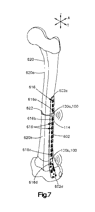
[0068] Turning now to Figs. 7 to 9, one example of an implantable sensor
system is
shown. The system comprises an anatomical implant 104 having an implant body
602 and at
least one implantable sensor 100. For example, the at least one implantable
sensor 100 can
include a first sensor 100a and a second sensor 100b. At least one, up to all,
of the at least one
implantable sensor 100 can be configured to be supported by the anatomical
implant body 602.
In this example, the anatomical implant 114 comprises a bone plate, and the at
least one sensor
16
CA 03072017 2020-02-03
WO 2019/032488 PCT/US2018/045477
100 is configured to track strain imparted by a bone 620 on the implant 114
during healing of the
bone 620. The bone 620 has a first portion 620a and a second portion 620b
separated by a
fracture 622 with respect to a longitudinal direction L. However, as described
above in relation
to Figs. 1 and 2, in alternative embodiments, the anatomical implant 114 could
be any suitable
anatomical implant and the sensor 100 could be any suitable sensor for
tracking any suitable
anatomical property.
[0069] The anatomical implant 114 has a body 602 having an anatomical-body-
facing
surface 602a and an outer surface 602b opposite the anatomical-body-facing
surface 602a along
a transverse direction T, perpendicular to the longitudinal direction L. In
this example, the
anatomical-body-facing surface 602a is a bone-facing surface. The anatomical
implant body 602
has a first end 602c and a second end 602d opposite the first end 602c. The
first and second ends
602c and 602d can be offset from one another along the longitudinal direction
L. Further, first
and second ends 602c and 602d can be offset from one another along a central
axis Ai of the
anatomical implant 114. Thus, in one embodiment, the central axis Ai can
extend substantially
along the longitudinal direction L; however, in alternative embodiments, the
central axis Ai can
be bent so as to not extend entirely along the longitudinal direction L. The
anatomical implant
body 602 has a first side 602e and a second side 602f that are offset from one
another along a
lateral direction A, perpendicular to both the longitudinal and transverse
directions.
[0070] The anatomical implant 114 is configured to be attached to a bone using
any
suitable attachment. For example, the implant 114 can include a plurality of
apertures
configured to receive bone screws therethrough to attach the implant 114 to
the bone. The
plurality of apertures 616 can include at least one pair of apertures spaced
from one another with
respect to the longitudinal direction L. For example, the at least one pair of
apertures can include
a first pair of apertures that includes a first aperture 616a and a second
aperture 616b spaced
from one another with respect to the longitudinal direction L. At least one
sensor 100a can be
disposed between the first and second apertures 616a and 616b. Accordingly,
the first and
second apertures 616a and 616b can receive bone screws therethrough so as to
secure a position
of the anatomical implant 114, and hence the at least one sensor 100a, with
respect to the
longitudinal direction L. In at least one embodiment, the plurality of
apertures 616 can include,
for each sensor 100 supported by the implant 114, at least one corresponding
pair of apertures
616, and each sensor 100 can be disposed between the apertures of its
corresponding pair of
apertures 616. Each sensor 100 can be disposed between the apertures of its
corresponding pair
of apertures 616 without any other sensors disposed between the corresponding
pair of apertures
616.
17
CA 03072017 2020-02-03
WO 2019/032488 PCT/US2018/045477
[0071] The anatomical implant 114 is configured to support at least one of the
sensors
100. For example, the anatomical implant body 602 can define at least one
recess 612 for each
sensor 100 supported by the implant body 602. The recess 612 can extend into
the outer surface
602b of the anatomical implant body 602 towards the inner surface 602a. The
recess 612 can be
configured to receive at least a portion of a corresponding one of the sensors
100 so as to at least
partially house the corresponding sensor 100. In alternative embodiments, one
or more of the
sensors 100 can be mounted to the outer surface 602b of the anatomical implant
602 without
being received in a recess such as the recess 612 or can be disposed inside
the anatomical
implant body 602 between the inner and outer surfaces 602a and 602b.
[0072] Each sensor 100 can comprise at least one sensing element 102, a
printed circuit
board 112, and an antenna 110 as shown in Fig. 9. Further, each of the at
least one sensor 100
can include a cover 610. It will be understood that sensors 100a and 100b can
each be
implemented as shown in Fig. 9. In one example, the at least one sensing
element 102 can be
part of a strain gauge having a substrate with first and second broadsides and
the at least one
sensing element in a manner similar to that described above in relation to
strain gauge 200 of
Fig. 3. The strain gauge can be supported by the anatomical implant body 602
such that the
second broadside of the strain gauge 200 is in contact with the anatomical
implant body 602.
Further, the strain gauge 200 can be supported such that the central axis As
of a first one of the
sensing elements 102a that extends along the first direction Di is aligned
with the longitudinal
direction L of the implant 114. Thus, the first sensing element 102a can be
configured so as to
detect tensile and compressive forces imparted by the first and second
portions 620a and 620b of
the bone 620 on the implant 114 along the longitudinal direction L. Further,
the strain gauge 200
can be supported such that the third direction D3 of the strain gauge 200 is
aligned with the
transverse direction T.
[0073] The at least one sensing element 102 can further include one or more
additional
sensing elements supported by the implant body 602 so as to detect one or both
of torsional and
bending forces imparted by the first and second portions 620a and 620b of the
bone 620 on the
implant 114. For example, the at least one sensing element 102 can include one
or more of the
sensing elements 102b and 102c of Fig. 3, which can be angularly offset from
the longitudinal
direction L so as to detect torsional and bending forces.
[0074] The printed circuit board 112 can include a substrate and one or more
integrated
circuits mounted onto the substrate. Further, the printed circuit board 112
can be configured as
described above in relation to printed circuit board 112. For example, the one
or more integrated
circuits can include an integrated circuit comprising the power device 106, an
integrated circuit
18
CA 03072017 2020-02-03
WO 2019/032488 PCT/US2018/045477
comprising the measurement device 104, and an integrated circuit comprising
the wireless
communicator 108. In at least one embodiment, the integrated circuit
comprising the power
device 106 can be implemented as an energy harvesting chip, the integrated
circuit comprising
the measurement device 104 can be implemented as a PicoStrain chip, and the
integrated
circuit comprising the wireless communicator 108 can be implemented as an RFID
chip.
100751 When each of the at least one sensor 100 is assembled, the at least one
sensing
element 102, the printed circuit board 112, and the antenna 110 can be aligned
along the
transverse direction T of the implant 114. The transverse direction T can be
aligned with third
direction D3 of the antenna and the strain gauge. For example, the printed
circuit board 112 can
be disposed between the at least one sensing element 102 and the antenna 110.
One of the first
and second broadsides of the at least one sensing element 102 (e.g., one of
the first and second
broadsides 202a and 202b of the strain gauge 200 of Fig. 3), can face towards
one of first and
second broadsides of the antenna 110 (e.g., one of first and second broadsides
504a and 504b of
Fig. 6). Similarly, one of first and second broadsides of the antenna 110
(e.g., one of first and
second broadsides 504a and 504b of Fig. 6) can face towards one of the first
and second
broadsides of the at least one sensing element 102 (e.g., one of the first and
second broadsides
202a and 202b of the strain gauge 200 of Fig. 3). Further, the printed circuit
board 112 can have
a first broadside that faces the at least one sensing element 102 and a second
broadside that is
opposite the first broadside along the transverse direction T and that faces
the antenna 110.
[0076] The cover 610 can be aligned with the at least one sensing element 102,
the
printed circuit board 112, and the antenna 110 along the transverse direction
T direction. Thus,
the antenna 110 can be disposed between the printed circuit board 112 and the
cover 610 with
respect to the select direction. The cover 610 can include an inner side and
outer side opposite
the inner side along the select direction. In at least one example, the inner
side can define a
recess that extends therein. Thus, the cover 610 can define a housing having a
recess configured
to house at least one of the at least one sensing element 102, the printed
circuit board 112, and
the antenna 110. Alternatively, the recess 612 in the implant body 602 can be
deeper so as to
receive an entirety of the sensor 100, and the inner side of the cover 610 can
be substantially
planar without a recess so as to cover the recess 612. The cover can be made
from any suitable
material. For example, the cover 610 can be made from a biocompatible
material, including
(without limitation) a biocompatible polymer such as polyether ether ketone
(PEEK), a metal, or
ceramic. In the assembled configuration, each sensor 100 can have an overall
size in a plane
perpendicular to the select direction between approximately 8 mm x 8 mm and
approximately 20
mm x 20 mm, and increments of 1 mm therebetween. In one example, each sensor
100 can have
19
CA 03072017 2020-02-03
WO 2019/032488 PCT/US2018/045477
an overall size in the plane of approximately 12 mm x 12 mm. Each sensor 100
can further have
an overall thickness in the select direction between approximately 2 mm and 4
mm.
100771 Turning now to Figs. 1, 2, 3, 4 and 10, a method of detecting a value
of an
anatomical property of a patient from the at least one sensor 100 of Fig. 2
implanted into a
patient's body is now described. In step 702, the at least one capacitor 302
of the at least one
sensor 100 is charged to a reference voltage. For example, the power device
106 can provide
power to the at least one capacitor 302. The charging step 702 can comprise
capturing energy
from a source separate from the at least one sensor 100 at an energy-
harvesting device, and
providing the energy from the source to the at least one capacitor 302 so as
to charge the at least
one capacitor 302. The energy source can be radio waves from the reader 116
that excite the
antenna coil of the antenna 100 to produce a current in the antenna coil. For
example, in the case
of RFID, the antenna 110 can receive power from the radio-frequency signal
transmitted by the
reader 116. In alternative embodiments, the energy source can include (without
limitation)
kinetic energy, electric fields, magnetic fields, and so on. Alternatively or
additionally, the
power device 106 can provide power to the at least one capacitor 302 from a
battery of the power
device 106.
[0078] In step 704, the at least one capacitor 302 is discharged through at
least one
resistive sensing element of the at least one sensor 102. In some embodiments,
the discharging
step 804 can comprise discharging the at least one capacitor 302 through at
least two resistive
sensing elements that are non-parallel to one another such as sensing elements
102a and 102b of
Fig. 3. Further, in some embodiments, the discharging step 704 can comprise
discharging the at
least one 302 capacitor through three resistive sensing elements that are non-
parallel to one
another such as sensing elements 102a, 102b, and 102c of Fig. 3.
[0079] In step 706, at least one measurement value is generated that is
proportional to
the value of the anatomical property. The generating step 706 comprises
measuring a discharge
time of the at least one capacitor 302 to a trigger voltage. In at least some
embodiments, the
generating step 706 can comprise measuring the discharge time of the at least
one capacitor 302
using a time-to-digital converter 304. Further, the generating step 706 can
comprise calculating
the measurement value based on the discharge time. However, in some
embodiments, the
measurement value can be the discharge time. Steps 704 and 706 can be
performed for each
sensing element in a sequential manner. For example, the at least one
capacitor 302 can be
discharged through a first one of the sensor elements 102a, 102b, and 102c to
generate a first
measurement value, then a second one of the sensor elements 102a, 102b, and
102c to generate a
CA 03072017 2020-02-03
WO 2019/032488 PCT/US2018/045477
second measurement value, and finally through a third one of the sensor
elements 102a, 102b,
and 102c to generate a third measurement value.
[0080] In step 708, the at least one measurement value is wirelessly
communicated
through skin of the patient to an external wireless communicator situated
outside of the patient's
body. The wireless communication step 708 can comprise wirelessly
communicating the at least
one measurement value to the external wireless communicator. Further, the
wireless
communicating step 708 can comprise communicating a unique ID to the external
wireless
communicator that identifies the at least one sensor. In the case of RFID, the
electronics
connected to the antenna 110 can modulate the load seen by the antenna 110
based on the at least
one measurement value and optionally the unique ID, and this modulation can be
sensed by the
reader 116.
[0081] Embodiments of the disclosure can further include implants, systems,
and
methods including at least two sensors. For example, according to various
embodiments, the
sensors of the present disclosure can be used to implement any of the sensors
of U.S. patent
application publication 2013/0190654, the teachings of which are hereby
incorporated by
reference as if set forth in their entirety herein. U.S. patent application
publication
2013/0190654 discloses systems including at least two sensors. In general, a
first sensor is
supported at the fracture site in the bone to measure strain and/or load at
the fracture site when
the bone is under a given load. As the bone heals, the bone increasingly
shares any load
imparted by the patient's body on the implant. Thus, the strain or loading
imposed on the
implant at the first sensor is affected by the strength or stiffness of the
weakened bone portion at
the fracture. In theory, if the bone were under a constant load, then the load
imparted on the
bone would increase as the bone heals, while the load imparted on the implant
at the first sensor
would decrease.
[0082] However, the load imparted on the implant might not be constant. Rather
the
load might vary based on, for example, the amount of load that the patient
places on the bone
(e.g., the amount of weight that a patient places on a leg). Therefore, a
second sensor can be
supported at the healthy (i.e., non-damaged) bone to detect the amount of
strain or loading that
should be experienced by healthy bone when the bone is under the given load.
The measured
strain or loading from the first sensor at the damaged portion of the bone can
then be compared
to the measured strain or loading from the second sensor at the healthy
portion of the bone.
[0083] For example, and with reference to Figs. 7 and 8, the at least one
sensor 100 can
include a first sensor 100a configured to be supported by the implant body 602
and a second
sensor 100b configured to be supported by the implant body 602. Each sensor
100a and 100b
21
CA 03072017 2020-02-03
WO 2019/032488 PCT/US2018/045477
can include a unique ID to distinguish the sensors 100a and 100b from one
another. Thus, the
first sensor 100a can include a first unique ID, and the second sensor 100b
can include a second
unique ID, different from the first unique ID. The unique IDs can also be used
to distinguish the
sensors 100a and 100b from sensors implanted in other patients. The unique IDs
can be IDs of
RFID tags.
[0084] The first and second sensors 100a and 100b can be spaced from one
another
with respect to the longitudinal direction L. The first sensor 100a can be
configured to be
supported by the implant body 602 such that, when the implant 114 is attached
to the bone 100,
the first sensor 100a is disposed adjacent to or over the fracture 622. For
example, the first
sensor 100a can be aligned with the fracture 622 with respect to the
transverse direction T. The
first sensor 100a can also be disposed between first and second apertures 616a
and 616b that are
configured to receive a bone screw therethrough to attach the implant 114 to
bone. Thus, the
first sensor 100a can be isolated between the first and second apertures 616a
and 616b.
[0085] The second sensor 100b can be supported by the implant body 602 such
that the
second sensor 100b is supported over a healthy (e.g., solid) portion 620b of
the bone 620. For
example, the second sensor 100b can be aligned with the healthy portion 620b
with respect to the
transverse direction T. The second sensor 100b can also be disposed between
first and second
apertures 616c and 616d that are configured to receive a bone screw
therethrough to attach the
implant 114 to bone. Thus, the second sensor 100b can be isolated between the
first and second
apertures 616c and 616d. The first and second apertures 616a and 616b
corresponding to the
first sensor 100a can each be spaced from the first and second apertures 616c
and 616d
corresponding to the second sensor 100b with respect to the longitudinal
direction L.
Alternatively, one of the apertures 616b and 616c can be shared between the
first and second
sensors 100a and 100b.
[0086] It will be understood that, as an alternative, loading on the healthy
portion 620b
of the bone can be detected without the second sensor 100b being supported by
the implant 114.
For example, as shown in Fig. 11, the loading on the healthy portion 620b can
also be detected
by attaching the second sensor 100b directly onto the bone 620. As another
example, the loading
of the healthy portion 620b can be detected by attaching the second sensor
100b to another
implant that is in turn attached to the bone 620. The other implant can
include, for example,
another bone plate, a bone anchor such as a screw, and so on. Thus, according
to some
alternative embodiments, the system can comprise a first sensor 100a supported
by the implant
body 602 and a second sensor 100b configured to be attached to the bone 620 so
as to be spaced
from and separate from the implant 114.
22
CA 03072017 2020-02-03
WO 2019/032488 PCT/US2018/045477
[0087] A method of operating the system of Figs. 7 and 11 can include
performing the
method of Fig. 10 for each of the first and second sensors to (i) generate a
first measurement
value for the first sensor 100a and a second measurement value for the second
sensor 100b, and
(ii) communicate the first measurement value with the first unique ID and the
second
measurement value with the second unique ID to the external wireless
communication device.
The method can further include a step of generating a comparison value based
on the first and
second measurement values. In one example, the comparison value can be a ratio
of one of the
first and second measurement values to the other of the first and second
measurement values. In
another example, the comparison value can be a difference between the first
and second
measurement values. In yet another example, the comparison can be determined
in a look-up
table by looking up the first and second measurement values and finding the
comparison therein
that corresponds to the first and second measurement values.
[0088] Referring back to Figs. 1 and 9, the current of the reader 116 can
cause eddy
currents in a metallic implant 114. Moreover, as the radio waves excite the
antenna coil of the
antenna 110 to produce a current in the antenna coil, the antenna coil
produces an
electromagnetic field that can also excite eddy currents in the metallic
implant 114. The eddy
currents in turn can decrease the magnetic flux observed by the antenna coil
of the antenna 110.
Moreover, the eddy currents can rotate in direction opposite the current flow
in the antenna coil,
thereby opposing the current in the antenna coil of the antenna 110 and
changing the tuning
frequency of the antenna coil. This interference from the eddy currents can
reduce the efficiency
of the wireless link between the reader 116 and the sensor 100.
[0089] To limit the effect of eddy currents, a ferrite layer (not shown) can
be
implemented between the antenna 110 and the implant 114. The ferrite layer can
prevent at least
some of the electro-magnetic field from reaching the metallic implant 114,
thus limiting the eddy
currents that are excited in the metallic implant 114. However, ferrite is not
biologically
compatible, and therefore, presents some challenges when being implemented in
an implantable
sensor.
[0090] As an alternative to ferrite, and with reference to Figs. 12 and 13,
the sensor 100
can comprise a shield 124 disposed between the antenna 110 and the implant
114. The shield
124 can have at least one inductive shield coil 802 and a substrate 804 that
supports the shield
coil 802. The antenna system 109 of Fig. 2 can comprise the antenna 110 and
the shield 124.
Further, the shield coil 802 can be connected in series with the at least one
antenna coil 502. The
shield can be configured to limit magnetic flux passing through the shield 124
or even
substantially prevent magnetic flux from passing through the shield 124
altogether. As an
23
CA 03072017 2020-02-03
WO 2019/032488 PCT/US2018/045477
electrical current flows in the shield coil 124, the current can mimic the
eddy currents in the
implant. Consequently, the shield 124 can limit the amount in which the
implant 114 beneath the
shield 124 is exposed to the magnetic field generated by the antenna 110, or
prevent such
exposure altogether. In other words, the magnetic field of the shield 124 can
cancel a portion of
the magnetic field of the antenna 110 that would otherwise extend below the
shield 124.
Reducing the interaction between the antenna 110 and the implant 114 can
result in better
performance of the antenna 110 such as a longer wireless communication range
between the
antenna and the reader 116 and more reliable tuning.
[0091] The substrate 804 can be a film or other suitable substrate. In one
example, the
shield 124 can be implemented as a flexible printed circuit board. The
substrate 804 can have a
first broadside 804a and a second broadside 804b opposite the first broadside
804a. The
substrate 804 can further have a first edge 804c and a second edge 804d
opposite one another
with respect to a first direction DAL The substrate 804 can yet further have a
third edge 804e and
a fourth edge 804f opposite one another with respect to the second direction
DA2, perpendicular
to the first direction DAL The first and second broadsides 804a and 804b can
extend between the
first and second edges 804c and 804d and between the third and fourth edges
804e and 804f
The first broadside 804a can be planar along the first and second directions
DA1 and DA2.
Similarly, the second broadside 804b can be planar along the first and second
directions DA1 and
DA2. The first and second broadsides 804a and 804b can be opposite one another
with respect to
a third direction DA3, perpendicular to both the first and second directions
DA1 and DA2. Note
that the directions DA1, DA2, and DA3 can be aligned with the directions Di,
D2, and D3 of the at
least one sensing element 102 of Fig. 3, or can be angularly offset from the
directions Di, D2, and
D3.
[0092] The substrate 804 can have a height from the first edge 804c to the
second edge
804d with respect to the first direction DAL The substrate 804 can further
define a width from
the third edge 804e to the fourth edge 804f with respect to the second
direction DA2. The
substrate 804 can yet further define a thickness from the first broadside 804a
to the second
broadside 804b with respect to the third direction DA3. The height and width
can be greater than
the thickness. In some examples, the substrate 804 can have a rectangular
shape; however, in
alternative examples, the substrate 804 can have any other suitable shape.
[0093] The shield coil 802 can be an electrically conductive wire or trace.
The shield
coil 802 can include a first end 802a and a second end 802b offset from one
another. The coil
802 can extend about a center of the coil 802 in a spiral pattern from the
first end 802a to the
second end 802b such that the second end 802b is spaced closer to the center
of the coil 802 than
24
CA 03072017 2020-02-03
WO 2019/032488 PCT/US2018/045477
the first end 802a. Thus, the coil 802 can have a plurality of turns. The
number of turns can be
less than or equal to the total number of turns of the at least one antenna
coil 502. The coil 802
can have an overall shape that is substantially square; however, in
alternative embodiments, the
coil 802 can have another suitable shape.
[0094] The antenna 110 and shield 124 can extend along respective planes. When
the
sensor is assembled, the shield 110 can be disposed below the antenna 124 such
that the plane of
the antenna 110 is spaced from the plane of the shield 124 along the third
direction DA3. Thus,
the plane of the antenna 110 can face the plane of the shield 124 along the
third direction DA3 In
some embodiments, the respective planes can be substantially parallel to one
another, although
the respective planes can be offset by another angle such as by less than 30
degrees. One of the
broadsides 504a and 504b of the antenna 110 can face one of the broadsides
804a and 804b of
the shield 124. Further, the antenna 110 and the shield 124 can define a space
between their
respective planes with respect to the third direction DA3.
[0095] In some preferred examples, the shield coil 802 can be configured to
carry
current in a direction that is opposite that of the antenna coil 502. For
example, each of the at
least one antenna coil 502 can be wound in a first direction, and the shield
coil 802 can be wound
in a second direction, opposite from the first direction when the shield coil
802 is disposed below
the at least one antenna coil 502. More specifically, the at least one antenna
coil 502 can be
wound in one of a clockwise and a counterclockwise direction, beginning from
an interior of the
antenna coil 502, as viewed in a direction towards the implant 114, while the
shield coil 802 can
be wound in the other one of the clockwise and counterclockwise direction,
beginning from an
interior of the shield coil 802, as viewed in the direction towards the
implant 114. Thus, the
shield coil 802 can be configured to generate a magnetic field in a direction
that opposes the
magnetic field of the at least one antenna coil 502. Further, in some
preferred embodiments, the
shield coil 802 can have a number of turns that is less than a total number of
turns of the at least
one antenna coil 502. In some such examples, the shield coil 802 can have
approximately half
the number of turns of the at least one antenna coil 502. Thus, the shield
coil 802 can produce a
weaker magnetic field that opposes the magnetic field of the at least one
antenna coil 502.
[0096] Referring to Fig. 14, in some embodiments, the antenna system 109 can
include
the antenna coil 502, the shield coil 802, and a substrate 904, where both the
antenna coil 502
and shield coil 802 are supported by the substrate 904. Thus, the antenna 110
can include the
antenna coil 502 and a first portion 908 of the substrate 904, and the shield
124 can include the
shield coil 802 and a second portion 910 of the substrate 904. The antenna
system 109 is
configured to be bent between an unstacked configuration as shown in Fig. 13
and a stacked
CA 03072017 2020-02-03
WO 2019/032488 PCT/US2018/045477
configuration (not shown). In the unstacked configuration, the antenna coil
502 and the shield
coil 802 are spaced from one another along the second direction DA2. Thus, the
antenna coil 502
and the shield coils 802 are disposed side-by-side. In the stacked
configuration, the substrate
904 is bent about an axis A that extends between the antenna coil 502 and the
shield coil 802
along the first direction DA1 such that the antenna coil 502 and the shield
coil 802 are spaced
from one another along the third direction DA3, which is perpendicular to both
the first and
second directions DA1 and DA2. The antenna coil 502 and shield coil 802 can be
wound in the
same direction (i.e., clockwise or counterclockwise) when the antenna system
109 is in the
unstacked configuration, and can be wound in opposite directions when the
antenna system 109
is bent to the stacked configuration.
[0097] The substrate 904 can be a film or other suitable substrate. In one
example, the
assembly can be implemented as a flexible printed circuit board. The substrate
904 can have a
first broadside 904a and a second broadside 904b opposite the first broadside
904a. The
substrate 904 can further have a first edge 904c and a second edge 904d
opposite one another
with respect to a first direction DAL The substrate 904 can yet further have a
third edge 904e and
a fourth edge 904f. The third edge 904e and fourth edge 904f can be spaced
opposite one
another with respect to the second direction DA2 when the substrate 904 is in
the unstacked
configuration. The first and second broadsides 904a and 904b can extend
between the first and
second edges 904c and 904d and between the third and fourth edges 904e and
904f The first
broadside 904a can be planar along the first and second directions DA1 and DA2
when the
substrate is in the unstacked configuration. Similarly, the second broadside
904b can be planar
along the first and second directions DA1 and DA2 when the substrate is in the
unstacked
configuration.
[0098] The substrate 904 can have a height from the first edge 904c to the
second edge
904d with respect to the first direction DAL The substrate 904 can further
define a width from
the third edge 904e to the fourth edge 904f with respect to the second
direction DA2. The
substrate 904 can yet further define a thickness from the first broadside 904a
to the second
broadside 904b with respect to the third direction DA3. The height and width
can be greater than
the thickness. In some examples, the substrate 904 can have a rectangular
shape; however, in
alternative examples, the substrate 904 can have any other suitable shape.
[0099] The antenna 110 and shield 124 can define respective planes. In the
unstacked
configuration, the respective planes can be substantially in-line with one
another. The substrate
904 can include a flexible bend region 906 between the antenna 110 and the
shield 124. The
substrate 904 can be configured to bend at the bend region 906 so as to
transition the antenna
26
CA 03072017 2020-02-03
WO 2019/032488 PCT/US2018/045477
system 109 between the unstacked configuration and the stacked configuration.
In the stacked
configuration, the plane defined by the antenna 110 is spaced from the plane
defined by the
shield 124 along the third direction DA3. Thus, the plane defined by the
antenna 110 can face the
plane defined by the shield 124 along the third direction DA3. For example,
the antenna system
109 can be bent such that one of the first and second broadsides 904a and 904b
at the first
portion 908 of the substrate 904 (e.g., at the antenna coil 502) faces the one
of the first and
second broadsides 904a and 904b at the second potion 910 of the substrate 904
(e.g., at the shield
coil 802).
[00100] In the stacked configuration, the plane defined by the antenna 110 can
be
disposed above the plane defined by the shield 124 with respect to the third
direction DA3. The
respective planes can be substantially parallel to one another, although the
respective planes can
be offset by another angle such as by less than 30 degrees. Further, the
antenna system can
define a space between the planes that define the antenna 110 and the shield
124 with respect to
the third direction DA3 when the antenna system 109 is in the stacked
configuration. At least
one, up to all, of the electrical components 107 can be disposed in the space
between the antenna
110 and the shield 124 as discussed above in relation to Fig. 13.
[00101] Turning now to Figs. 15 and 16, two exemplary stack-ups of the
components
of the sensor 100 are shown. In these particular examples, the antenna 110 is
illustrated with two
antenna coils 502(1) and 502(2), and the coils are shifted relative to one
another such that the
turns of the antenna coil 502(2) are disposed below the gaps between the turns
of the antenna
coil 502(1). It will be understood that, in alternative embodiments, the
antenna 110 can include
only one antenna coil 502(1) or 502(2), or the coils can be aligned, rather
than shifted, such that
the turns of the antenna coils 502(1) and 502(2) are aligned along the
transverse direction T. In a
similar manner, the shield 124 can have more than one shield coil disposed
over one another or
can have only one shield coil.
[00102] The shield 124 can be disposed below the antenna 110. For example, the
shield 124 can be disposed between the antenna 110 and the implant 114 when
the sensor 100 is
attached to the implant 114. In at least some embodiments, the shield 124 can
be disposed
between the antenna 110 and the at least one sensing element 102. In some such
embodiments as
shown in Fig. 15, the shield 124 can be disposed between the at least one
sensing element 102
and at least one of the electrical components 107 such as at least one, up to
all of, the
measurement device 104, the power device 106, and the wireless communicator
108. Thus, the
electrical components 107 can be disposed in the space between the shield 124
and the antenna
110. Note that the components 107 are illustrated schematically in Figs. 15
and 16, and the
27
CA 03072017 2020-02-03
WO 2019/032488 PCT/US2018/045477
particular orientation of the components 107 on the printed circuit board 112
can vary from the
orientation shown. Further, the sensor 100 can include various spacers between
adjacent layers
of the sensor 100, such as spacers 126 and 128. In alternative embodiments as
shown in Fig. 16,
the electrical components 107 can be disposed below the shield 124. Thus, the
shield 124 can be
disposed between the antenna 110 and the electrical components 107 such as the
measurement
device 104, the power device 106, and the wireless communicator 108.
[00103] Turning now to Fig. 17, an electrical circuit diagram of one example
of the
antenna system 109 of Fig. 2 is shown. The antenna system 109 comprises the
antenna 110 and
the shield 124 connected in series with one another. In this example, the
antenna 110 comprises
the first inductive antenna coil 502(1) and the second inductive antenna coil
502(2) connected in
series with one another, although in alternative embodiments, the antenna 110
can comprise just
one inductive antenna coil or more than two inductive coils with capacitors
placed between
adjacent pairs of the inductive coils. Further, the shield 124 includes one
inductive coil 802,
although it will be understood that the shield 124 can similarly include more
than one inductive
coil. The antenna system 109 can comprise at least one, such as a plurality
of, capacitors 1002,
1004, 1006. A capacitor 1002 can be connected between the first and second
antenna coils
502(1) and 502(2). The capacitor 1002 can cause the self-resonance of the
first and second
antenna coils 502(1) and 502(2) to be higher, which in turn can decrease
losses in the coils
502(1) and 502(2). A capacitor 1004 can be connected in series between the
antenna 110 and the
electrical components of the sensor 100 such as at least one, up to all of,
the measurement device
104, the power device 106, and the wireless communicator 108 of Fig. 2. A
capacitor 1006 can
be connected in series between the shield 124 and the electrical components of
the sensor 100
such as at least one, up to all of, the measurement device 104, the power
device 106, and the
wireless communicator 108 of Fig. 2. It will be understood that, in
alternative embodiments, one
or more parallel capacitors can be used. For example, an optional parallel
capacitor 1010 can be
connected as shown in dashed lines. In some embodiments, the capacitor 1004
can have a
capacitance that is equal to a capacitance of the capacitor 1006. The antenna
system 109 can be
tuned before being implanted onto the metallic implant. The antenna 110 and
shield 124 can be
tuned together since they are connected in series. After mounting on the
sensor 100 onto the
metallic implant, the antenna system 109 can maintain its tuning.
[00104] Turning to Figs. 18 and 19, magnetic and electric fields of the sensor
100 are
shown, respectively, where the darker shading indicates areas where the
magnetic and electric
fields have greater intensity and the lighter shading indicates areas where
the magnetic and
electric fields have lower intensity. As shown in Fig. 18, the shield 124
generates its own
28
CA 03072017 2020-02-03
WO 2019/032488 PCT/US2018/045477
magnetic field when current flows through the shield coil 802. The magnetic
field of the shield
124 limits the magnetic flux of the antenna 110 from passing through the
shield 124 or prevents
the magnetic flux of the antenna 110 from passing through the shield 124
altogether. As shown
in Fig. 19, the shield 124 limits the electric field below the shield 124. As
a result, the electric
field of the antenna 110 does not excite eddy currents, or excites only low
magnitude eddy
currents, in the implant below the shield 124. Moreover, as shown in Fig. 19,
there is a region
1000 defined between the antenna 110 and the shield 124 in which the electric
field is relatively
low in comparison to the electric field adjacent to the at least one antenna
coil 502. The region
1000 is defined in an area that extends from the shield 124 and upwards
towards the antenna 110.
The region 1000 has a first height directly below the at least one antenna
coil 502, and a second
height directly below a center of the at least one antenna coil 502 that is
greater than the first
height. Thus, it can be understood that metallic objects, such as the
electrical components 107
and/or the ground plane of the printed circuit board 112, can be positioned in
the region 1000
without significantly hurting the performance of the antenna 110.
[00105] It will be appreciated by those skilled in the art that changes could
be made to
the embodiments described above without departing from the broad inventive
concept thereof
Furthermore, it should be appreciated that the structure, features, and
methods as described
above with respect to any of the embodiments described herein can be
incorporated into any of
the other embodiments described herein unless otherwise indicated. It is
understood, therefore,
that this invention is not limited to the particular embodiments disclosed,
but it is intended to
cover modifications within the spirit and scope of the present disclosure.
Further, it should be
appreciated, that the term substantially indicates that certain directional
components are not
absolutely perpendicular to each other and that substantially perpendicular
means that the
direction has a primary directional component that is perpendicular to another
direction.
[00106] Embodiments of the disclosure will be understood with reference to the
following examples:
[00107] Example 1: A sensor configured to be implanted into a patient, the
sensor
comprising:
at least one sensing element;
a measurement device in communication with the at least one sensing element,
the measurement device including at least one capacitor and configured to
measure a discharge
time of the at least one capacitor through the at least one sensing element so
as to generate a
measurement value that is proportional to a value of an anatomical property of
the patient
observed by the sensor.
29
CA 03072017 2020-02-03
WO 2019/032488 PCT/US2018/045477
[00108] Example 2: The sensor of example 1, wherein the at least one sensing
element
comprises a resistor, and the measurement device is configured to measure the
discharge time of
the at least one capacitor through the resistor so as to generate the
measurement value.
[00109] Example 3: The sensor of any one of the preceding examples, comprising
an
internal wireless communicator in communication with the measurement device,
the wireless
communicator configured to wirelessly communicate the measurement value
through skin of the
patient to an external wireless communicator situated outside of the patient's
body.
[00110] Example 4: The sensor of any one of the preceding examples, wherein
the
measurement device comprises a time-to-digital converter configured to measure
discharge time
of the capacitor through the at least one sensing element.
[00111] Example 5: The sensor of example 4, wherein the measurement device
comprises a clock, and the time-to-digital converter is configured to
increment in response to a
clock signal of the clock.
[00112] Example 6: The sensor of any of the preceding examples, wherein the
sensor
comprises a strain gauge that includes the at least one sensing element.
[00113] Example 7: The sensor of example 6, wherein the strain gauge includes
a
substrate that carries the at least one sensing element, and the at least one
sensing element
includes first and second sensing elements, wherein the first and second
sensing elements are
non-parallel to one another.
[00114] Example 8: The sensor of example 7, wherein the at least one sensing
element
includes a third sensing element, wherein the third sensing element is non-
parallel to the first and
second sensing elements.
[00115] Example 9: The sensor of example 8, wherein each of the first, second,
and
third sensing elements includes a longitudinal axis, and the longitudinal axes
of the first, second,
and third sensing elements intersect one another.
[00116] Example 10: The sensor of any one of the preceding examples, wherein
the at
least one sensing element comprises a semiconductor bar-type strain gauge.
[00117] Example 11: The sensor of example 3, wherein the internal wireless
communicator comprises a wireless transmitter, and the sensor comprises an
antenna.
[00118] Example 12: The sensor of example 11, wherein the wireless transmitter
is
configured to communicate using radio-frequency identification (RFID).
[00119] Example 13: The sensor of any one of the preceding examples,
comprising a
power device configured to supply power to the measurement device.
CA 03072017 2020-02-03
WO 2019/032488 PCT/US2018/045477
[00120] Example 14: The sensor of example 13, wherein the power device
includes an
energy harvesting device.
[00121] Example 15: The sensor of example 14, wherein the energy harvesting
device
is configured to capture energy from radio waves communicated to the sensor.
[00122] Example 16: A system comprising:
a first sensor configured as recited in any one of the preceding claims; and
an anatomical implant configured to support the sensor.
[00123] Example 17: The system of example 16, comprising a second sensor
configured as recited in any one of the preceding claims.
[00124] Example 18: The system of example 17, wherein the first sensor is
configured
to be supported by the anatomical implant such that the first sensor is
aligned with a bone
fracture and the second sensor is configured to be supported such that the
second sensor is
aligned with a portion of healthy bone.
[00125] Example 19: The system of example 17, wherein the first sensor
includes a
first unique identifier, and the second sensor includes a second unique
identifier, different from
the first unique identifier.
[00126] Example 20: A method of detecting a value of an anatomical property of
a
patient from at least one sensor implanted into a patient's body, the method
comprising steps of:
charging at least one capacitor of the at least one sensor to a reference
voltage;
discharging the at least one capacitor through at least one sensing element of
the at least
one sensor; and
generating a measurement value that is proportional to the value of the
anatomical
property, the generating step comprising measuring a discharge time of the at
least one
capacitor to a trigger voltage.
[00127] Example 21: The method of example 20, wherein discharging step
comprises
discharging the at least one capacitor through at least one resistor of the at
least one resistive
sensing element.
[00128] Example 22: The method of any one of examples 20 and 21, further
comprising wirelessly communicating the measurement value through skin of the
patient to an
external wireless communicator situated outside of the patient's body.
[00129] Example 23: The method of any one of examples 20 to 22, wherein the
charging step comprises a power device providing power to the at least one
capacitor.
[00130] Example 24: The method of example 23, wherein the charging step
comprises
capturing energy from a source separate from the at least one sensor at an
energy-harvesting
31
CA 03072017 2020-02-03
WO 2019/032488 PCT/US2018/045477
device, and providing the energy from the source to the at least one capacitor
so as to charge the
at least one capacitor.
[00131] Example 25: The method of example 24, wherein the source is radio
waves.
[00132] Example 26: The method of any one of examples 20 to 25, wherein the
generating step comprises measuring the discharge time of the at least one
capacitor using a
time-to-digital converter.
[00133] Example 27: The method of any one of examples 20 to 26, wherein the
generating step comprises calculating the measurement value based on the
discharge time.
[00134] Example 28: The method of any one of examples 20 to 27, wherein the
measurement value is the discharge time.
[00135] Example 29: The method of any one of examples 20 to 28, wherein the
discharging step comprises discharging the at least one capacitor through at
least two resistive
sensing elements that are non-parallel to one another.
[00136] Example 30: The method of any one of examples 20 to 29, wherein the
discharging step comprises discharging the at least one capacitor through
three resistive sensing
elements that are non-parallel to one another.
[00137] Example 31: The method of any one of examples 20 to 30, wherein the
wirelessly communicating step comprises communicating the measurement value to
the external
wireless communicator using radio frequency identification (RFID).
[00138] Example 32: The method of any one of examples 20 to 31, wherein the
wirelessly communicating step comprises communicating a unique identifier to
the external
wireless communicator that identifies the at least one sensor.
[00139] Example 33: The method of any one of examples 20 to 32, wherein the
measurement value is proportional to strain on the at least one sensor.
[00140] Example 34 The method of any one of examples 20 to 33, wherein:
the at least one sensor comprises a first sensor aligned with a bone fracture
and a
second sensor aligned with healthy bone; and
the method comprises:
performing the charging, discharging, generating, and wirelessly
communicating steps for the first sensor to generate a first measurement value
and for the second
sensor to generate a second measurement value; and
generating a comparison value based on the first and second measurement
values.
32
CA 03072017 2020-02-03
WO 2019/032488 PCT/US2018/045477
[00141] Example 35: A sensor configured to be implanted into a patient, the
sensor
comprising:
a semiconductor strain gauge having a substrate and first, second, and third
sensing elements arranged on the substrate such that the first, second, and
third sensing elements
are non-parallel to one another; and
a measurement device in communication with the first to third sensing
elements,
the measurement device configured to generate a measurement value that is
proportional to a
value of an anatomical property of the patient observed by the sensor.
[00142] Example 36: The sensor of example 35, comprising an internal wireless
communicator in communication with the measurement device, the wireless
communicator
configured to wirelessly communicate the measurement value through the skin of
the patient to
an external wireless communicator situated outside of the patient's body.
[00143] Example 37: The sensor of example 35, wherein the internal wireless
communicator comprises a wireless transmitter, and the sensor includes an
antenna.
[00144] Example 38: The sensor of example 37, wherein the sensor comprises a
printed
circuit board that includes a substrate, and each of the measurement device
and the wireless
transmitter is implemented as an integrated circuit that is mounted onto the
substrate.
[00145] Example 39: The sensor of example 38, wherein the printed circuit
board is
disposed between the semiconductor strain gauge and the antenna.
[00146] Example 40: The sensor of example 35, comprising a cover that
configured to
be disposed over the semiconductor strain gauge, the measurement device, and
the antenna such
that the antenna is disposed between the semiconductor strain gauge and the
cover.
[00147] Example 41: The sensor of any one of examples 35 to 40, wherein the
measurement device includes at least one capacitor and is configured measure a
discharge time
of the at least one capacitor through the first to third sensing elements so
as to generate the
measurement value.
[00148] Example 42: The sensor of example 41, wherein the measurement device
comprises a time-to-digital converter configured to measure the discharge
time.
[00149] Example 43: A system comprising:
an anatomical implant configured to be implanted into a patient;
a first sensor supported by the anatomical implant, and a second sensor, each
of
the first and second sensors comprising:
at least one sensing element;
33
CA 03072017 2020-02-03
WO 2019/032488 PCT/US2018/045477
a measurement device in communication with the at least one sensing element,
the measurement device configured to generate a measurement value that is
proportional to a
value of an anatomical property of the patient; and
an internal wireless communicator configured to wirelessly communicate the
measurement value and a unique identifier through skin of the patient to an
external wireless
communicator situated outside of the patient, wherein the unique identifier of
the first sensor is
different from the unique identifier of the second sensor.
[00150] Example 44: The system of example 43, wherein:
the at least one sensing element of each of the first and second sensors
comprises
a resistor; and
the measurement device of each of the first and second sensors comprises a
capacitor and is configured to measure a discharge time of the capacitor
through a corresponding
one of the resistors so as to generate a corresponding one of the measurement
values.
[00151] Example 45: The system of example 44, wherein each of the first and
second
measurement devices comprises a time-to-digital converter configured to
measure the discharge
time of a corresponding one of the capacitors through a corresponding at least
one sensing
element.
[00152] Example 46: The system of any one of examples 43 to 45, wherein each
internal wireless communicator comprises a radio frequency identification
(RFID)
communicator.
[00153] Example 47: The system of any one of examples 43 to 46, wherein each
of the
measurement devices comprises a clock, and the time-to-digital converter of
each measurement
device is configured to increment in response to a clock signal of a
corresponding one of the
clocks.
[00154] Example 48: The system of any of examples 43 to 47, wherein each of
the first
and second sensors comprises a strain gauge that includes a corresponding at
least one sensing
element.
[00155] Example 49: The system of example 48, wherein each strain gauge
includes a
substrate that carries a corresponding at least one sensing element, and the
corresponding at least
one sensing element includes first and second sensing elements, wherein the
first and second
sensing elements are non-parallel to one another.
[00156] Example 50: The system of example 49, wherein the at least one sensing
element includes a third sensing element, wherein the third sensing element is
non-parallel to the
first and second sensing elements.
34
CA 03072017 2020-02-03
WO 2019/032488 PCT/US2018/045477
[00157] Example 51: The system of example 50, wherein each of the first,
second, and
third sensing elements includes a longitudinal axis, and the longitudinal axes
of the first, second,
and third sensing elements intersect one another.
[00158] Example 52: The system of any one of examples 43 to 51, wherein each
sensing element comprises a semiconductor bar-type strain gauge.
[00159] Example 53: The system of any one of examples 43 to 52, wherein each
internal wireless communicator comprises a wireless transmitter, and the
sensor comprises an
antenna.
[00160] Example 54: The system of example 53, wherein each wireless
transmitter is
configured to communicate using radio-frequency identification (RFID).
[00161] Example 55: The system of any one of examples 43 to 54, wherein each
sensor
comprises a power device configured to supply power to the measurement device.
[00162] Example 56: The system of example 55, wherein each power device
includes
an energy harvesting device.
[00163] Example 57: The system of example 56, wherein each energy harvesting
device is configured to capture energy from radio waves communicated to the
energy harvesting
device.
[00164] Example 58: A sensor configured to be implanted into a patient, the
sensor
comprising:
at least one sensing element;
a measurement device in communication with the at least one sensing element,
the measurement device configured to generate a measurement value that is
proportional to a
value of an anatomical property of the patient observed by the sensor;
an antenna having at least one inductive antenna coil that is wound in a first
direction, the antenna coil configured to wirelessly transmit the measurement
value to a reader
outside of the patient; and
a shield disposed below the antenna, the shield having at least one inductive
shield coil that is connected in series with the antenna coil and is wound in
a second direction,
opposite the first direction.
[00165] Example 59: The sensor of example 58, wherein the shield is configured
to
limit magnetic flux passing through the shield.
[00166] Example 60: The sensor of any one of examples 58 and 59, wherein the
shield
coil has a number of turns that is less than a number of turns of the antenna
coil.
CA 03072017 2020-02-03
WO 2019/032488 PCT/US2018/045477
[00167] Example 61: The sensor of anyone of examples 58 to 60, wherein the
shield
coils has a number of turns that is equal to a number of turns of the at least
one inductive antenna
coil.
[00168] Example 62: The sensor of any one of examples 58 to 61, wherein the at
least
one shield coil is configured to generate a magnetic field in a direction that
opposes a magnetic
field of the at least one antenna coil.
[00169] Example 63: The sensor of any one of examples 58 to 62, wherein the
shield
coil is configured to produce a weaker magnetic field than a magnetic field of
the at least one
antenna coil.
[00170] Example 64: The sensor of any one of examples 58 to 63, wherein both
the
antenna and shield are supported by a common substrate.
[00171] Example 65: The sensor of example 64, wherein the antenna includes the
antenna coil and a first portion of the substrate, and the shield includes the
shield coil and a
second portion of the substrate.
[00172] Example 66: The sensor of any one of examples 64 and 65, wherein the
antenna system is configured to be bent between an unstacked configuration and
a stacked
configuration, wherein in the unstacked configuration the antenna coil and
shield coil are
disposed side-by-side, and in the stacked configuration the substrate is bent
about an axis that
extends between the antenna coil and the shield coil such that the antenna
coil is disposed over
the shield coil.
[00173] Example 67: The sensor of example 66, wherein the antenna coil and the
shield
coil are wound in the same direction when the antenna system is in the
unstacked configuration,
and are wound in opposite directions when the antenna system is bent to the
stacked
configuration.
[00174] Example 68: The sensor of any one of examples 58 to 67, wherein the
sensor
defines a space between the antenna and the shield.
[00175] Example 69: The sensor of example 68, wherein the measurement device
is
disposed in the space between the antenna and the shield.
[00176] Example 70: The sensor of any one of examples 58 to 69, wherein the
antenna
comprises two antenna coils supported on opposite sides of a substrate.
[00177] Example 71: The sensor of example 70, wherein the two antenna coils
are
connected in series.
[00178] Example 72: The sensor of example 71, comprising a capacitor connected
between the two antenna coils.
36
CA 03072017 2020-02-03
WO 2019/032488 PCT/US2018/045477
[00179] Example 73: The sensor of any one of examples 70 to 72, wherein the
two
antenna coils are shifted relative to one another such that turns of a first
of the antenna coils are
disposed below gaps between turns of a second of the antenna coils.
[00180] Example 74: The sensor of any one of examples 58 to 73, wherein the
shield is
disposed between the antenna and the at least one sensing element.
[00181] Example 75: The sensor of example 74, wherein the shield is disposed
between
the at least one sensing element and the measurement device.
[00182] Example 76: The sensor of example 74, wherein the shield is disposed
between
the antenna and the measurement device.
37