Note: Descriptions are shown in the official language in which they were submitted.
CA 03072068 2020-02-04
WO 2019/032380 PCT/US2018/045060
POWER MANAGEMENT SYSTEM FOR BATTERY-POWERED AUDIO DEVICE
Cross Reference to Related Application
[0001] This application claims priority to U.S. Provisional Application
No.
62/542,179, filed August 7, 2017.
Technical Field
[0002] Embodiments herein relate to the field of electronic circuits, and,
more
specifically, to a power management system for battery-powered audio devices.
Background
[0003] Portable wireless speakers typically include one or more
amplifiers and
a rechargeable battery. Current implementations include a power conversion
circuits to
power the one or more amplifiers from the battery, and a separate power
conversion
circuit to charge the battery. Each of the two power conversion circuits has
its own
associated control circuit, power transistors, and inductor. Additionally, the
power
conversion circuit to power the one or more amplifiers includes a boost
converter that
cannot output a lower voltage than its input voltage, thereby leading to
significant power
consumption.
Brief Description of the Drawings
[0004] Embodiments will be readily understood by the following detailed
description in conjunction with the accompanying drawings and the appended
claims.
Embodiments are illustrated by way of example and not by way of limitation in
the
figures of the accompanying drawings.
[0005] Figure 1 schematically illustrates a battery-powered audio system
in
accordance with various embodiments.
[0006] Figure 2 schematically illustrates a battery-powered audio system
to
provide a regulated amplifier supply voltage based on a volume setting of the
system
during a discharge mode of the system, in accordance with various embodiments.
1
CA 03072068 2020-02-04
WO 2019/032380 PCT/US2018/045060
[0007] Figure 3 illustrates an example discharge current-mode pulse width
modulation (PWM) modulator circuit that may be employed by the system of
Figure 2, in
accordance with various embodiments.
[0008] Figure 4 illustrates an example charge current-mode PWM modulator
circuit that may be employed by the system of Figure 2, in accordance with
various
embodiments.
[0009] Figure 5 illustrates an example drive logic circuit that may be
employed by
the system of Figure 2, in accordance with various embodiments.
[0010] Figure 6 illustrates example waveforms of various signals that may
be
used by the system of Figure 2 in the discharge mode, in accordance with
various
embodiments.
[0011] Figure 7 illustrates example waveforms of various signals that may
be
used by the system of Figure 2 in the charge mode, in accordance with various
embodiments.
[0012] Figure 8 illustrates example waveforms of the target supply
voltage, the
amplifier supply voltage, and the amplifier output voltage for various values
of the
system volume setting that may be used by the system of Figure 2 in the
discharge
mode, in accordance with various embodiments.
[0013] Figure 9 illustrates another battery-powered audio system to
provide a
regulated amplifier supply voltage based on an audio signal processed by the
amplifiers
(e.g., based on the peak amplifier output voltage) during a discharge mode of
the
system, in accordance with various embodiments.
[0014] Figure 10 illustrates another battery-powered audio system that
may
selectively operate the power conversion circuit as a buck converter or a
boost
converter during the discharge mode, or as a buck converter during the charge
mode, in
accordance with various embodiments.
[0015] Figure 11 illustrates switching control circuitry that may be
included in the
drive logic of the system of Figure 10 to control the transistors of a power
conversion
circuit to selectively operate in a boost mode or buck mode, in accordance
with various
embodiments.
2
CA 03072068 2020-02-04
WO 2019/032380 PCT/US2018/045060
[0016] Figure 12 illustrates example waveforms for various signals of the
systems
described herein to operate the power conversion circuit in the buck mode
during the
discharge mode, in accordance with various embodiments.
[0017] Figure 13 illustrates example waveforms for various signals of the
systems
described herein to operate the power conversion circuit in the boost mode
during the
discharge mode, in accordance with various embodiments.
[0018] Figure 14 illustrates example waveforms for various signals of the
systems
described herein to operate the power conversion circuit in the buck mode
during the
charge mode, in accordance with various embodiments.
Detailed Description of Disclosed Embodiments
[0019] In the following detailed description, reference is made to the
accompanying drawings which form a part hereof, and in which are shown by way
of
illustration embodiments that may be practiced. It is to be understood that
other
embodiments may be utilized and structural or logical changes may be made
without
departing from the scope. Therefore, the following detailed description is not
to be
taken in a limiting sense.
[0020] Various operations may be described as multiple discrete
operations in
turn, in a manner that may be helpful in understanding embodiments; however,
the
order of description should not be construed to imply that these operations
are
order-dependent.
[0021] The description may use perspective-based descriptions such as
up/down, back/front, and top/bottom. Such descriptions are merely used to
facilitate the
discussion and are not intended to restrict the application of disclosed
embodiments.
[0022] The terms "coupled" and "connected," along with their derivatives,
may be
used. It should be understood that these terms are not intended as synonyms
for each
other. Rather, in particular embodiments, "connected" may be used to indicate
that two
or more elements are in direct physical or electrical contact with each other.
"Coupled"
may mean that two or more elements are in direct physical or electrical
contact.
However, "coupled" may also mean that two or more elements are not in direct
contact
with each other, but yet still cooperate or interact with each other.
3
CA 03072068 2020-02-04
WO 2019/032380 PCT/US2018/045060
[0023] For the purposes of the description, a phrase in the form "A/B" or
in the
form "A and/or B" means (A), (B), or (A and B). For the purposes of the
description, a
phrase in the form "at least one of A, B, and C" means (A), (B), (C), (A and
B), (A and
C), (B and C), or (A, B and C). For the purposes of the description, a phrase
in the form
"(A)B" means (B) or (AB) that is, A is an optional element.
[0024] The description may use the terms "embodiment" or "embodiments,"
which may each refer to one or more of the same or different embodiments.
Furthermore, the terms "comprising," "including," "having," and the like, as
used with
respect to embodiments, are synonymous, and are generally intended as "open"
terms
(e.g., the term "including" should be interpreted as "including but not
limited to," the term
"having" should be interpreted as "having at least," the term "includes"
should be
interpreted as "includes but is not limited to," etc.).
[0025] As used herein, the term "circuitry" may refer to, be part of, or
include an
Application Specific Integrated Circuit (ASIC), an electronic circuit, a
processor (shared,
dedicated, or group) and/or memory (shared, dedicated, or group) that execute
one or
more software or firmware programs, a combinational logic circuit, and/or
other suitable
components that provide the described functionality.
[0026] With respect to the use of any plural and/or singular terms
herein, those
having skill in the art can translate from the plural to the singular and/or
from the
singular to the plural as is appropriate to the context and/or application.
The various
singular/plural permutations may be expressly set forth herein for sake of
clarity.
[0027] Embodiments herein provide a power management system for a battery-
powered audio device. The disclosed system may provide reduced cost and
reduced
power consumption compared with prior systems. When operated from a battery,
the
disclosed system can extend battery run time for a given battery capacity
(and/or enable
a reduced battery size to be used). The disclosed system includes bi-
directional power
conversion and control circuitry to implement a corresponding control scheme.
The
system may further include one or more amplifier channels, a rechargeable
battery,
and/or an alternating current/direct current (AC/DC) adapter. The one or more
amplifier
channels may be coupled to respective amplifiers to drive one or more speaker
drivers.
The system may be wholly or partially enclosed within a housing. For example,
in some
4
CA 03072068 2020-02-04
WO 2019/032380 PCT/US2018/045060
embodiments, the AC/DC adapter may be external to the housing (e.g., a "brick"
adapter). Additionally, or alternatively, the system may be implemented in any
suitable
device, such as a portable, battery-powered wireless audio device.
[0028] In various embodiments, the bi-directional power conversion and
control
circuitry may be switchable between a charge mode (e.g., when the AC/DC
adapter is
coupled between the one or more amplifiers and an external power source, such
as AC
mains (e.g., a wall socket)) and a discharge mode (e.g., when the AC/DC
adapter is not
coupled to the one or more amplifiers and/or to an external power source).
During the
charge mode, the bi-directional power conversion and control circuitry may
charge the
battery while the AC/DC adapter provides an amplifier supply voltage to the
one or more
amplifiers to maintain proper amplifier function (e.g., to drive the
associated speaker
drivers based on an input audio signal). In some embodiments, the bi-
directional power
conversion and control circuitry may adjust an amount of current that is used
from the
AC/DC adapter to charge the battery based on the amount of current from the
AC/DC
adapter that is used to provide power to the one or more amplifiers.
Accordingly, the bi-
directional power conversion and control circuitry may charge the battery as
quickly as
possible without exceeding the current rating of the AC/DC adapter (e.g., with
a safety
margin in some embodiments).
[0029] During the discharge mode, the bi-directional power conversion and
control circuitry may generate an amplifier supply voltage from the battery
and provide
the amplifier supply voltage to the one or more amplifiers. In some
embodiments, the
amplifier supply voltage may be regulated to a variable voltage level. For
example, the
value of the amplifier supply voltage may be set by the bi-directional power
conversion
and control circuitry based on one or more operating conditions of the system
(e.g.,
based on the audio input signal and/or the volume setting of the system). The
regulated
amplifier supply voltage may enable the amplifier supply voltage to be reduced
when
possible based on the one or more operating conditions while maintaining
proper
amplifier function, thereby providing increased battery run time and/or
reduced battery
size and cost.
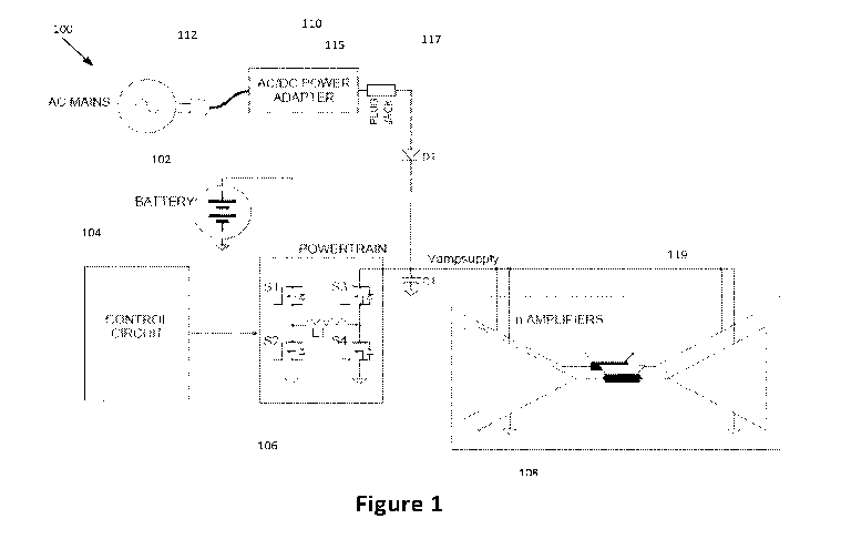
[0030] Figure 1 schematically illustrates a battery powered audio
amplifier system
100 (hereinafter "system 100") in accordance with various embodiments. The
system
CA 03072068 2020-02-04
WO 2019/032380 PCT/US2018/045060
may include a rechargeable battery 102, a control circuit 104, a switching
power
conversion circuit 106 (also referred to as powertrain 106), one or more
amplifiers 108,
and an AC/DC adapter 110, coupled to one another as shown. For example, the
power
conversion circuit 106 may be coupled between the battery 102 and the one or
more
amplifiers 108 and between the battery 102 and the AC/DC adapter 110. The
control
circuit 104 may be coupled to the power conversion circuit 106. The AC/DC
adapter
110 may be coupled with the power conversion circuit 106 and the one or more
amplifiers 108 (e.g., via a diode D1).
[0031] In various embodiments, the AC/DC adapter 110 may be selectively
coupled to an external power supply 112 (e.g., AC mains, such as a wall
socket), and
may convert the AC voltage from the external power supply to a DC input supply
voltage. The DC input supply voltage may have any suitable value, such as,
without
limitation, 15 Volts (V) in one example. During the charge mode, the AC/DC
adapter
110 may provide the DC input supply voltage to the power conversion circuit
106 and to
the one or more amplifiers 108 (e.g., as the amplifier supply voltage). The
one or more
amplifiers 108 may operate (e.g., drive one or more speaker drivers coupled to
the
respective amplifiers 108) using the DC input supply voltage. Additionally,
the power
conversion circuit 106 may use the DC input supply voltage to charge the
battery 102
(e.g., in cooperation with the control circuit 104).
[0032] In some embodiments, the AC/DC adapter 110 may be removably
coupled to the one or more amplifiers 108 and power conversion circuit 106,
for
example via a plug 115 and jack 117. Such an AC/DC adapter may be referred to
as a
"brick" AC/DC adapter, and may be external to a housing that encompasses the
battery
102, control circuit 104, power conversion circuit 106, and one or more
amplifiers 108.
In other embodiments, the AC/DC adapter 110 may be permanently coupled to the
one
or more amplifiers 108 and the power conversion circuit 106. In some such
embodiments, the AC/DC adapter 110 may be enclosed within the housing of the
battery-powered audio device.
[0033] In some embodiments, the control circuit 104 may control the power
conversion circuit 106 to reduce or increase the amount (e.g., rate) of
current consumed
from the AC/DC adapter for charging the battery 102. For example, the amount
of
6
CA 03072068 2020-02-04
WO 2019/032380 PCT/US2018/045060
current consumed from the AC/DC adapter 110 by the sum total of the power
conversion circuit 106 and the amplifiers 108 may be monitored, and the
control circuit
104 may adjust (e.g., using a feedback or feed-forward loop) the switch timing
of the
power conversion circuit 106 to maintain regulation of this AC/DC adapter
current in
order to maximize the rate of battery charging while not exceeding the current
rating of
the AC/DC power adapter (in some cases, with a safety margin). In some
embodiments, the control circuit 104 may adjust the amount of current drawn by
the
power conversion circuit 106 to charge the battery 102 based on the amount of
current
that is drawn by the one or more amplifiers 108. The current drawn by the one
or more
amplifiers 108 may be determined directly or estimated based on one or more
operating
conditions of the system 100, such as one or more parameters of the audio
signal (e.g.,
a moving average of the rms (e.g., for Class D amplifiers) or average (e.g.,
for Class A,
AB, or B amplifiers) voltage of the input audio signals provided to the
amplifiers 108 or
the output audio signal generated by the amplifiers 108), and/or one or more
other
suitable operating parameters.
[0034] During the discharge mode of the system 100, the AC/DC adapter 110
may not be coupled to the external power supply and/or to the power conversion
circuit
106 and one or more amplifiers 108 (e.g., when the AC/DC adapter is an
external
"brick" adapter that is disconnected from the housing of the audio device).
Accordingly,
the power conversion circuit may generate an amplifier supply voltage
(Vampsupply)
from the voltage provided by the battery 102 and provide the amplifier supply
voltage to
the one or more amplifiers 108. The one or more amplifiers 108 may operate
using the
amplifier supply voltage. The battery 102 may provide any suitable battery
voltage,
such as, without limitation, 7.2V in one example.
[0035] In various embodiments, the amplifier supply voltage provided by
the
power conversion circuit 106 may be regulated based on one or more operating
conditions, such as the system volume setting and/or one or more parameters of
the
audio signal (e.g., the magnitude of the audio signal at the input or output
of the
amplifiers 108, a time-advance envelope of the upcoming audio signal, and/or
one or
more other suitable parameters). For example, the power conversion circuit 106
may
provide the regulated amplifier supply voltage with a voltage level that is
less than the
7
CA 03072068 2020-02-04
WO 2019/032380 PCT/US2018/045060
battery supply voltage when permitted based on the one or more operating
conditions
(e.g., for a relatively low volume level or audio signal level), thereby
consuming less
power than if the amplifier supply voltage were kept at a constant value
(e.g., at the
battery supply voltage). In some embodiments, the regulated amplifier supply
voltage
may not be lowered to less than a minimum voltage, which may correspond to a
minimum voltage required for proper function of the amplifiers 108 (e.g., even
at low
volume level or audio signal level).
[0036] Additionally, or alternatively, in some embodiments, the power
conversion
circuit 106 may provide the regulated amplifier supply voltage with a voltage
value that
is greater than the battery supply voltage when dictated by the one or more
operating
conditions (e.g., at a relatively high volume level or audio signal level),
thereby enabling
the amplifiers 108 to achieve higher peak output power than if the amplifier
supply
voltage were limited to the battery supply voltage. Accordingly, in some
embodiments,
the power conversion circuit 106 may be capable of providing the regulated
amplifier
supply voltage with a voltage level that is less than, equal to, or greater
than the battery
supply voltage depending on the one or more operating conditions.
[0037] As shown in Figure 1, one implementation of the power conversion
circuit
106 may include transistors (e.g., metal-oxide-semiconductor field-effect
transistors
(MOSFETs) S1-S4, and an inductor L1. Although the power conversion circuit 106
is
described herein with reference to MOSFETs, other embodiments may include
another
suitable type of transistors. In some embodiments, the battery 102 may be
coupled to a
drain terminal of the MOSFET Si, and the power rail of the amplifiers 108 may
be
coupled to a drain terminal of the MOSFET S3 to receive the amplifier supply
voltage
Vampsupply during the discharge mode. The drain terminal of the MOSFET S2 may
be
coupled with the source terminal of the MOSFET Si, and the drain terminal of
the
MOSFET S4 may be coupled with the source terminal of the MOSFET S3. The
inductor
L1 may be coupled between a first node that is between the MOSFETS Si and S2
and
a second node that is between the MOSFETS S3 and S4. The control circuit 104
may
provide respective drive signals to the gate terminals of the MOSFETS S1-S4 to
control
operation of the power conversion circuit 106. The operation of the power
conversion
circuit 106 will be further described below with respect to Figure 2.
8
CA 03072068 2020-02-04
WO 2019/032380 PCT/US2018/045060
[0038] In some embodiments, MOSFET S2 in the power conversion circuit 106
may be replaced with a diode.
[0039] In various embodiments, the system 100 may provide a single
control
circuit 104 and a single power conversion circuit 106, in contrast with prior
systems that
employed separate control circuits and power conversion circuits for charging
and for
driving the amplifiers, respectively. Accordingly, the system 100 may include
one fewer
control circuit and one fewer inductor than prior designs, thereby reducing
the cost, size,
and implementation complexity of the system 100 compared with prior systems.
In
some embodiments, the control circuit 104 and the power conversion circuit 106
less
the inductor may be disposed on a single integrated circuit (IC). In other
embodiments,
the control circuit 104 and the power conversion circuit 106 less the inductor
may be
disposed on two different ICs. In other embodiments, aspects of the control
circuit 104
may be disposed on different ICs that are coupled with one another.
[0040] Furthermore, the variable regulated amplifier supply voltage
provided by
the power control circuit 104 and power conversion circuit 106 may reduce
power
consumption of the system 100, thereby prolonging the battery run time of the
battery
102 and/or allowing for a smaller capacity battery 102 to be used in the
system 100.
Additionally, the peak current demands from the AC/DC adapter 110 may be
reduced
compared with prior systems, thereby permitting a reduction in the size and
cost of the
AC/DC adapter. Moreover, the regulated amplifier supply voltage may enable
higher
peak output power for the one or more amplifiers 108 when needed, while also
providing power savings when possible.
[0041] In various embodiments, the one or more amplifiers 108 may have
any
suitable amplifier topology, such as a linear type amplifier (e.g., Class A,
Class AB,
Class 6), a switching type amplifier (e.g. Class D), another suitable type of
amplifier,
and/or a combination of amplifier types. In embodiments that include multiple
amplifiers
108, the amplifiers 108 may be bridged, as shown in Figure 1. The amplifiers
108 may
operate from the same, unipolar supply bus to receive the amplifier supply
voltage. The
amplifiers 108 may be coupled to respective speaker drivers 119 to drive the
speaker
drivers 119 based on the input audio signals received by the respective
amplifiers 108.
9
CA 03072068 2020-02-04
WO 2019/032380 PCT/US2018/045060
[0042] Figure 2 illustrates a portable battery-powered audio system 200
(hereinafter "system 200") in accordance with various embodiments. System 200
may
be an example implementation of the system 100 described above with reference
to
Figure 1. For example, the system 200 may include a battery 202 that
corresponds to
the battery 102, a power conversion circuit (powertrain) 206 that corresponds
to the
power conversion circuit 106, amplifiers 208 that correspond to the amplifiers
108, and
AC/DC converter 210 that corresponds to the AC/DC converter 110. Some or all
remaining circuit blocks shown in Figure 2 may be included in a control
circuit that may
correspond to the control circuit 104 of system 100.
[0043] In various embodiments, the AC/DC converter may be selectively
coupled
to an AC supply voltage 212 (e.g., a wall socket). As previously discussed
with respect
to system 100, the system 200 may be switchable between a discharge mode, in
which
the amplifier supply voltage Vampsupply is provided by the power conversion
circuit 206
from the battery 202, and a charge mode, in which the amplifier supply voltage
Vampsupply is provided by the AC/DC power adapter 210 and the power conversion
circuit 206 charges the battery 202. The system 200 may determine whether the
system 200 is in the discharge mode or the charge mode based on voltage
Vadapter.
The voltage Vadapter may be provided by the AC/DC adapter, and may correspond
to
the amplifier supply voltage Vampsupply provided by the AC/DC adapter 210
while the
AC/DC adapter is coupled to the AC supply voltage 212 and the amplifiers 208,
thereby
indicating that the external power source (the AC supply voltage 212) is
connected to
the system 200.
[0044] In various embodiments, the system 200 shown in Figure 2 may
adjust the
amplifier supply voltage (Vampsupply) provided to the amplifiers 208 during
the
discharge mode based on the volume level setting of the system 200 (e.g., as
set by the
user). For example, in some embodiments, the system 200 may regulate the
amplifier
supply voltage to be proportional to the volume level setting plus an offset,
and subject
to a minimum value.
[0045] As shown in Figure 2, a system volume register 214 may store the
volume
level setting. The volume level setting may be set by a user of the system 200
using a
volume interface 216. The volume interface 216 may include, for example, one
or more
CA 03072068 2020-02-04
WO 2019/032380 PCT/US2018/045060
buttons, a wireless interface (e.g., to interact with an electronic device
such as a
smartphone, an application on an electronic device, and/or a dedicated remote
control),
a touchscreen, a microphone (e.g., to receive voice commands from the user),
and/or
another suitable interface. In some embodiments, the system volume register
214 may
be included in the battery-powered audio device that implements the system
200. In
other embodiments, the system volume register 214 may be included in an
external
device (e.g., smartphone), and the system 200 may receive the volume level
setting that
is stored in the system volume register 214 from the external device.
[0046] An offset value (e.g., stored in an offset register 218) may be
added to the
volume level setting at block 220, and the resulting value may be stored in a
register
222. Block 224 determines the larger value between the value stored in the
register
222 (corresponding to the volume level plus the offset value) and a minimum
supply
voltage value (e.g., stored in a register 226), and passes the larger value to
a target
supply register 228. A digital-to-analog (DAC) converter 230 may convert the
target
value stored in the target supply register 228 to an analog target supply
voltage
(Vsupplytarget). The registers 214, 218, 222, 226, and 228 may be continually
updated
(e.g., responsive to a clock signal and/or responsive to a change in the
volume level
setting stored by the system volume register 214) to provide an updated value
for the
target supply voltage.
[0047] In the embodiment shown in Figure 2, the registers 214, 218, 222,
226,
and 228 may be digital registers, and the corresponding values stored in the
respective
registers may be digital values. However, it will be apparent that in other
embodiments,
one or more of the registers may be an analog register. Additionally, or
alternatively,
aspects of the system 200, such as one of more of the registers, may be
implemented
in software and/or firmware.
[0048] In various embodiments, the target supply voltage Vsupplytarget
corresponds to the intended supply voltage to be applied to the amplifiers by
the system
200 during the discharge mode, as further discussed below. For example, the
amplifier
supply voltage Vampsupply that is provided to the amplifiers 208 during the
discharge
mode may be substantially proportional to the target supply voltage
Vsupplytarget.
11
CA 03072068 2020-02-04
WO 2019/032380 PCT/US2018/045060
[0049] In various embodiments, the target supply voltage Vsupplytarget
may be
provided to a first input terminal of discharge error amplifier 232. A second
input
terminal of the discharge error amplifier 232 may receive a version of the
amplifier
supply voltage Vampsupply (e.g., a scaled-down version of the amplifier supply
voltage
Vampsupply as provided by resistors R5 and R6). The discharge error amplifier
232
may generate an error voltage VerrD that indicates (e.g., is proportional to)
a difference
between the version of the amplifier supply voltage Vampsupply and the target
supply
voltage Vsupplytarget. Accordingly, the error voltage VerrD may indicate how
the
amplifier supply voltage needs to be adjusted to arrive at its target value.
[0050] In various embodiments, the discharge error amplifier 232 may
provide the
error voltage VerrD to a discharge current-mode pulse-width modulation (PWM)
modulator 234. The discharge current-mode PWM modulator 234 may further
receive a
voltage signal Vr1 that indicates a peak current through the inductor L1 of
the power
conversion circuit 206. The discharge current-mode PWM modulator 234 may
generate
a discharge-mode variable pulse-width modulated (PWM) signal VpwmD based on
the
error voltage VerrD and the peak current through the inductor L1 as indicated
by the
voltage signal Vr1. The signal VpwmD may be used to control the power
conversion
circuit 206 (e.g., to control the switching time of the MOSFETs S1-S4 and the
peak
current in inductor L1) to generate the amplifier supply voltage Vampsupply
with the
target voltage level during the discharge mode.
[0051] In various embodiments, a resistor R1 may be coupled between the
source terminal of MOSFET S4 and ground to provide the voltage signal Vr1
(e.g., from
the node between the resistor R1 and the MOSFET S4) to implement a peak-
current-
mode control PWM scheme during discharge mode. During the discharge mode,
resistor R2, which may be coupled between the source terminal of MOSFET S2 and
ground, may be used to sense the current going to the amplifiers 108 (e.g.,
via the
amplifier supply voltage Vampsupply) in order to control a synchronous-
rectifier scheme
for MOSFETs S2 and S3.
[0052] In various embodiments, the discharge-mode variable PWM signal
VpwmD may be passed to an input terminal of a multiplexer 236. The multiplexer
236
may also receive a charge-mode variable PWM signal VpwmC (further discussed
12
CA 03072068 2020-02-04
WO 2019/032380 PCT/US2018/045060
below) at another input terminal and may further receive the signal Vadapter
at a
selection terminal. When the signal Vadapter indicates that the system 200 is
in the
discharge mode (e.g., when the AC/DC adapter is not providing power and
Vadapter is
consequently logic low), the multiplexer may pass the discharge-mode variable
PWM
signal to its output terminal (e.g., as Vpwm) to control the power conversion
circuit 206
(e.g., via drive logic 238 and/or a MOSFETs driver 240).
[0053] In contrast, if the signal Vadapter indicates that the system 200
is in the
charge mode (e.g., when Vadapter is logic high), then the multiplexer 236 will
pass the
charge-mode variable PWM signal VpwmC to its output terminal (e.g., as Vpwm).
In
various embodiments, charge-mode circuitry of the system 200 may include a
constant
current (CC) charge error amplifier 242, a constant voltage (CV) charge error
amplifier
244, and a charge current-mode PWM modulator 246. The battery voltage Vbattery
may be sensed by resistors R12 and R13 and passed to an input terminal of the
CV
charge error amplifier 244. The CV charge error amplifier 244 may receive a CV
reference voltage Vref_cv at another input terminal and generate a CV error
signal
based on the comparison. The CV error signal from the CV charge error
amplifier 244
may be provided to the charge current-mode PWM modulator 246 to regulate the
battery voltage Vbattery to be no more than a target voltage that is
proportional to
Vref_cv.
[0054] The CC charge error amplifier 242 may compare the output current
magnitude of the AC/DC adapter 210 (e.g., provided as a voltage by resistor R3
using
ground-side sensing) with a target current magnitude (e.g., that is
proportional to
reference voltage Vref_cc). The target current may correspond to a rated
output current
of the AC/DC adapter 210 (with or without a safety margin subtracted) and the
CC
charge error amplifier 242 may output an error signal based on the comparison.
The
reference voltage Vref_cc may correspond to a voltage resulting from passing
the target
current through the resistor R3. The error signal from the CC charge error
amplifier 242
may be provided to the charge current-mode PWM modulator 246 to regulate the
output
current of the AC/DC adapter 210 to no more than the target current. In some
embodiments, the one of the error signal from the CC charge error amplifier
242 or the
error signal from the CV charge error amplifier 244 having the lesser value
may be
13
CA 03072068 2020-02-04
WO 2019/032380 PCT/US2018/045060
provided to the charge current-mode PWM modulator 246 as a charge error signal
VerrC. For example, the output terminals of the CC charge error amplifier 242
and the
CV charge error amplifier 244 may be coupled to the VerrC input terminal of
the charge
current-mode PWM modulator 246 via respective diodes D2 and D3. In the charge
mode, the circuitry of system 200 may enable the AC/DC adapter 210 to supply
power
to the amplifiers (e.g., the amplifier supply voltage Vampsupply provided via
diode D1)
while also charging the battery as quickly as possible without exceeding the
AC/DC
adapter current rating.
[0055] For example, when the battery voltage is low, the CV charge error
amplifier 244 may saturate to a high output voltage. The CC charge error
amplifier 242
may provide its error signal to the charge current-mode PWM modulator 246,
permitting
the battery 202 to charge as fast as the current limit of the AC/DC adapter
210 will
permit. As the battery voltage rises to its maximum, the CV charge error
amplifier 244
will begin to provide its error signal to the charge current-mode PWM
modulator 246
instead of the error signal from the CC charge error amplifier 242, to
gradually reduce
the PWM index provided by the charge current-mode PWM modulator 246 to taper
down the charging current while maintaining the battery voltage at the target
maximum.
[0056] In various embodiments, the charge current-mode PWM modulator may
generate the charge-mode PWM signal VpwmC based on the charge error signal
VerrC
and a signal Vr2 that indicates the peak current through inductor L1 of the
power
conversion circuit 206. The signal Vr2 may be provided by resistor R2.
Resistor R1 of
the power conversion circuit 206 may be used to sense the current going from
the
power conversion circuit 206 to the battery 202 in order to control a
synchronous-
rectifier scheme for MOSFETs Si and S4.
[0057] In some embodiments, one or more additional or alternative limits
on the
battery-charging current may be imposed in the charge current-mode PWM
modulator
246. For example, in some cases, the maximum battery charge current may be
limited
to less than the current rating of the AC/DC adapter 210 in order to not
exceed the
charge-current rating of the battery 202.
[0058] Additionally, or alternatively, in some embodiments, during the
discharge
mode and when the target supply voltage is lower than the battery voltage
Vbattery, the
14
CA 03072068 2020-02-04
WO 2019/032380 PCT/US2018/045060
MOSFET S3 of the power conversion circuit 206 may remain ON (e.g., for a
complete
clock cycle) and the MOSFET S4 may remain OFF. The MOSFET Si ON time pulse
width may be modulated (e.g., by the discharge current-mode PWM modulator) and
the
MOSFET S2 may be used as a synchronous rectifier. Accordingly, the power
conversion circuit 206 may behave as a buck converter.
[0059] Additionally, or alternatively, in some embodiments, during the
discharge
mode and when the target supply voltage is higher than the battery voltage
Vbattery,
the MOSFET Si may remain ON and the MOSFET S2 may remain OFF. The MOSFET
S4 ON time pulse width may be modulated (e.g., by the discharge current-mode
PWM
modulator) and the MOSFET S3 may be used as a synchronous rectifier.
Accordingly,
the power conversion circuit 206 may behave as a boost converter.
[0060] In other embodiments, the MOSFETs S1-S4 of the power conversion
circuit 206 may be activated (e.g., by the drive logic 238) in another
suitable fashion
familiar to those skilled in the art of power conversion in order to achieve a
regulated
amplifier supply voltage Vampsupply that is higher, lower, or equal to the
battery voltage
Vbattery.
[0061] In various embodiments, the amplifiers 208 are powered using the
amplifier supply voltage Vampsupply to generate respective amplifier output
signals Va,
Vb, Vc, and Vd, based on respective amplifier input signals (e.g., received
from an
audio processor). The amplifier output signals are passed to respective
speaker drivers
248 to drive the speaker drivers.
[0062] Figure 3 illustrates a discharge current-mode PWM modulator circuit
300
that may be used in some embodiments of the discharge current-mode PWM
modulator
234. As discussed above with respect to the discharge current-mode PWM
modulator
234, the discharge current-mode PWM modulator circuit 300 may generate a
discharge-
mode variable PWM signal VpwmD based on the error voltage VerrD and the peak
current through the inductor Li as indicated by the voltage signal Vr1. Other
modulation schemes may be used in other embodiments, such as a voltage-mode
PWM
scheme, variable-frequency constant-on-time pulse-density modulation, and/or
another
modulation scheme known to those skilled in the art of power conversion.
CA 03072068 2020-02-04
WO 2019/032380 PCT/US2018/045060
[0063] Figure 4 illustrates a charge current-mode PWM modulator circuit
400 that
may be used in some embodiments of the charge current-mode PWM modulator 246.
As discussed above with respect to the charge current-mode PWM modulator 246,
the
charge current-mode PWM modulator circuit 400 may generate the charge-mode PWM
signal VpwmC based on the charge error signal VerrC and the peak current
through
inductor L1 of the power conversion circuit as indicated by the signal Vr2.
Similar to the
discharge current-mode PWM modulator circuit 300, other modulation schemes may
be
used in other embodiments, such as a voltage-mode PWM scheme, variable-
frequency
constant-on-time pulse-density modulation, and/or another modulation scheme
known
to those skilled in the art of power conversion.
[0064] Figure 5 illustrates a drive logic circuit 500 that may be used for
the drive
logic 238 of system 200 in some embodiments. The drive logic circuit 500 may
provide
drive signals for the MOSFETS S1-54 of the power conversion circuit (e.g.,
power
conversion circuit 206) based on the PWM signal Vpwm and the Vadapter signal
that
indicates whether the system is in the charge mode or the discharge mode. The
drive
logic circuit 500 may provide a first drive signal (V_S1,S4) to the MOSFETs Si
and S4
of the power conversion circuit 206, e.g., to turn the MOSFETs Si and S4 ON or
OFF
simultaneously. Additionally, the drive logic circuit 500 may provide a second
drive
signal (V_S2,53) to the MOSFETs S2 and S3, e.g., to turn the MOSFETs S2 and S3
ON or OFF simultaneously. The Vadapter signal determines which pair of MOSFETs
is
turned ON according to the Vpwm signal. Synchronous rectification signals may
be
generated by the drive logic circuit 500 to turn ON the opposing pair of
MOSFETs when
the Vpwm signal goes low, then turn them OFF when either the inductor current
falls to
zero or the Vpwm signal goes high again.
[0065] Figure 6 illustrates example waveforms 600 for various signals of
the
system 200 of Figure 2 during the discharge mode, in accordance with various
embodiments. The waveforms 600 include the first drive signal V_S1,S4, the
second
drive signal 52,S3, the current (I_L1) through the inductor L1 of the power
conversion
circuit 206, and the amplifier supply voltage Vampsupply. For the example
waveforms
600 shown in Figure 6, synchronous rectification is used in the drive logic
block 238.
The MOSFETs Si and S4 turn ON for a period of time and the current in the
inductor L1
16
CA 03072068 2020-02-04
WO 2019/032380 PCT/US2018/045060
increases. The MOSFETs Si and S4 then turn OFF after the period of time, and
the
MOSFETs S2 and S3 turn ON in order to permit the inductor current in inductor
L1 to
flow to the Vampsupply node (e.g., in accordance with synchronous
rectification
principles) with very little voltage drop. The MOSFETs S2 and S3 then turn off
when
the inductor current falls to zero. The average Vampsupply voltage in this
embodiment
is regulated proportional to Vsupplytarget set by the system volume position
and the
offset, and is adequately high enough to supply voltage to the amplifier and
avoid
clipping collisions between the amplifier output signals Va, Vb, Vc, and Vd
and the
Vampsupply voltage.
[0066] Figure 7 illustrates example waveforms 700 for various signals of
the
system 200 of Figure 2 during the charge mode. The waveforms 700 include the
first
drive signal V_S1,S4, the second drive signal S2,53, the current (I_L1)
through the
inductor L1 of the power conversion circuit 206, and the amplifier supply
voltage
Vampsupply. For the example waveforms 700 shown in Figure 7, synchronous
rectification is used in the drive logic block 238. The MOSFETs S2 and S3 turn
on for a
period of time and the current in the inductor L1 goes negative with
increasing
magnitude. The MOSFETs S2 and S3 then turn OFF after the period of time, and
the
MOSFETs Si and S4 turn ON in order to permit the current in the inductor L1 to
flow to
Vbattery (e.g., in accordance with synchronous rectification principles) with
very little
voltage drop, and thereby charge the battery. The MOSFETs Si and S4 then turn
off
when the magnitude of the current in the inductor L1 falls to zero. The
Vampsupply
voltage in this embodiment is equal to the output voltage of the AC/DC adapter
less a
diode drop due to diode Dl. The Vampsupply voltage is high enough to supply
voltage
to the amplifier and avoid clipping collisions between the amplifier output
signals Va, Vb,
Vc, and Vd and the Vampsupply voltage.
[0067] Figure 8 illustrates example waveforms 800 for various signals in
the
system 200 when the volume setting is adjusted (e.g., by the user), in
accordance with
some embodiments. The example waveforms 800 include the volume setting stored
in
the system volume register, the target supply voltage Vsupplytarget, the
amplifier supply
voltage Vampsupply, and the amplifier output voltage signal Va. In this
embodiment,
the volume setting stored in the system volume register is represented by a 3-
bit digital
17
CA 03072068 2020-02-04
WO 2019/032380 PCT/US2018/045060
value. It will be apparent that a different number of bits may be used for the
volume
setting in other embodiments. Additionally, or alternatively, in some
embodiments, the
volume setting stored in the system volume register may be down-sampled from
the
actual volume setting on the audio device. For example, the audio device may
have
more available volume settings (e.g., corresponding to more bits) than the
available
volume settings (e.g., corresponding to the number of bits) that may be stored
in the
system volume register.
[0068] Figure 9 illustrates another example of a portable battery-powered
audio
system 900 (hereinafter "system 900") in accordance with various embodiments.
System 900 may be another example implementation of the system 100 described
above with reference to Figure 1. The system 900 may set the voltage level of
the
amplifier supply voltage Vampsupply during the discharge mode based on the
audio
signal that is processed by the amplifiers 908.
[0069] For example, the system 900 may generate a supply target voltage
that
corresponds to a peak value of the amplifier output voltage. In some
embodiments, a
peak-hold-with-decay scheme may be used to generate the supply target voltage
based
on the amplifier output voltage, e.g., so that the supply target voltage
lowers more
slowly after a peak in the amplifier output voltage. In some embodiments, the
supply
target voltage may correspond to the peak value of the amplifier output
voltage plus an
offset voltage. Additionally, or alternatively, the supply target voltage may
be subject to
a minimum voltage. That is, the system 900 may set the supply target voltage
as the
greater of the minimum voltage or the value that corresponds to the peak value
of the
amplifier output voltage (e.g., plus an offset voltage). In embodiments of the
system
900 in which multiple amplifier channels share the amplifier supply voltage
Vampsupply,
the system 900 may determine the supply target voltage based on the amplifier
output
voltage having the peak of the greatest magnitude (e.g., at any given time
using the
peak-hold-with-decay scheme).
[0070] As an example implementation of this control scheme, the system 900
may include target supply circuitry 950 to generate the target supply voltage.
The target
supply circuitry 950 may receive the amplifier output voltages Va, Vb, Vc, and
Vd from
the respective amplifiers 908. An addition block 952 may receive the amplifier
output
18
CA 03072068 2020-02-04
WO 2019/032380 PCT/US2018/045060
voltages via respective diodes D4, D5, D6, and D7, thereby effectively passing
the
maximum value from among the amplifier output voltages to the addition block
952.
After a peak in the maximum amplifier output voltage, the voltage level
received by the
addition block 952 may decay according to a time constant provided by
capacitor C20
and resistor R20.
[0071] The addition block 952 may add an offset voltage Voffset to the
maximum
amplifier output voltage and the generated voltage may be coupled to a target
voltage
node 954 via a diode D8. A minimum voltage Vmin may also be coupled to the
target
voltage node 954 via another diode D9. Accordingly, the target voltage node
954 may
receive the greater of the minimum voltage Vmin or the output voltage from the
addition
block 952 (which corresponds to the maximum amplifier output voltage plus the
offset
voltage Voffset). The resulting target supply voltage Vsupplytarget at the
target voltage
node 954 may be passed to the discharge error amplifier 932, which may be
similar to
the discharge error amplifier 232 of system 200. The discharge error amplifier
932 may
generate an error signal VerrD based on the target supply voltage
Vsupplytarget and
the amplifier supply voltage Vampsupply, in order to provide the amplifier
supply voltage
with a regulated voltage level that is substantially proportional to the
target supply
voltage Vsupplytarget.
[0072] Accordingly, when in discharge mode, the target supply voltage
Vsupplytarget generated by the target supply circuitry 950 may cause the
amplifier
supply voltage Vampsupply to follow an envelope of the largest-magnitude of
the
amplifier output voltages, wherein Vampsupply rises rapidly as needed during a
large
amplifier output voltage transient, then decays gradually (e.g., according to
the time
constant provided by capacitor C20 and resistor R20) until another large
transient
occurs.
[0073] The remaining components of the system 900 may be similar to
corresponding components of the system 200 discussed above, and thus will not
be
described again here.
[0074] In another embodiment, the target supply voltage may be determined
based on a forward-looking version of the audio signal. For example, the peak-
hold-
with-decay function and the comparison with the minimum voltage may be
performed in
19
CA 03072068 2020-02-04
WO 2019/032380 PCT/US2018/045060
the digital domain, e.g., using digital delay memory to effectively create
time-advanced
audio signals to permit the power conversion circuitry to slew the amplifier
supply
voltage Vampsupply at capacitor Cl to a higher target value prior to the
amplifier
reproducing the corresponding audio signal levels (e.g., on the order of a few
milliseconds or tenths of milliseconds prior).
[0075] In some embodiments, the target supply voltage Vtargetsupply may
be
digitized such that the amplifier supply voltage Vampsupply is regulated to
one of a
number of discrete voltage levels (e.g., proportional to the envelope of the
audio signals
being reproduced). Additionally, or alternatively, while the system 900 is
described with
reference to determining the target supply voltage Vtargetsupply based on the
amplifier
output voltages, other embodiments may determine the target supply voltage
Vtargetsupply based on one or more other or additional operating parameters,
such as
the amplifier analog input voltages (associated with the audio signals), a
combination of
the amplifier input and output voltages, and/or the difference between the
amplifier
output voltage and the amplifier supply voltage Vampsupply.
[0076] Figure 10 illustrates an example of a battery-powered audio system
1000
(hereinafter "system 1000") that, in discharge mode, may selectively operate
the power
conversion circuit 1006 as a buck converter (e.g., when the target supply
voltage is
lower than the battery voltage Vbattery) or a boost converter (e.g., when the
target
supply voltage is higher than the battery voltage Vbaitery), or, in charge
mode, as a
buck converter transferring power from the AC/DC Power Adapter to the battery,
as
described above.
[0077] For example, the System 1000 may be another example implementation
of the system 100 described above with reference to Figure 1. The system 1000
may
be similar to the system 100 and/or 900 depicted in Figures 1 and 9,
respectively,
except that the system 1000 includes a mode selection circuit 1051 to
determine
whether the target supply voltage is greater or less than the battery voltage
and to
control the power conversion circuit 1006 (e.g., via the drive logic 1038) to
operate in
the buck mode or the boost mode based on the determination.
[0078] For example, the mode selection circuit 1051 may include a
comparator,
as shown in Figure 10, to compare the target supply voltage to the battery
voltage (e.g.,
CA 03072068 2020-02-04
WO 2019/032380 PCT/US2018/045060
a voltage divided version of the battery voltage provided by resistors R50 and
R51).
The output of the comparator may be passed to the drive logic 1038. If the
target
supply voltage is lower than the battery voltage Vbattery, the mode selection
circuit
1051 may control the MOSFET S3 of the power conversion circuit 1006 to remain
ON
(e.g., for a complete clock cycle) and the MOSFET S4 to remain OFF. The MOSFET
Si ON time pulse width may be modulated (e.g., by the discharge current-mode
PWM
modulator) and the MOSFET S2 may be used as a synchronous rectifier.
Accordingly,
the power conversion circuit 1006 may behave as a buck converter.
[0079] However, if the target supply voltage is higher than the battery
voltage
Vbattery, the mode selection circuit 1051 may control the MOSFET Si to remain
ON
and the MOSFET S2 to remain OFF. The MOSFET S4 ON time pulse width may be
modulated (e.g., by the discharge current-mode PWM modulator) and the MOSFET
S3
may be used as a synchronous rectifier. Accordingly, the power conversion
circuit 1006
may behave as a boost converter.
[0080] Additionally, or alternatively, in some embodiments, during the
charge
mode, the control circuitry may control the power conversion circuit 1006 to
operate as
a buck converter (e.g., in the reverse direction from the discharge mode,
referred to as
a charge buck mode). That is, transistor S3 may be modulated as PWM buck
converter,
S4 modulated as synchronous rectifier, Si ON (e.g. for a complete clock
cycle), and S2
OFF (e.g. for a complete clock cycle). The buck converter functionality of the
power
conversion circuit 1006 is not specific to the embodiment of Figure 10, and
may also be
used by the power conversion circuits described elsewhere herein in some
embodiments (e.g., in the embodiments of Figures 1, 2, and/or 9).
[0081] Figure 11 shows switching control circuitry 1100 that may be used
to
control the transistors (e.g., Si, S2, S3, and S4) of a power conversion
circuit (e.g.
power conversion circuit 1006 or another power conversion circuit described
herein) to
selectively operate in a boost mode or buck mode as described above with
respect to
Figure 10. For example, the switching control circuitry 1100 may be included
in drive
logic 1038 in some embodiments. As shown, the switching control circuitry 1100
may
include a pair of multiplexers 1102 and 1104 to provide the switching control
signals to
the respective gate terminals of the switching transistors. The switching
control circuitry
21
CA 03072068 2020-02-04
WO 2019/032380 PCT/US2018/045060
1100 may include discharge synchronous recitifier control circuitry 1106 and
1108 to
selectively operate respective transistor S2 or transistor S3 as synchronous
rectifiers
during the discharge mode, as described herein. The switching control
circuitry 1100
may further include a charge synchronous rectifier control circuitry 1110 to
selectively
operate the transistor S4 as a synchronous rectifier during the charge mode,
as
described herein.
[0082] Figure 12 illustrates example waveforms 1200 for various signals of
the
system 1000 to operate the power conversion circuit 1006 in the buck mode
during the
discharge mode (e.g., when the target supply voltage is less than the battery
voltage), in
accordance with various embodiments. The waveforms 1200 may be an alternative
to
waveforms 600 of Figure 6. The waveforms 1200 include the drive signals V_S1,
V_S2,
V_S3, and V_S4 to control respective transistors Si, S2, S3, and S4 of the
power
conversion circuit 1006, the current (I_L1) through the inductor L1 of the
power
conversion circuit 1006, and the amplifier supply voltage Vampsupply.
[0083] Figure 13 illustrates example waveforms 1300 for various signals of
the
system 1000 to operate the power conversion circuit 1006 in the boost mode
during the
discharge mode (e.g., when the target supply voltage is greater than the
battery
voltage), in accordance with various embodiments. The waveforms 1300 may be an
alternative to waveforms 600 of Figure 6. The waveforms 1300 include the drive
signals
V_S1, V_S2, V_S3, and V_S4 to control respective transistors Si, S2, S3, and
S4 of
the power conversion circuit 1006, the current (I_L1) through the inductor L1
of the
power conversion circuit 1006, and the amplifier supply voltage Vampsupply.
[0084] Figure 14 illustrates example waveforms 1400 for various signals of
the
system 1000 to operate the power conversion circuit 1006 in the buck mode
during the
charge mode, in accordance with various embodiments. The waveforms 1400 may be
an alternative to waveforms 700 of Figure 7. The waveforms 1400 include the
drive
signals V_S1, V_S2, V_53, and V_S4 to control respective transistors Si, S2,
S3, and
S4 of the power conversion circuit 1006, the current (I_L1) through the
inductor L1 of
the power conversion circuit 1006, and the amplifier supply voltage
Vampsupply.
[0085] In various embodiments, the systems described herein may be used
with
any suitable type of audio amplifiers, such as switching types (Class D) or
linear types
22
CA 03072068 2020-02-04
WO 2019/032380 PCT/US2018/045060
(Class A or Class AB or Class B), or a combination thereof. Regardless of the
type of
amplifiers used, the amplifier power dissipation and thereby the system power
dissipation may be reduced by reducing the amplifier supply voltage Vampsupply
used
to supply the amplifier when permissible, as described herein. This reduction
of system
power dissipation increases battery run time for the portable audio device.
[0086] The circuits, systems, and methods disclosed herein may be used in
any
suitable battery-powered audio devices, such as portable battery-powered audio
devices, including, but not limited to wireless audio speakers (e.g., using
any suitable
wireless interface, such as Bluetooth, local area network (LAN, e.g., WiFi),
cellular
(such as Third Generation Partnership Protocol (3GPP) cellular, and/or another
suitable
wireless network interface), smart-home speakers, smartphones, laptop
computers,
and/or other suitable devices. The battery-powered audio device may further
include a
wireless network interface (e.g., using any suitable wireless interface, such
as
Bluetooth, local area network (LAN, e.g., WiFi), cellular (such as Third
Generation
Partnership Protocol (3GPP) cellular, and/or another suitable wireless network
interface) to receive audio signals to be reproduced by the speaker of the
device. An
audio processor circuit may be coupled between the wireless network interface
and the
amplifiers of the device, to process the audio signals received by the
wireless network
interface into a form that is usable by the amplifiers. For example, the audio
processor
may include a digital signal processor to implement audio processing such as
filtering
and delays, and a digital-to-analog converter to convert a digital audio
signal to an
analog audio signal that is processed by the amplifiers. Additionally, or
alternatively, the
battery-powered audio device may include one or more additional components,
such as
one or more processors, memory (e.g., random access memory (RAM), mass storage
(e.g., flash memory, hard-disk drive (HDD), etc.), antennas, etc.
[0087] Although certain embodiments have been illustrated and described
herein,
it will be appreciated by those of ordinary skill in the art that a wide
variety of alternate
and/or equivalent embodiments or implementations calculated to achieve the
same
purposes may be substituted for the embodiments shown and described without
departing from the scope. Those with skill in the art will readily appreciate
that
embodiments may be implemented in a very wide variety of ways. This
application is
23
CA 03072068 2020-02-04
WO 2019/032380
PCT/US2018/045060
intended to cover any adaptations or variations of the embodiments discussed
herein.
Therefore, it is manifestly intended that embodiments be limited only by the
claims and
the equivalents thereof.
24