Note: Descriptions are shown in the official language in which they were submitted.
86015203
1
HIGH-VOLTAGE DEVICE HAVING CERAMIC SPACER
ELEMENTS, AND USE THEREOF
FIELD OF THE INVENTION
The invention relates to a high-voltage device having a housing
and at least one subassembly electrically insulated from the
housing. The at least one subassembly is arranged in a manner
spaced apart from the housing and is mechanically connected to
the housing. The invention furthermore comprises the use of the
high-voltage device described above.
BACKGROUND OF THE INVENTION
High-voltage devices, in particular instrument transformers for
voltages of up to 1200 kV and/or a few thousand amps, are known
e.g. from US 3,525,908. A housing, e.g.. arranged on an insulator,
comprises three-dimensional devices, such as e.g. coils for
measuring high voltages and/or currents. The coils are arranged
around a conductor in the housing, to which conductor high
voltages are applied and/or through which conductor high currents
to be measured flow, the housing being filled with an
electrically insulating medium, e.g. oil, SF6 and/or clean air.
The conductor is in electrical contact with connections on the
insulator and/or on the housing that are electrically insulated
from the housing. The connections are designed for connecting
electrical lines of electrical supply systems, electrical loads
and/or electricity generators. During use, high currents in the
region of a few thousand amps flow via the conductor from one to
the other connection. The high currents in this case can lead to
an intense production of heat on the connections.
CA 3073999 2020-03-30
86015203
2
The housing is electrically insulated from the connections and/or
connectable or connected electrical lines. The connections are
e.g. in the form of an insulated subassembly on the housing, in
particular in the form of a metal plate. The surface of the metal
plate allows cooling with the ambient air and dissipation of the
heat to the surroundings or environment. In order to reduce
heating of the connections, a design made of copper, in
particular with a coating made of nickel, is possible. This
results in high costs and the limited outer surface of the
connections results in limited dissipation of heat to the
surroundings. In the event of high primary currents, heating
above permissible limit values for a temperature can occur and
adequate dissipation of heat via the connections may be
impossible.
SUMMARY OF THE INVENTION
It is an object of the present invention to specify a high-
voltage device and a use thereof that avoid the problems
described above. In particular, it is an object to specify a
high-voltage device whose connections can be - produced
inexpensively, easily, in mechanically robust fashion and
compactly in the form of at least one electrically insulated
subassembly, with high possible dissipation of heat from the
insulated subassembly at the same time.
The indicated object is achieved according to the invention by
a high-voltage device having the features and/or by the use of
the high-voltage device described below.
CA 3073999 2020-03-30
86015203
3
A high-voltage device according to the invention comprises a
housing and at least one subassembly electrically insulated from
the housing. The at least one subassembly is arranged in a manner
.spaced apart from the housing and is connected to the housing in
mechanically robust fashion, in particular. Arranged between the
housing and the at least one subassembly is at least one ceramic
spacer element.
The arrangement of the at least one subassembly in a manner
spaced apart from the housing, with at least one ceramic spacer
element between the housing and the at least one subassembly,
allows good electrical insulation of the at least one subassembly
from the housing, with simultaneously good heat transfer or
thermal conductivity via the at least one ceramic spacer element.
Heat produced on connections of the high-voltage device in the
form of the at least one subassembly e.g. in the event of a large
flow of current can be effectively transferred to the housing
via the at least one ceramic spacer element. The housing serves
as a cold surface, with a large surface area that allows good
dissipation of heat to the environment. The electrically
insulated subassembly can be used to make electrical contact
with elements or components of the high-voltage device, in
particular inside the housing, with the electrically insulated
subassembly forming an inexpensive, simple, mechanically robust
and compact connection or a connecting element.
The ceramic spacer element can be a ceramic disk and/or a ceramic
sleeve and/or a ceramic plate, in particular clamped, in
particular in hollow cylindrical form with a circular base,
=
and/or with a continuous opening along a central axis. The at
least one subassembly can be secured to the housing with the aid
CA 3073999 2020-03-30
86015203
4
of securing means, in particular with the aid of screws and/or
securing means electrically insulated from the subassembly.
Ceramic disks and/or ceramic sleeves and/or ceramic plates that
have an, in particular continuous, in particular circular and/or
rectangular, opening in the center can be used to secure the at
least one subassembly to the housing via screws effectively,
i.e. in mechanically robust and electrically insulated fashion,
the screws each being able to be passed through the continuous,
in particular circular, opening in the ceramic disk and/or
ceramic sleeve. The ceramic disks and/or ceramic sleeves maintain
a fixed, mechanically robust distance between the at least one
subassembly and the housing, and permit electrical insulation of
the at least one subassembly from the housing with simultaneously
good heat exchange between the at least one subassembly and the
housing. This has the associated advantages described above.
The ceramic spacer element can have a high electrical resistance
and a high coefficient of thermal conductivity. This ensures
good electrical insulation of the at least one subassembly from
the housing, with simultaneously good heat exchange between the
at least one subassembly and the housing.
At least one electrical contact-connection element, in
particular at least one screw, can be comprised, for making
electrical contact between the at least one subassembly and at
least one element of the high-voltage device inside the housing.
The high-voltage device can be designed in the style of an
instrument transformer. Electrical elements in the instrument
transformer, i.e. in the housing, e.g. conductors, coils and/or
capacitors, can be in electrical contact with the outer
connection or the at least one subassembly, and in particular
=
CA 3073999 2020-03-30
86015203
electrical lines and/or conductor rails connected thereto, via
the at least one electrical contact-connection element, in
particular via the at least one screw.
The at least one subassembly electrically insulated from the
housing can comprise at least one connecting element for
connecting electrical lines and/or conductor rails, in
particular for electrical connection to electrical supply system
lines, electrical loads and/or electricity generators. This
allows a high-voltage device to be electrically connected in
order to perform a predetermined function according to the type
of device.
The at least one subassembly electrically insulated from the
housing can comprise at least one plate-shaped element, in
particular at least one parallelepipedal plate and/or an L-shaped
element made up of plate-shaped elements. Both connecting
elements and contact-connection elements can be effectively
arranged on, in and/or atop the plate-shaped element, and good
electrical contact between elements can be produced easily and
= inexpensively via the plate-shaped element.
The at least one subassembly electrically insulated from the
housing can be made of a metal, in particular of copper and/or
steel and/or can comprise a metal, in particular copper and/or
steel and/or alloys. This produces good electrical conductivity
and thermal conductivity via the subassembly electrically
insulated from the housing, with the advantages described above.
The housing, in particular a cylindrical housing, can be made of
a metal, in particular cast iron, and/or can comprise a metal,
CA 3073999 2020-03-30
=
86015203
6
in particular cast iron. This produces good thermal conductivity
via the housing, and heat produced on the subassembly
electrically insulated from the housing, e.g. on the electrical
connections and/or connecting surfaces with connecting elements
and/or contact-connection elements and in the subassembly
itself, in the current-carrying state, can be emitted to the
environment effectively via the housing and in particular
effectively via a large surface of the housing.
The at least one ceramic spacer element can be made of an aluminum -
oxide, silicon carbide, boron nitride or aluminum nitride ceramic
and/or can comprise an aluminum oxide, silicon carbide, boron
nitride or aluminum nitride ceramic. These have a high thermal
conductivity, in particular greater than 30 or greater than 100 W
(m x K), and a low electrical conductivity or a high specific
resistance, in particular greater than 1012 ohm-meters or greater
than 1010 ohm-meters at 20 C. This produces good electrical
insulation between the housing and the subassembly electrically
insulated from the housing, with good thermal conductivity or
discharge of excess heat via the ceramic spacer element.
Use, according to the invention, of the high-voltage device
described above involves heat produced on connecting elements of
the at least one subassembly electrically insulated from the
housing, in particular for connecting electrical lines and/or
conductor rails, being transferred from the subassembly to the
housing via the at least one ceramic spacer element and being
emitted from the housing to the environment.
Electrical contact between the at least one subassembly
electrically insulated from the housing and elements in the
CA 3073999 2020-03-30
86015203
V
housing, in particular transformer parts, can be made via at
least one electrical contact-connection element, in particular
via at least one screw, in particular having a current-carrying
capacity in the region of a few thousand amps.
The advantages of the use, in accordance with the invention, of
the high-voltage device are analogous to the advantages described
above of the high-voltage device according to the invention, and
vice versa.
According to one aspect of the present invention, there is
provided a high-voltage device, comprising: an instrument
transformer of the high-voltage device for at least one of the
voltages up to 1200 kV or a few thousands amps; a housing; at
least one subassembly electrically insulated from said housing,
said at least one subassembly being spaced apart from said
housing and mechanically connected to said housing; and at least
one ceramic spacer element disposed between said housing and
said at least one subassembly; said at least one ceramic spacer
element being a ceramic disk formed as a circular washer.
According to another aspect of the present invention, there is
provided a method of using a high-voltage device, the method
comprising the following steps: providing a high-voltage device
being an instrument transformer for at least one of the voltages
up to 1200 kV or a few thousand amps, the high-voltage including:
a housing; at least one subassembly electrically insulated from
the housing, the at least one subassembly being spaced apart
from the housing, being mechanically connected to the housing
and having connecting elements; and at least one ceramic spacer
element disposed between the housing and the at least one
Date Recue/Date Received 2023-02-23
86015203
7a
subassembly, the at least one ceramic spacer element being a
ceramic disk produced as a circular washer; transferring heat
produced on the connecting elements of the at least one
subassembly from the at least one subassembly to the housing
through the at least one ceramic spacer element; and emitting
the heat from the housing to the environment.
Date Recue/Date Received 2023-02-23
86015203
8
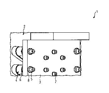
An exemplary embodiment of the invention is depicted
schematically in the single figure hereinafter and is explained
in more detail below.
BRIEF DESCIPTION OF THE DRAWING
The figure schematically shows an oblique view of a portion
of a housing 2 of a high-voltage device 1 according to
the invention, with a subassembly 3 that is electrically
insulated from the housing 2 and spaced apart from the
housing 2 via ceramic spacer elements.
DETAILED DESCRIPTION
The single figure depicts an oblique view of a portion of a
housing 2 of a high-voltage device 1 according to the invention,
with a -subassembly 3 spaced apart from the housing 2. The
subassembly 3 serves as connection or connecting element of the
high-voltage device 1, to which e.g. electrical lines, conductor
rails and/or devices, such as e.g. electrical loads and/or -
electricity generators, are connected. These can be e.g. screwed,
soldered, welded and/or clamped to the subassembly 3. The
subassembly 3 has the shape of a plate, in particular an angled
plate. An angle of 90 is formed by two portions of the plates,
each portion being in parallelepipedal form. The angled portion
of the plate points away from the housing 2, in particular
perpendicularly away from the adjacent housing surface, the other
portion of the plate being arranged parallel to the adjacent
housing surface.
CA 3073999 2020-03-30
86015203
9
The subassembly 3 spaced apart from the housing 2 is e.g. made
of steel, copper and/or coated with nickel. For reasons of cost,
cheaper materials such as e.g. aluminum and/or cast iron can
also be used. The housing 2 is made of a metal, e.g. steel, cast
iron, copper and/or aluminum. The housing *2 and the subassembly
3 are each in electrically conductive and thermally conductive.
form. The small surface of the subassembly 3 means that the
subassembly 3 emits little heat directly to the environment,
e.g. the ambient air. The large surface of the housing 2 means
that it is capable of emitting large amounts of thermal energy
to the surroundings or environment, and can therefore serve as
a cold surface.
The high-voltage device 1 according to the invention is e.g. an
instrument transformer, in particular a current transformer for
measuring currents in high-voltage lines. An insulator, e.g. a
ribbed, columnar ceramic and/or silicone insulator, which serves
as support and is not depicted in the figure for the sake of
simplicity, has a housing 2 arranged on it. The housing 2 is
e.g. spherical or pot-shaped, with a substantially circular or
quadrangular bottom. Opposite sides each have a subassembly 3
arranged on them, spaced apart from the housing 2, e.g. with a
connected overhead line. The high-voltage device 1 according to
the invention is e.g. electrically connected between the high-
voltage line in order to measure the current via the high-voltage
line. Voltages of up to 1200 kV and currents of a few thousand
amps may be present on the high-voltage device 1 according to
the invention, or can flow via the high-voltage device 1
according to the invention, in this case.
CA 3073999 2020-03-30
86015203
= 10
To measure high currents, in particular, there are e.g. coils
arranged in the housing 2 around a conductor, which are able to
be used to measure the current in the line, in particular
inductively. The conductor in the housing 2, which is not
depicted in the figure for the sake of simplicity, is
electrically connected to the subassembly 3 via electrical
contact-connection elements 7. E.g. screws and/or bolts, e.g.
made of copper and/or steel, and/or in particular weld joints,
electrically insulated from the housing 2, can be routed through
the housing 2 from inside to outside and can electrically connect
the conductor to the subassembly 3. In the figure, in exemplary
fashion, six screws as electrical contact-connection elements 7
are arranged in the plate-shaped portion of the subassembly 3
that is arranged parallel to the housing 2, i.e. are screwed
and/or routed through the plate, and electrically insulated from
the housing, routed through the housing 2 from outside to inside
and electrically connected to the conductor in the housing 2.
The subassembly 3 electrically insulated from the housing 2 is
connected to the housing 2 in mechanically robust fashion via
securing means 5, i.e. e.g. is screwed to the housing 2. In the
exemplary embodiment of the figure, there is provision on the
housing 2 for bushes 4 having e.g. internal threads in which the
screws 5 are screwed to secure the subassembly 3. Four screws 5,
two on the left-hand side of the subassembly 3 and two on the
right-hand side of the subassembly 3, are used to mechanically
secure the subassembly 3 to the housing 2. In order to prevent
electrical contact between the screws 5 and the subassembly 3,
i.e. to provide electrical insulation of the subassembly 3 from
the housing 2, e.g. insulting means 8, in particular in the form
CA 3073999 2020-03-30
86015203
11
of plastic washers, are arranged between the screw heads on the
subassembly 3 and the subassembly 3.
To provide electrical insulation, ceramic spacer elements 6 are
arranged between the housing 2 and the subassembly 3. The spacer
elements 6 can likewise be produced in the form of circular
washers, or produced in the form of hollow cylindrical sleeves.
In particular circular, continuous openings along the central
axis of the spacer elements 6 allow the screws 5 to be passed
through the spacer elements 6, i.e. the screws 5 are passed
through the spacer elements 6 and the spacer elements 6
physically encompass a region of the screws 5. The thickness or
height of the spacer elements 6 and of the bushes 4 together
determine the distance of the subassembly 3 from the housing 2.
On the side of the subassembly 3 facing the housing 2, the spacer
elements 6 electrically insulate the subassembly 3 from the
housing 2. On the side of the subassembly 3 away from the housing
2, the insulating means 8, in particular in the form of plastic
washers, electrically insulate the subassembly 3 from the housing
2 and the screws 5 from the subassembly 3.
To electrically insulate the screws 5 in the region of the
passage through the subassembly 3 from the subassembly 3, the
screws 5 can have an insulating coating, e.g. comprising Teflon,
and/or the passage has a substantially larger diameter than the
screw shank and the screws 5 are routed centrally through the
passage, and/or the passage has an insulating coating, e.g.
lacquer, and/or the ceramic spacer elements 6 have at least two
diameters, one larger and one smaller diameter, than the passage,
the spacer elements 6 protruding into or through the passage
with the smaller diameter or in the tapered region. This allows
CA 3073999 2020-03-30
86015203
12
good electrical insulation between the subassembly 3 and the
housing 2 via the ceramic spacer elements 6.
The contact surface, in particular the bearing surface, of the
subassembly 3 on the spacer elements 6, and the contact surface,
in particular the bearing surface, of the spacer elements 6 on
the housing 2 or the bushes 4 of the housing 2, provide good
thermal conduction. Heat produced on or in the subassembly 3
e.g. by large currents in the region of a few thousand amps and
the contact resistances and/or the conduction resistance of the
subassembly 3 is transferred to the housing 2 via the thermally
conductive ceramic spacer elements 6. The large outer surface of
the housing 2 effectively emits the heat to the environment. As
a result, standard values for the maximum temperature of the
connections 3 of the high-voltage device I are achievable for
very large currents.
The exemplary embodiments described above can be combined with
one another and/or can be combined with the prior art. As such,
there can be provision for precisely one ceramic spacer element
6, or there can be provision for multiple ceramic spacer elements
6. The ceramic spacer elements 6 are e.g. made of an aluminum
oxide, silicon carbide, boron nitride or aluminum nitride
ceramic. It is also possible for other ceramics to be used,. in
particular having a high specific electrical resistance and a
high thermal conductivity. The insulating means 8 can consist of
plastic washers or likewise electrically insulating ceramic and
can act analogously to the ceramic spacer elements 6. There can
be provision for bushes 4, or it is possible for securing means
5, in particular screws, to be introduced or screwed directly
into the housing wall. The subassembly 3 can be angled, or e.g.
CA 3073999 2020-03-30
86015203
13
in shallow plate-shaped form without angles, in particular with
a rectangular, round or elliptical base. High-voltage devices 1
can be e.g. current transformers, voltage transformers, combined
instrument transformers, instrument transformers for gas-
insulated switchgear, optical transformers and/or high-voltage
switches.
CA 3073999 2020-03-30
86015203
14
List of reference signs
1 High-voltage device, in particular instrument transformer
2 Housing
3 Electrically insulated subassembly
4 Bush
Securing means, in particular screw
6 Ceramic spacer element, in particular ceramic disk
7 Electrical contact-connection element into the housing, in
particular screw
8 Insulating means, in particular plastic washers
=
=
CA 3073999 2020-03-30