Note: Descriptions are shown in the official language in which they were submitted.
CA 03075163 2020-03-06
WO 2019/054995 PCMJS2017/051290
Quantum Error Correction
Field
The present application relates to hardware for error correction in quantum
computers.
More particularly, the present application relates to a classical processing
array for
determining errors in a quantum computer.
Background
Quantum computers are computing devices that exploit quantum superposition and
io entanglement to solve certain types of problem faster than a classical
computer. The
building blocks of a quantum computer are qubits. Qubits are two level systems
whose
state can be in a superposition of its two states, rather than just in either
of the two
states as is the case for a classical bit.
Quantum algorithms are algorithms that run on quantum computers. During the
execution of these algorithms on a quantum computer, errors can be introduced
from a
number of sources including decoherence and noise. Due to the no-cloning
theorem,
classical error detection and correction techniques involving creating
multiple copies of
a state are unsuitable. Instead, quantum error detection and correction
techniques
involve entangling qubits with a number of other qubits, and performing
measurements on a subset of the entangled qubits in order to identify when an
error
has occurred.
Summary
In general, in some aspects, the subject matter of the present disclosure may
be
embodied in an apparatus comprising: an array of processing cores, each
processing
core comprising: a processor on a first chip; and a processor cache on the
first chip; and
a bus for interconnecting neighbouring processing cores in the array of
processing
cores; wherein each processing core includes: control code which, when
executed by the
processor, causes the processor to access a processor cache of at least one
neighbouring
processing core
Implementations of the methods may include one or more of the following
features. For example, in some implementations, the control code is stored in
the
processor cache.
-1-
CA 03075163 2020-03-06
WO 2019/054995 PCT/US2017/051290
In some implementations, the each processor cache comprises: first-level
processor
cache; and second-level processor cache, wherein data passes between the
processor
and the second-level processor cache via the first-level cache.
In some implementations, the control code is stored in the first level
processor cache.
In some implementations, the controller code comprises machine code.
io In some implementations the controller code, when executed by the
processor, causes
the processor to access the second-level processor cache of the at least one
neighbouring processor core.
In some implementations, the processor cache comprises one or more buffers
configured to store data accessed from the at least one neighbouring
processing core.
In some implementations, the data accessed from the at least one neighbouring
processing core is cyclically written to one or more of the buffers.
In some implementations, each processing core is arranged to receive a
respective set of
measurement data, to store the set of measurement data in the processor cache
and to
process the set of measurement data.
In some implementations, instructions for processing the measurement data are
stored
in the processor cache.
In some implementations, to process the set of measurement data, the
processing core
is configured to perform quantum error correction.
In some implementations, the quantum error correction comprises implementing a
surface code.
In some implementations, to process the set of measurement data, the
processing core
is configured not to use random access memory.
- 2 -
CA 03075163 2020-03-06
WO 2019/054995 PCT/US2017/051290
In some implementations, the processor core further comprises one or more
additional
processors.
Further aspects of the present disclosure may be embodied in a system
comprising: a
.. first classical computing layer comprising an array of processing cores
according to any
preceding implementation; and a quantum computing layer comprising an array of
quantum devices configured to implement a quantum computing algorithm, wherein
the classical processing layer is configured to: receive measurement data from
the
quantum computing layer; and determine one or more errors in the quantum
io computing algorithm performed by the quantum computing layer using the
received
measurement data.
Further aspects of the present disclosure may be embodied in a system
comprising: a
first classical computing layer comprising an array of processing cores, each
processing
core comprising: a processor; and a processor cache ;and a bus for
interconnecting
neighbouring processing cores in the array of processing cores; wherein each
processing core includes: control code which, when executed by the processor,
causes
the processor to access a processor cache of at least one neighbouring
processing core;
a quantum computing layer comprising an array of quantum devices configured to
implement a quantum computing algorithm, wherein the classical processing
layer is
configured to: receive measurement data from the quantum computing layer; and
determine one or more errors in the quantum computing algorithm performed by
the
quantum computing layer using the received measurement data.
In some implementations, the system further comprises a control layer
comprising an
array of field-programmable gated arrays configured to: receive physical
measurements
from the quantum computing layer; convert the physical measurements to
measurement data; and output the measurement data to the first classical
computing
layer.
In some implementations, the control layer is further configured to: receive
quantum
error correction instructions; and in response to receiving the quantum error
correction
instructions, cause the implementation of one or more qubit rotations on the
quantum
computing layer.
- 3 -
In some implementations, the system further comprises a second classical
processing layer
configured to: receive one or more determined errors in the quantum computing
algorithm from
the first classical computing layer; and determine one or more quantum error
correction
instructions from the one or more determined errors.
In some implementations, the second processing layer is further configured to
cause the one or
more quantum error correction instructions to be implemented in the quantum
computing
layer.
io In some implementations, the second processing layer is configured to
implement a surface code
to determine the one or more quantum error correction instructions.
In some implementations, each processing core in the first classical
processing layer receives
measurements from a local patch of quantum devices in the quantum computing
layer.
In another aspect, there is provided an apparatus comprising: an array of
processing cores, each
processing core comprising: a processor on a first chip; and a processor cache
on the first chip;
and a bus for interconnecting neighbouring processing cores in the array of
processing cores;
wherein each processing core includes: control code which, when executed by
the processor,
causes the processor to access a processor cache of at least one neighbouring
processing core,
and wherein the array of processing cores is configured to: receive
measurement data from a
quantum computing layer comprising an array of quantum devices executing a
quantum
algorithm comprising a surface code, each processing core configured to
receive measurements
from a local patch of quantum devices in the array of quantum devices, wherein
neighbouring
local patches of quantum devices in the array of quantum devices are
associated with
neighbouring processor cores; convert the measurement data into a plurality of
detection
events; match a detection event to another detection event to form a matched
pair, the matching
comprising: attempting, by a processor core associated with the local patch
containing the
detection event, to match the detection event to a detection event in the same
local patch; and if
the processor core is unable to match a detection event to another detection
event in the same
local patch, accessing the processor cache of a neighbouring processor core
and attempting to
match the detection event to a detection event in a neighbouring local patch
corresponding to
the neighbouring processor core, and determine one or more errors in the
quantum computing
algorithm performed by the quantum computing layer using the matched pair.
- 4 -
Date Recue/Date Received 2021-09-17
In another aspect, there is provided a system comprising: a first classical
computing layer
comprising an array of processing cores as disclosed above; and the quantum
computing layer
comprising an array of quantum devices configured to implement a quantum
computing
algorithm.
In another aspect, there is provided a system comprising: a first classical
computing layer
comprising an array of processing cores, each processing core comprising: a
processor; and a
processor cache; and a bus for interconnecting neighbouring processing cores
in the array of
processing cores; wherein each processing core includes control code which,
when executed by
io the processor, causes the processor to access a processor cache of at
least one neighbouring
processing core, and a quantum computing layer comprising an array of quantum
devices
configured to implement a quantum computing algorithm, the quantum computing
algorithm
comprising a surface code, wherein the classical processing layer is
configured to: receive
measurement data from the quantum computing layer, each processing core
configured to
/5 receive measurements from a local patch of quantum devices in the array
of quantum devices,
wherein neighbouring local patches of quantum devices in the array of quantum
devices are
associated with neighbouring processor cores; convert the measurement data
into a plurality of
detection events; match a detection event to another detection event to form a
matched pair, the
matching comprising: attempting, by a processor core associated with the local
patch containing
20 the detection event, to match the detection event to a detection event
in the same local patch;
and if the processor core is unable to match a detection event to another
detection event in the
same local patch, accessing the processor cache of a neighbouring processor
core and attempting
to match the detection event to a detection event in a neighbouring local
patch corresponding to
the neighbouring processor core; and determine one or more errors in the
quantum computing
25 algorithm performed by the quantum computing layer using the matched
pair.
In another aspect, there is provided a computer-implemented method comprising:
receiving, by
a classical processing layer comprising an array of processing cores,
measurement data from a
quantum computing layer, wherein each processing core in the array of
processing cores
30 receives measurement data from a local patch of quantum devices in the
quantum computing
layer; identifying, by the classical processing layer, a plurality of
detection events in the
measurement data; matching, by the classical processing layer, a detection
event to another
detection event to form a matched pair, the matching comprising: i)
attempting, by a processor
core associated with the local patch containing the detection event, to match
the detection event
- 4a -
Date Recue/Date Received 2021-09-17
to a detection event in the same local patch, and ii) if the processor core is
unable to match a
detection event to another detection event in the same local patch, accessing
the processor cache
of a neighbouring processor core and attempting to match the detection event
to a detection
event in a neighbouring local patch corresponding to the neighbouring
processor core; and
determine one or more errors in the quantum computing algorithm performed by
the quantum
computing layer using the matched pair.
List of Figures
io Figure 1 shows a schematic example of an embodiment of a quantum
computer;
Figure 2 shows an example of a processing core for a classical processing
layer;
Figure 3 shows an example of a part of a classical processing array according
to an embodiment;
Figure 4 shows an example of multiple processor cores;
Figure 5 shows a further example of multiple processor cores;
/5 Figure 6 shows a schematic example of a further embodiment of a quantum
computer; and
Figure 7 shows a schematic example of processes performed in a quantum
computer according
to an embodiment.
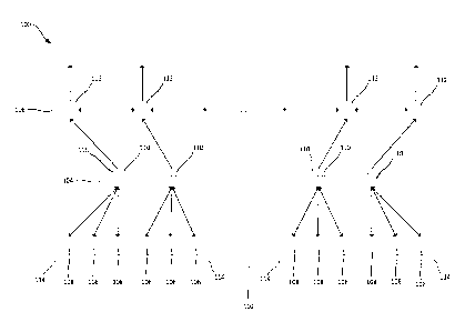
Figure 8 shows an example three-dimensional data structure of an array
representing a given
local patch that is cyclically written to the processor cache of the processor
core associated with
20 that local patch.
Detailed description
Figure 1 illustrates a schematic example of an embodiment of a quantum
computer mo.
- 4b -
Date Recue/Date Received 2021-09-17
CA 03075163 2020-03-06
WO 2019/054995 PCT/US2017/051290
The quantum computer 100 comprises a quantum computing layer 102, a control
layer
104 and a classical processing layerro6.
The quantum computing layer 102 comprises an array of quantum devices or
qubits
io8 configured to perform a quantum computing algorithm. The quantum devices
or
qubits 108 comprise a mixture of data qubits and syndrome (or measurement)
qubits.
The quantum computing layer 102 further comprises a plurality of quantum gates
(not
shown) for performing operations on the qubits 108. In some embodiments, the
quantum computing layer is in the form of a two-dimensional array of quantum
devices
108.
The quantum devices or qubits 108 can, for example, be superconducting qubits.
The
quantum computing layer 102 is kept at a sufficiently low temperature to
maintain
coherence between qubits throughout the execution of the quantum algorithm
(for
example, below 4.2K). In embodiments where superconducting qubits are used,
the
temperature is kept below the superconducting critical temperature. Herein,
for the
term "qubit" and "quantum device" will be used interchangeably.
A control layer 104 comprising a plurality of control devices no is interposed
between
the quantum computing layer 102 and the classical processing layer 106. The
control
devices 110 receive raw measurement data from qubits 108 in the quantum
computing
layer 102 and convert them into binary measurement data for use in the
classical
processing layer 106. The control devices no can, in some embodiments, also
issue
instructions to the quantum devices 108, for example to instruct a quantum
gate (not
shown) to perform a qubit rotation. In some embodiments, each control device
110 is
connected to around six quantum devices 108. The control devices no are, in
some
embodiments, Field Programmable Gated Arrays (FPGAs).
The classical processing layer 106 (herein also referred to as "the first
classical
processing layer") comprises an array of processing cores 112. The processing
cores 112
are described in further detail below in relation to Figure 2. The classical
processing
layer 106 is coupled to the quantum computing layer 102 via the control layer
104.
Processing cores 112 in the classical computing layer 106 are associated with
local
patches 114 of qubits 108. A local patch 114 comprises a plurality of qubits
108 grouped
together. In some embodiments, the patch size is around one hundred qubits.
Processing cores 112 in the classical processing layer 106 are coupled to
neighbouring
- 5 -
CA 03075163 2020-03-06
WO 2019/054995
PCT/US2017/051290
processing cores 112 in the classical processing layer 106. This can allow the
processing
cores 112 to exchange data with their neighbouring cores. In some embodiments,
the
processing cores 112 form a two-dimensional array of processing cores 112
within the
classical processing layer 106.
The classical processing cores 112 are provided with dedicated assembly
instructions,
that, when executed by a processor in the processor core, cause the processor
to access
the processor cache of a neighbouring core. This can result in low latency
communication between neighbouring cores, as a complex memory controller is
not
io needed.
In use, the quantum computing layer 102 executes a quantum computing
algorithm.
Syndrome qubits in the quantum computing layer 102 interact with their
neighbouring
data qubits to produce raw measurement data. The raw measurement data is fed
into
the control devices 110 of the control layer 104. The control devices 110
convert the raw
measurement data into binary measurement data and stream the binary
measurement
data into the processing cores 112 of the classical processing layer 106.
The classical processing layer 106 converts the binary measurement data from
the
control layer 104 into parities of the quantum states of qubits 108 in the
quantum
computing layer 102 that were measured. These parities are then processed by
the
classical processing layer 106 to determine any quantum errors and/or the
required
corrected parities for the quantum devices 108 in the quantum computing layer
102.
The determined corrections can then be processed further to determine the
required
corrective action.
Figure 2 shows an example of a processing core for the classical computing
layer. Each
processor core 112 of the classical processing layer 106 comprises a processor
116, one
or more processor caches 118 and busses 120 to nearest-neighbour processing
cores in
the classical processing layer 106. Processing cores 112 are provided on a
chip.
The busses 120 interconnect neighbouring processing cores 112 in the array of
processing cores in the classical processing layer 106. The busses 120 allow a
processor
116 to access the processor caches 118 of its nearest-neighbour processing
cores 112 to
obtain measurement data from local patches 114 of quantum devices 108
associated
with neighbouring processing cores 112. Each processing core 112 is provided
with
- 6 -
CA 03075163 2020-03-06
WO 2019/054995 PCT/US2017/051290
control code 126 which, when executed by the processor 116, cause the
processor 116 to
access the processor cache ii8 of at least one neighbouring processing core
112. The
control code 126 is stored within the processor cache 118 to speed up access
of the code
by the processor 116. In some embodiments, the control code is in the form of
machine
.. code or assembly code.
The processor core 112 can be constructed to recognise the control code (for
example in
the form of assembly code) that can trigger direct access of the processor
cache 118 of at
least one neighbouring processor cores 112. For example, the processor core
112 can
io have an input/output circuitry that directly accesses the processor
cache 118 of at least
one or more similarly constructed processor cores. The processor core 112 is
constructed to process corresponding assembly code instructions that are
specific to the
processing core to cause the direct access to the processing cache ii8 of one
or more
neighbouring processor cores 112. Any appropriate processor fabrication
techniques
can be used to implement such circuity.
The processor cores 112 can access data from processing cores 112 further away
than
their nearest neighbour processing cores. For example, next nearest or next-
next
nearest neighbour processing cores 112 can be accessed. This additional
communication can be achieved in a number of ways. For example, the
information at a
particular coordinate can be requested by sending a request in the direction
of that
coordinate until it reaches the processor core 112 in charge of that
coordinate. This
processor core 112 can send the requested information back to the requester.
Another
example is having additional assembly level instructions for more than just
the nearest
four cores stored in the processing core.
The processor cache ii8 further stores instructions for processing measurement
data
received by the processing core. These instructions comprise a quantum error
correction and/or determination algorithm. In some examples the quantum error
correction algorithm comprises a surface code, such as a Toric code for
example. An
example of a surface code is provided in "Towards practical classical
processing for
the surface code: timing analysis" by Fowler et al.
[https://doi.org/io.no3/PhysRevLett.108.180501].
- 7 -
CA 03075163 2020-03-06
WO 2019/054995 PCT/US2017/051290
In some embodiments, the processor cache comprises an Li cache 122 (herein
also
referred to as "a first-level cache") and an L2 cache 124 (herein also
referred to as "a
second-level cache").
The processor cores 112, constructed as described above, can process the
instructions
that trigger direct communication among the cache layers. In some
implementations,
the Li cache is used to store the state of a quantum error correction process,
and the L2
cache stores the instructions that implement quantum error correction process.
ro The Li cache 122 comprises data 130 comprising the measurement data
currently being
processed by the processor 116.
The L2 cache 124 stores data comprising instructions 128 for performing a
quantum
error correction algorithm. The control code 126 for accessing neighbouring
processing
cores 112 is also stored in the L2 cache 124. Low level assembly instructions
132 are also
used to move the measurement data between the Li cache 122 and L2 cache 124 of
a
processing core 112. In some embodiments the low level assembly instructions
132 are
provided as part of the control code 126. In other embodiments, the low level
assembly
instructions 132 are provided separately.
The L2 cache 124 also stores measurement data 134 obtained from quantum
devices
108 in the local patch 114 that the processing core 112 is associated with.
Measurement
data 134 from the associated local patch 114 is fed from the quantum computing
layer
102 into the L2 cache 124 via the control layer 104. The measurement data 134
is
transferred to the processor 116 for processing via the Li cache 122 as
required.
Each L2 cache 124 further comprises receive buffers (not shown) for each of
the busses
120 of the processor core 112. The buffers are written to cyclically by the
corresponding
neighbouring processing core. The buffer can be configured to issue a "stop
bit" to let
other cores know that it is overloaded to reduce contention. The control code,
when
executed by the processor in such embodiments, can cause the processor to
access the
second-level processor cache 124 of a neighbouring processor core.
The use of the processor cache to store the algorithm instructions and
measurement
data can reduce or even remove the need for external memory, such as random
access
memory, when performing quantum error correction. This can help reduce latency
when performing the error correction algorithm.
- 8 -
CA 03075163 2020-03-06
WO 2019/054995 PCT/US2017/051290
In some embodiments, the Li cache has a memory of between 8 kB and 128 kB. In
some embodiments, the Li cache has a memory of 64 kB. In some embodiments, the
L2
cache has a memory of between 0.5 MB and 3 MB. In some embodiments, the L2
cache
has a memory of 1.5MB.
An example of a part of an array using a single processing core per local
patch is shown
in Figure 3.
/o The classical processing layer comprises an array of classical
processing cores 112. The
array comprises a plurality of motherboards 136, each comprising a processing
core
112. In the example given, only four processing cores are shown, though in
general the
array can consist of any number of processing cores 112.
A processor core 112 is located on each motherboard 136 in the array.
Processor caches
118 on neighbouring motherboards 136 are linked via the busses 120.
Each processing core 112 receives measurement data from a local patch 114 of
quantum
devices 108 in the quantum computing layer 102. Collectively the processing
cores 112
in the array cover the local patches 114 of interest in the quantum computing
layer 102.
In some embodiments, the array covers all local patches 114 in the quantum
computing
layer 102.
During execution of a quantum error correction algorithm, the buses 120 allow
a
processing core 112 to access measurement data in neighbouring processing
cores 112.
Neighbouring processing cores 112 are associated with local patches 114 in the
quantum
computing layer 102 neighbouring the local patch 114 of the processing core
112
accessing the measurement data.
Referring also to Figure 4, in some alternative embodiments, multiple
processing cores
112 are located on each motherboard 136. Each processor core 112 comprises one
or
more processors 116 and a processor cache 118. The processor cores 112 on each
motherboard 136 can exchange data via an intra-motherboard bus 138 (which in
some
embodiments can be in the form of an L3 cache). In the embodiment shown, the
motherboard 136 is provided with four processor cores 112. However, fewer or
more
processor cores 112 can be used.
- 9 -
CA 03075163 2020-03-06
WO 2019/054995 PCT/US2017/051290
In the embodiment shown, processor cores 112 on the perimeter of the
motherboard
126 each have directional busses 140 to their nearest neighbour processor
cores on
neighbouring motherboards. This can allow exchange of measurement data between
processor caches of neighbouring processor cores on different motherboards.
Referring also to Figure 5, an alternative to having each of the perimeter
processor
cores 112 having directional busses to nearest neighbour processor core on
neighbouring motherboards is to have common directional busses 140 for the
/o perimeter processors that are used as a shared resource. In this
embodiment, the
common directional busses 140 exchange data between processor caches on
neighbouring motherboards. The common directional busses 130 can be connected
with the intra-motherboard bus 138, allowing data from the caches of
neighbouring
motherboard processor cores to be used by any of the processor cores 112 on
the
motherboard 126.
Referring also to Figure 6, additional processing can be provided in a second
classical
processing layer 134. The second classical processing layer comprises an array
of
second layer processing cores 136. The second layer processing cores 136 in
the second
classical processing layer 134 use the corrected parities and/or identified
errors output
by the classical processing layer io6 to determine instructions for correcting
the
identified quantum errors. The determined instructions 146 are transmitted to
the
control layer 104, which converts them to control signals and applies them to
the
quantum devices io8 in the quantum computing layer 102, thereby correcting the
identified errors.
Typically the second processing layer 142 has fewer second layer processing
cores 144
than the first classical processing layer io6 has processing cores 112. In
some
embodiments the second classical processing layer 142 has up to a factor of
loo fewer
processing cores. The second classical processing layer 142 can also provide
global
quantum algorithm control.
The system described above is particularly suited for implementing a surface
code to
determine and correct quantum errors. An example of such a surface code is the
Toric
code.
- 10 -
CA 03075163 2020-03-06
WO 2019/054995 PCT/US2017/051290
In use, the quantum computing layer executes a quantum algorithm with a
surface code
being used for error correction. The surface code can be visualized as a large
checker-
board. Each square represents a qubit. White squares correspond to qubits
being used
to store data, and are referred to as data qubits. Black squares correspond to
qubits
being used to check for errors in their neighbouring four data qubits, and are
referred
to as measurement or syndrome qubits. Computation is achieved by turning on
and off
regions of the surface code. Physically, this involves causing the measurement
qubits to
cease interacting with data qubits within specific regions of the quantum
computing
layer.
In this situation, the quantum algorithm can be visualized as a three-
dimensional
geometric structure, or array, with time running vertically. The execution of
the
algorithm can be visualized as operating in a two dimensional (for a one-
dimensional
array of qubits) or three dimensional (for a two-dimensional array of qubits)
data
structure, sometimes called the "space-time" or "volume". This data structure
can be
constructed from regular building blocks, which are referred to herein as
"plumbing
pieces". A stream of these plumbing pieces can be fed into control hardware
and
expanded into collections of physical quantum gates. These physical quantum
gates can
be converted into hardware-specific control signals for controlling the
progress of the
.. quantum algorithm.
Figure 7 illustrates an example of processes performed in a quantum computer
during
execution of a quantum computing algorithm. During execution of the quantum
algorithm, measurement qubits interact with their neighbouring data qubits in
parallel
within the quantum computing layer 102, and perform measurements of the data
qubit
quantum states 148. In some embodiments, during every cycle of checking a
number of
binary measurements equal to half the number of qubits in the quantum computer
is
generated. Rounds of measurements are performed sequentially in time.
The physical measurements of the data qubits by the measurement qubits are
passed to
the control layer 104 as readout signals 150. In the control layer, the
readout signals
150 are converted into measurement data 152. The measurement data 152 are then
transmitted to the classical processing cores in the first classical
processing layer io6
.. corresponding to the local patch of quantum devices from which the
measurement data
152 originated.
- 11 -
CA 03075163 2020-03-06
WO 2019/054995 PCT/US2017/051290
The first classical processing layer receives the measurement data and
processes it to
determine any errors in the execution of the quantum algorithm.
.. The first step is to convert the measurements to detection events. In some
embodiments this is achieved by comparing each measurement at a location in
the
quantum computing layer with the previous measurement at the same location.
When
the measurement at a location differs from the previous measurement at that
location a
detection event is recorded at that location.
In the surface code, detection events correspond to the end points of chains
of errors in
the quantum algorithm. To determine possible error corresponding to the
detection
events, detection events are matched to each other to form pairs, or are
matched to a
boundary of the qubit array.
Matching of the detection events is performed in the first classical
processing layer 106.
Each classical processor core stores layered representations of the potential
detection
events that can occur in its corresponding local patch. In some embodiments,
the
layered representations comprise potential detection events that can occur
during a
.. round of error detection at stages of the quantum algorithm. Emanating from
the
potential detection events in each layer are a set of weighted lines
connecting the
detection event to other potential detection events. The weight of each line
is
representative of the probability of detection events at each end of the line
occurring
together as the result of an error. In some embodiments, the lines are
weighted such
that higher probability lines have a lower weight than lower probability
lines.
The layered representation is pre-determined based on knowledge of the quantum
algorithm and the possible errors that can occur during its execution. The
layered
representation is chosen such that the representation for each local patch
fits into the
.. processor cache of the corresponding processor core in the first classical
computing
layer.
As the quantum algorithm progresses, the layered representations are used to
construct
an array in each of the classical processing cores representing the progress
of the
algorithm. Horizontal slices of the array correspond to rounds of error
detection
measurements, as described hereinafter. The array representing a given local
patch is
- 12 -
CA 03075163 2020-03-06
WO 2019/054995 PCT/US2017/051290
cyclically written to the processor cache of the processor core associated
with that local
patch. Referring to Figure 8, an example of such an array 156 will now be
described. In
the figure, time runs cyclically from left to right. As detection events 158
are determined
in the array 156, the processor core attempts to match them to other
determined
detection events in the array using minimum weight perfect matching. The array
is
constructed from the relevant layers 160 of the layered representation (only
some of
which are labelled in Figure 8) that correspond to the stages of the quantum
algorithm
that the quantum computer has passed through.
io The instructions for each processor core to perform the minimum weight
perfect
matching are stored in the processor cache of that processor core. This allows
for fast
execution of the matching algorithm, as no external memory needs to be
accessed.
Matching the detection events results in a list of errors 162 that may have
occurred in
the execution of the quantum algorithm.
During matching of the detection events by a processor core, the processor
core may
require data relating to detection events in a local patch of devices
neighbouring its own
local patch. For example, if the processor is unable to match a detection
event to
another detection event in its local patch, it may be able to match it to a
detection event
in a neighbouring local patch. In these situations, the processor core can
access the
processor cache of a neighbouring processor core via the directional busses
between
them, as described above.
Using the matched detection events, the errors that resulted in them can be
determined. The corresponding parity corrections can be determined from the
errors,
and are inserted into a representation of the space-time of the quantum
algorithm.
This can, in some embodiments, be a layered structure storing physical qubit
level Pauli
frame 154 information.
In some embodiments, the error list 162 is in the form of correlation surface
parities.
After matching, corrections are inserted in space-time in a classical
simulation of the
quantum computer, as described above. These corrections can be propagated
forward
in time through the quantum gates (which can be done efficiently) to determine
the
true value of the physical measurement results. Parities of corrected
measurement
results on correlation surfaces are then sent for higher-level processing.
- 13 -
CA 03075163 2020-03-06
WO 2019/054995 PCT/US2017/051290
In some embodiments, the corrected parities are passed to the second classical
processing layer 142 for higher-level processing. The second classical
processing layer
142 is used to determine future logical gates required in order to correct the
quantum
algorithm. The corrected parities 162 are converted into logical measurement
results
and logical by-product operators 164. The set of all logical by-product
operators is
called the logical Pauli frame. Given the logical Pauli frame and logical
measurement
results, the necessary corrective action to correct the quantum algorithm can
be
determined. The logical measurements and logical Pauli frame 164 comprise
values of
measurements of logical qubits, with results being o or 1, and the way in
which
/o unmeasured logical qubits differ from their ideal values. The
differences can be
represented as one of the I, X, Y, Z operators, each being a 2X2 matrix.
The second classical processing layer also provides global quantum algorithm
control.
Global quantum algorithm control can, in some embodiments, be implemented
using
the following features.
Logical measurement dependant logical Clifford+T circuit module 166. Quantum
circuits are comprised of quantum gates. An example of such a type of gate is
Clifford
gates, which comprise initialization, measurement, I, X, Y, Z, CNOT, CZ, S, H
operations and combinations thereof. A further example is a T gate. Quantum
circuits
are like software, with some future gates dependant of the value of
intermediate
measurements. The Logical measurement dependant logical Clifford+T circuit
module
166 determines these logical measurement dependent future gates from the
logical
measurements. These can comprise future gates to implement the identified
error
correction determined by the first layer. Once a number of logical
measurements have
been obtained, the future gates of the quantum circuit can be determined. An
increasing number of gates get known with confidence as computation proceeds
and
more logical measurements become available. The output of this module is a
Logical
Clifford+T circuit 168.
Topological skeleton plus state distillation factories module 170. The known
part of the
algorithm determined by the Logical measurement dependant logical Clifford+T
circuit
module 166 is converted into standard structures, referred to as the
"topological
skeleton", and factories for distilling ancilla quantum states for use in the
quantum
algorithm.
- 14 -
CA 03075163 2020-03-06
WO 2019/054995 PCT/US2017/051290
Skeleton, factories, and paths from factories to skeleton module 172. Given
the
Topological skeleton plus state distillation factories determined by the
Topological
skeleton plus state distillation factories module 170, logical measurements
164 can be
used to determine which factories have succeeded in distilling an ancilla
state. The
paths required to connect these states to the topological skeleton where the
output is
needed are then determined.
Correlation surfaces module 174. The correlation surfaces are sets of
measurements
whose parities give a logical measurement result and/or generate a logical
Pauli frame
io correction. A correlation surface indicates which parity of measurement
results to
examine to determine whether a logical X and/or Z by-product operators have
been
introduced into the computation. The correlation surfaces are determined from
the
output of the Skeleton, factories, and paths from factories to skeleton module
172. The
correlation surfaces are output to the first classical computing layer 106 for
use in
determining parities from physical measurements.
Plumbing pieces module 176. The plumbing piece module converts the output of
the
Skeleton, factories, and paths from factories to skeleton module 172 into a
set of
plumbing pieces for implementing the required gates in the quantum computing
layer
102.The plumbing piece module 176 outputs plumbing pieces to the control layer
104
for implementation in the quantum computing layer 102. The control layer
converts
these to physical gate operations 178. These are then output as control pulses
180 to
gates in the quantum computing layer 102 in order to implement the quantum
algorithm with the determined corrections.
The determined corrective actions are then output by the second classical
processing
layer to the control layer 104. There, physical gates convert the determined
corrective
actions into control pulses. The control pulses are used to implement the
corrective
action on qubits in the quantum computing layer 102.
Implementations of the quantum subject matter and quantum operations described
in this specification may be implemented in suitable quantum circuitry or,
more
generally, quantum computational systems, including the structures disclosed
in this
specification and their structural equivalents, or in combinations of one or
more of
them. The term "quantum computational systems" may include, but is not limited
to,
-15 -
CA 03075163 2020-03-06
WO 2019/054995 PCT/US2017/051290
quantum computers, quantum information processing systems, quantum
cryptography
systems, or quantum simulators.
The terms quantum information and quantum data refer to information or data
that
is carried by, held or stored in quantum systems, where the smallest non-
trivial system
is a qubit, e.g., a system that defines the unit of quantum information. It is
understood
that the term "qubit" encompasses all quantum systems that may be suitably
approximated as a two-level system in the corresponding context. Such quantum
systems may include multi-level systems, e.g., with two or more levels. By way
of
example, such systems can include atoms, electrons, photons, ions or
superconducting
qubits. In many implementations the computational basis states are identified
with the
ground and first excited states, however it is understood that other setups
where the
computational states are identified with higher level excited states are
possible. It is
understood that quantum memories are devices that can store quantum data for a
long
time with high fidelity and efficiency, e.g., light-matter interfaces where
light is used for
transmission and matter for storing and preserving the quantum features of
quantum
data such as superposition or quantum coherence.
Quantum circuit elements may be used to perform quantum processing operations.
That is, the quantum circuit elements may be configured to make use of quantum-
mechanical phenomena, such as superposition and entanglement, to perform
operations on data in a non-deterministic manner. Certain quantum circuit
elements,
such as qubits, may be configured to represent and operate on information in
more
than one state simultaneously. Examples of superconducting quantum circuit
elements
that may be formed with the processes disclosed herein include circuit
elements such as
co-planar waveguides, quantum LC oscillators, qubits (e.g., flux qubits or
charge
qubits), superconducting quantum interference devices (SQUIDs) (e.g., RF-SQUID
or
DCSQUID), inductors, capacitors, transmission lines, ground planes, among
others.
In contrast, classical circuit elements generally process data in a
deterministic manner.
Classical circuit elements may be configured to collectively carry out
instructions of a
computer program by performing basic arithmetical, logical, and/or
input/output
operations on data, in which the data is represented in analogue or digital
form. In
some implementations, classical circuit elements may be used to transmit data
to
and/or receive data from the quantum circuit elements through electrical or
electromagnetic connections. Examples of classical circuit elements that may
be formed
- 16 -
with the processes disclosed herein include rapid single flux quantum (RSFQ)
devices,
reciprocal quantum logic (RQL) devices and ERSFQ devices, which are an energy-
efficient
version of RSFQ that does not use bias resistors. Other classical circuit
elements may be formed
with the processes disclosed herein as well.
During operation of a quantum computational system that uses superconducting
quantum
circuit elements and/or superconducting classical circuit elements, such as
the circuit elements
described herein, the superconducting circuit elements are cooled down within
a cryostat to
temperatures that allow a superconductor material to exhibit superconducting
properties.
While this specification contains many specific implementation details, these
should not be
construed as limitations, but rather as descriptions of features that may be
specific to particular
implementations. Certain features that are described in this specification in
the context of
separate implementations can also be implemented in combination in a single
implementation.
Conversely, various features that are described in the context of a single
implementation can
also be implemented in multiple implementations separately or in any suitable
sub-
combination. Moreover, although features may be described above as acting in
certain
combinations, one or more features from a combination can in some cases be
excised from the
combination, and the combination may be directed to a sub-combination or
variation of a sub-
combination.
Similarly, while operations are depicted in the drawings in a particular
order, this should not be
understood as requiring that such operations be performed in the particular
order shown or in
sequential order, or that all illustrated operations be performed, to achieve
desirable results. In
certain circumstances, multitasking and parallel processing may be
advantageous. Moreover,
the separation of various components in the implementations described above
should not be
understood as requiring such separation in all implementations.
A number of implementations have been described. Nevertheless, it will be
understood that
various modifications may be made. The invention, rather, is defined by the
claims.
- 17 -
Date Recue/Date Received 2021-09-17