Note: Descriptions are shown in the official language in which they were submitted.
PARAMETRIC AMPLIFIER SYSTEM
RELATED APPLICATIONS
[0001] This application claims priority from U.S. Patent Application
Serial
No. 15/799017, filed 31 October 2017, which issued as U.S. Patent No.
10,491,178.
TECHNICAL FIELD
[0002] This disclosure relates generally to classical and quantum
computing systems, and
more specifically to a parametric amplifier system.
BACKGROUND
[0003] A parametric oscillator is a driven harmonic oscillator in which
the oscillations
are driven by varying some parameter of the system at some frequency,
typically different from
the natural frequency of the oscillator. A parametric oscillator can amplify a
signal as
a parametric amplifier, such as when operated at pump levels below
oscillation. A typical
parametric amplifier can exhibit much lower noise than an ordinary amplifier
based on a gain
device like a transistor or vacuum tube based on varying a reactance instead
of resistance. An
example of a parametric oscillator is a varactor parametric amplifier that
operates as a low-noise
amplifier in the radio and microwave frequency range. A varactor parametric
amplifier can
provide non-linear adjustment to the reactance of a given microwave signal via
a varactor diode.
Applications that require a parametric amplifier can require both high
bandwidth and high gain,
which can sometimes result in trade-offs in a given parametric amplifier
design.
SUMMARY
[0004] One example includes a parametric amplifier system. The system
includes an
input/output (I/O) transmission line to propagate a signal tone. The system
also includes a non-
linearity circuit comprising at least one Josephson junction to provide at
least one inductive path
of the signal tone in parallel with the at least one Josephson junction. The
system further
includes an impedance matching network coupled to the I/O transmission line to
provide
1
CA 3076182 2021-08-13
CA 03076182 2020-03-10
WO 2019/089141 PCT/1JS2018/051076
impedance matching of the tone signal between the I/O transmission line and
the non-linearity
element.
[0005] Another example includes a parametric amplifier system. The system
includes an
I/0 transmission line to propagate a signal tone and at least one impedance
matching element
coupled to the I/0 transmission line to provide a frequency pole associated
with the signal tone.
The system also includes a non-linearity circuit comprising at least one
Josephson junction to
provide at least one inductive path of the signal tone in parallel with the at
least one Josephson
junction.
[0006] Another example includes a parametric amplifier system. The system
includes an
1/0 transmission line to propagate a signal tone and at least one impedance
matching element
coupled to the I/0 transmission line to provide a frequency pole associated
with the signal tone.
The system also includes a non-linearity circuit comprising a plurality of RF
superconducting
quantum interference devices (SQUIDs) arranged in alternating orientations in
an array between
a first terminal of the non-linearity circuit and a second terminal of the non-
linearity circuit to
provide at least one inductive path of the signal tone.
BRIEF DESCRIPTION OF THE DRAWINGS
[0007] FIG. 1 illustrates an example of a parametric amplifier system.
[0008] FIG. 2 illustrates another example of a parametric amplifier
system.
[0009] FIG. 3 illustrates an example of a non-linearity circuit.
DETAILED DESCRIPTION
[0010] This disclosure relates generally to classical and quantum
computing systems, and
more specifically to a parametric amplifier system. The parametric amplifier
system can be
implemented in any of a variety of classical and quantum computer systems that
may require
amplification of a signal tone, such as for a state-readout of a qubit. The
parametric amplifier
system can include an input/output (I/O) transmission line on which a high-
frequency signal tone
(e.g., having a center frequency of approximately 7.5 GHz) can propagate. As
an example, the
2
CA 03076182 2020-03-10
WO 2019/089141 PCT/1JS2018/051076
1/0 transmission line can correspond to both an input and output associated
with the signal tone,
such that the amplified output signal tone can be reflected back to the I/O
transmission line and
can be separated from the input signal tone at the I/O transmission line
(e.g., via a circulator). As
a result, the output signal tone can be provided from the I/0 transmission
line and processed
(e.g., via an analog-to-digital converter (ADC)).
[0011] The parametric amplifier also includes at least one impedance
matching element
to provide a respective at least one frequency pole with respect to the signal
tone. As an
example, each of the impedance matching element(s) can be configured as a
resonator coupled to
the I/O transmission line, and can each be separated by a reactive circuit
element (e.g., a
capacitor or an inductor). The parametric amplifier further includes a non-
linearity circuit that is
configured to provide the amplification of the signal tone. As an example, the
non-linearity
circuit can include at least one Josephson junction that is arranged in
parallel with at least one
inductive path of the signal tone. For example, the non-linearity circuit can
include a plurality of
RF superconducting quantum interference devices (SQUIDs) that are arranged in
an alternating
series arrangement. Each of the R F SQUIDs can include a Josephson junction
and a pair of
inductors that form an inductive path in parallel with the respective
Josephson junction. For
example, the arrangement of the RF SQUIDs can include two inductive paths in
parallel, such
that two series RF SQUID arrangements can be provided in parallel between
respective terminals
of the non-linearity circuit As a result, the parametric amplifier can achieve
sufficient gain (e.g.,
at least approximately 20 dB) over a large bandwidth (e.g., at least
approximately 1 GHz) with a
high saturation power (e.g., approximately -90 dB).
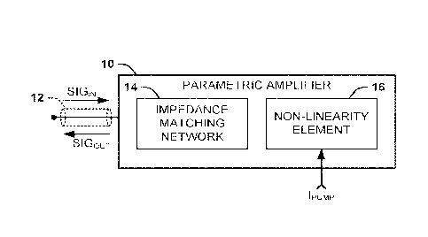
[0012] FIG. I illustrates an example of a parametric amplifier system 10.
The parametric
amplifier system 10 can be implemented in any of a variety of classical and
quantum computer
systems that may require amplification of a signal tone, such as for a state-
readout of a qubit.
[0013] The parametric amplifier system 10 includes an input/output (I/0)
transmission
line 12 on which a high-frequency signal tone, demonstrated in the example of
FIG. 1 as a signal
SIG, can propagate. As an example, the signal tone SIG can have a frequency in
a range of
frequencies encompassing a frequency band of at least approximately 1.6 GHz
that can be
3
CA 03076182 2020-03-10
WO 2019/089141 PCT/1JS2018/051076
centered at approximately 7.5 GHz. In the example of FIG. 1, the I/O
transmission line 12 can
correspond to both an input with respect to an input signal tone SIGN and an
output signal tone
SIGour associated with the signal tone SIG. As an example, the amplified
output signal tone
SIGour can be reflected back to the I/O transmission line 12 and can be
separated from the input
signal tone SIGN at the I/O transmission line 12 (e.g., via a circulator). As
a result, the output
signal tone SIGour can be provided from the I/0 transmission line 12 and
processed, such as via
an analog-to-digital converter (ADC) at a receiver.
[0014] As an example, the I/O transmission line 12 can have an impedance
Zo of
approximately 50 O. The parametric amplifier system 10 also includes an
impedance matching
network 14 that is configured to provide at least one frequency pole with
respect to the signal
tone SIG. As an example, the impedance matching network 14 can include at
least one
impedance matching element to provide the respective at least one frequency
pole with respect to
the signal tone SIG. As an example, each of the impedance matching element(s)
can be
configured as a resonator coupled to the I/O transmission line 12, and can
each be separated by a
capacitor. Thus, the impedance matching network 14 can provide impedance
matching of the
signal tone SIG with respect to amplification of the signal tone SIG, as
described in greater detail
herein.
[0015] The parametric amplifier system 10 further includes a non-linearity
circuit 16.
The non-linearity circuit 16 is configured to provide parametric amplification
of the input signal
tone SIGN to provide the amplified output signal tone SIGour. As an example,
the non-linearity
circuit 16 can include at least one Josephson junction that is arranged in
parallel with at least one
inductive path of the signal tone SIG. For example, the non-linearity circuit
16 can include a
plurality of RF superconducting quantum interference devices (SQUIDs) that are
arranged in an
alternating arrangement along an array. Each of the RF SQUIDs can include a
Josephson
junction and a pair of inductors that form an inductive path of the signal
tone SIG in parallel with
the respective Josephson junction. For example, the arrangement of the RF
SQUIDs can include
two inductive paths in parallel, such that two RF SQUID arrays can be provided
in parallel
between respective terminals of the non-linearity circuit 16.
4
CA 03076182 2020-03-10
WO 2019/089141 PCT/1JS2018/051076
[0016) Additionally, in the example of FIG. 1, the non-linearity circuit 16
receives a
pump current Ipump. As an example, the pump current Ipump can have a DC
component and an
AC component that can have a frequency that is approximately twice an
operational center
frequency of the amplifier (e.g., approximately 15 GHz for a parametric
amplifier system 10
operating at 7.5 GHz). For example, the pump current 'Pump can be provided to
periodically
change the inductance of non-linear elements (e.g., Josephson junction(s)) in
the non-linearity
circuit 16 to amplify the signal tone SIG.
[0017] FIG. 2 illustrates an example of a parametric amplifier system 50.
The parametric
amplifier system 50 can be implemented in any of a variety of classical and
quantum computer
systems that may require amplification of a signal tone, such as for a state-
readout of a qubit. As
an example, the parametric amplifier system 50 can correspond to the
parametric amplifier
system 10 in the example of FIG. 1.
[0018] The parametric amplifier system 50 includes an 1/0 transmission line
52 on which
a high-frequency signal tone, demonstrated in the example of FIG. 2 as
including the input signal
tone SIGrN and the output signal tone SIGour. As an example, the amplified
output signal tone
SIGour can be reflected back to the I/0 transmission line 52 and can be
separated from the input
signal tone SIGN at the I/0 transmission line 52 (e.g., via a circulator). The
parametric amplifier
system 50 also includes a plurality of impedance matching elements. In the
example of FIG. 2,
the impedance matching elements are demonstrated as a first impedance matching
element 54, a
second impedance matching element 56 that is separated from the first
impedance matching
element 54 by a capacitor Cp, and a third impedance matching element 58 that
is coupled to the
I/O transmission line 52 and separated from the second impedance matching
element 56 by a
capacitor C23.
[0019] The first impedance matching element 54 includes a capacitor Cpi
arranged
between a node 60 coupled to the capacitor Cp and the low-voltage rail,
demonstrated in the
example of FIG. 2 as ground. The second impedance matching element 56 includes
an inductor
Lp2 and a capacitor Cp2 arranged in parallel between a node 62 interconnecting
the capacitor C12
and C23 and the low-voltage rail. The third impedance matching element 58
includes an inductor
CA 03076182 2020-03-10
WO 2019/089141 PCT/1JS2018/051076
Lp3 and a capacitor Cp3 arranged in parallel between the 1/0 transmission line
52 and the low-
voltage rail. Each of the impedance matching elements 54, 56, and 58 are
configured to provide
a frequency pole with respect to the signal tone SIG. As an example, the
impedance matching
elements 54, 56, and 58 can collectively correspond to the impedance matching
network 14 in
the example of FIG. 1.
[0020] The parametric amplifier system 50 further includes a non-linearity
circuit 64 that
forms part of the first impedance matching element 54. The non-linearity
circuit 64 is
configured to provide parametric amplification of the input signal tone SIGH,'
to provide the
amplified output signal tone SIGour. In the example of FIG. 2, the non-
linearity circuit 64 is
provided a pump current 'Pow that can pump a flux associated with the non-
linearity circuit 64
(e.g., with respect to a plurality of RF SQUIDs). For example, the pump
current Ipump can have
a DC component and a high-frequency AC component, such as having a frequency
that is twice
an operational center frequency of the frequency band of the parametric
amplifier system 50
(e.g., approximately 15 GHz with respect to an approximately 7.5 GHz center
frequency). As a
result, the pump current 'pump can modulate an inductance associated with the
non-linearity
circuit 64. The non-linearity circuit 64 can be configured to have an
effective admittance
Y.,7(wo), where we corresponds to a center frequency of the frequency band
that the signal tone
SIG can occupy, such that the impedance matching network composed of the
impedance
matching elements 54, 56, and 58 can provide a three-pole bandpass network to
match between
the effective load l'sq(wo) to the I/0 transmission line 52 (e.g., Ze =
approximately 50 a). As an
example, the pumped non-linearity in the parametric amplifier system can
provide the signal port
with an effective negative resistance, giving rise to reflection gain. For
example, based on a
three-pole impedance matching network provided by the impedance matching
elements 54, 56,
and 58, the parametric amplifier system 50 can have a bandwidth of
approximately 1.6 GHz.
[0021] FIG. 3 illustrates an example of a non-linearity circuit 100. The
non-linearity
circuit 100 can correspond to the non-linearity circuits 16 and 64 in the
respective examples of
FIGS. 1 and 2. Therefore, reference is to be made to the examples of FIGS. 1
and 2 in the
following description of the example of FIG. 3.
6
CA 03076182 2020-03-10
WO 2019/089141 PCT/1JS2018/051076
[0022] The non-linearity circuit 100 includes a first terminal 102 and a
second terminal
104 that can correspond to the terminals coupled to the node 60 and the low-
voltage rail,
respectively, in the example of FIG. 2. The first terminal 102 is coupled to
an input inductor LIN
in a manner that the input inductor LiN provides an approximate equal
inductance to the signal
tone SIG in each of two arrays of the non-linearity circuit 100, as described
in greater detail
herein. The second terminal 104 is coupled to a secondary winding of a
transformer 106, with
the primary winding of the transformer 106 being configured to conduct the
pump current 'PUMP.
In addition, the non-linearity circuit 1(X) includes a plurality 2xN of RF
SQUIDs 108, with the
arrangement of RF SQUIDs 108 being arranged in two parallel alternating array
sequences of N
RF SQUIDs 108 between the first and second terminals 102 and 104. As an
example, N = 20.
Thus, the two N-sequence arrays of RF SQUIDs 108 are demonstrated as mirror-
images with
respect to each other between the first and second terminals 102 and 104.
[00231 Each of the RF SQUIDs 108 includes a pair of inductors and a
Josephson
junction. In each of the two N-sequence arrays of RF SQUIDs 108, the inductors
are labeled Lxi
and Lx2, with X corresponding to the number of the respective RF SQUID 108
along the
respective array of the RF SQUIDs 108. Similarly, in each of the two N-
sequence arrays of RF
SQUIDs 108, the Josephson junctions are labeled Jx. As an example, all of the
Josephson
junctions Jx can have an approximately equal critical current Ic. In the
example of FIG. 3, the
first inductor Lxi of each of the RF SQUIDs 108, with the exception of Li', is
common to a
preceding RF SQUID 108 in the sequence of RF SQUIDs 108. Additionally, the Nth
RF SQUID
108 includes an additional inductor Los1+1)1 that is coupled to the secondary
winding of the
transformer 106. As described herein, in the example of FIG. 3, the inductors
Lxi and Lx.) of the
RF SQUIDs 108 form a pair of inductor inductive paths of the signal tone SIG
between the first
and second terminals 102 and 104, with each of the inductive paths being
provided through the
inductors Lxi and Lx 2 in parallel with each of the respective Josephson
junctions Jx. As a result,
the cumulative non-linear effect of the plurality of Josephson junctions Jx
can be achieved in a
manner that distributes the Josephson junctions Jx through the inductive path
to achieve a greater
critical current of the respective Josephson junctions Jx while providing a
cumulative inductance
7
CA 03076182 2020-03-10
WO 2019/089141
PCT/1JS2018/051076
of each of the arrays of RF SQUIDs 108 to be greater than an inductance of any
one of the
Josephson junctions Jx. As a result, the non-linearity circuit 100 can achieve
parametric
amplification in a manner that substantially mitigates spurious triggering of
the Josephson
junctions Jx. Accordingly, the parametric amplifier system 50 can achieve
parametric
amplification across a larger bandwidth with a high saturation power and a
high gain relative to
typical Josephson junction parametric amplifier systems.
[0024] As an example, with reference to FIGS. 2 and 3, the first pole of
the impedance
matching element 54 is comprised of the linear inductance La(dc) in parallel
with a shunt
capacitance CI (not shown). The choices for the capacitor CI and coo determine
the required flux
bias (1)d, operating point as follows:
La(Ode) = 1 / coo2C1 Equation
1
Additionally, the choices for Ci and coo determine the impedance of the
resonator of the first
impedance matching element 54. Zi, as follows:
La(1)(k)
Zi = I- Equation
2
Ci
Similarly, the other two poles of the respective impedance matching elements
56 and 58 are
formed with the impedances Z2 and Z3 as follows:
F2p2
Z2 = Equation
3
C
Lp3
ZS = Equation 4
C3
8
CA 03076182 2020-03-10
WO 2019/089141 PCT/1JS2018/051076
The resonators of the impedance matching elements 54, 56, and 58 are coupled
via admittance
inverters ./ij having values that can be calculated from tabulated filter
prototypes {gi} as follows:
j12 = W I -1 Z1 *Z2 *gi *g2 Equation 5
J34= w I 11Zi *2'2 *gi *g2 Equation 6
Where:Zo = 50; and
w is the fractional bandwidth, defined as:
w *IRsql / Zi = gi. Equation 7
Where: /?,4 = 1 /Re(Y)
[0025] As an example, the impedance Z3 of the third impedance matching
element 58 can
be selected as follows:
Z.3=w*Zolg3*g4 lEquation 8
As another example, the impedance Z2 of the second impedance matching element
56 can be
selected as follows:
Z2 = -IZi *Z3 Equation 9
As another example, the admittance inverters can be arranged as capacitive pi-
sections to form
the parametric amplifier system 50, such that:
Cif = Jii / coo Equation 10
Where:
9
CA 03076182 2020-03-10
WO 2019/089141
PCT/1JS2018/051076
Cp1 Cl ¨ C12
Equation 11
Cp2 C2 ¨ C12 ¨ C23
Equation 12
Co = C3 ¨ C23
Equation 13
As a result, the admittance YÃ,(0)) associated with the non-linear element 64
and 100 looking
through the impedance matching network formed by the impedance matching
elements 54, 56,
and 58 to the exemplary 50f/ impedance Zo of the I/O transmission line 52 can
be evaluated at
the center of the frequency band as follows:
fJ 2
Yexi(c00)=j0)00+ I * 1/ Zo
Equation 14
/23
Accordingly, the parametric amplifier system 50 can be designed based on
Equations 1-14 to
provide sufficient impedance matching for the Josephson non-linearity of the
non-linearity
circuit 64 and 100.
100261 As an example, the amplitude of the pump current 'pump can be
selected to
provide a desired pump amplitude Cc, and thus gain of the parametric amplifier
system 50,
based on the admittance Y sq of the non-linearity circuit 100. As an example,
flux-pumped non-
linearity can be provided as follows:
Y(a) = 1 IjahLa + 1 / jws(Lb + Lc)
Equation 15
Where:0)0 is the frequency of the signal tone SIG;
La=LACD(lc); and
44('tdc) 1
Lb =¨ r
Equation 16
LT(Odc )2 cpac
4i0)4.(4:1)dc)Yi;xt(0)i) 1
Le ¨
Equation 17
LIT(Odc )2 Cq1C
CA 03076182 2020-03-10
WO 2019/089141 PCT/1JS2018/051076
Where:L'T(4),,,) is the flux derivative of the inductance evaluated at the
operating point of
the parametric amplifier system 50;
coi is an idler frequency expressed as co; = cop ¨ cos. and (op is the
frequency of the
pump current
As described previously, the non-linearity circuit 100 is demonstrated as
being formed as two
arrays of RF SQU1Ds, with each of the N stages of each of the arrays being
composed of a
Josephson junction Jx having a critical current le shunted by the respective
linear inductors Lxi
and I.,x2. Therefore, the inductance of the two arrays in parallel, and the
flux derivative L'7(4),
can be expressed as:
N (L1+L2)L j+Li L2 COS 80
L70500)den ¨ ______________________________ Equation 18
2 Li 4-(4/1. +L2) COS So
(2Li+L2)3LIrt sin 80
LT'Oo(4)d(.)) ¨ 12 Equation 19
200 [(Li +L2)Lj+LiL2 COS So [Li +(4L1 +L2) COS Slo
= fil2el, Equation 20
Where:00 is a flux quantum, and 50(0de) can be expressed as:
(+ 1 1\ 1 + 1 74) de (I + 2
sin (50 ¨ _________________________________________________ Equation 2i
kL1 L2/ L j N0 L1 L2)
Therefore, based on Equations 15-21. in combination with Equation 14, an
amplitude of the
pump current 'Pump can be selected to provide a pump amplitude Oa, for which
the expression:
Rsq = 1 I Re{Y,q(coo)} Equation 22
can satisfy the constraint of Equation 7 at the center of the operation
frequency band.
[0027] As a result of the arrangement of the non-linearity circuit 64 and
100 in
combination with the impedance matching network formed by the impedance
matching
11
CA 03076182 2020-03-10
WO 2019/089141 PCT/1JS2018/051076
elements 54, 56, and 58, the parametric amplifier system 50 can provide
parametric amplification
of the signal tone SIG at high gain, higher saturation power (e.g., relative
to typical Josephson
parametric amplifiers), and over a large bandwidth. As an example, the
admittance at an idler
frequency IP,,,i(cop - co,) for a given signal frequency co, can be evaluated
to calculate the
admittance of the pumped non-linearity rw(co,). Therefore, the impedance of
the parametric
amplifier system 50, as seen from the exemplary 500 impedance Zo of the I/O
transmission
line 52 to an overall impedance of the parametric amplifier system 50.
Zamp(co,), and the signal
power gain can be calculated as follows:
Zamp (cos)¨Zal
G(cos)= 20 * logio _______________________________________ Equation 23
'amp (6).0+4
Accordingly, the parametric amplifier system 50 can be implemented with the
impedance
matching network of the impedance matching elements 54, 56, and 58 and the non-
linearity
circuit 100 to achieve broadband performance and to achieve higher gain and
bandwidth, with
minimum ripple, relative to typical Josephson junction parametric amplifiers.
Additionally, the
RF SQUID arrays of the non-linearity element 100 can be implemented to achieve
high
saturation powers relative to typical Josephson junction parametric amplifier
systems.
[0028] What have been described above are examples of the disclosure. It
is, of course,
not possible to describe every conceivable combination of components or method
for purposes of
describing the disclosure, but one of ordinary skill in the art will recognize
that many further
combinations and permutations of the disclosure are possible. Accordingly, the
disclosure is
intended to embrace all such alterations, modifications, and variations that
fall within the scope
of this application, including the appended claims.
12