Note: Descriptions are shown in the official language in which they were submitted.
CA 03076260 2020-03-18
ANTENNA APPARATUS AND TERMINAL
TECHNICAL FIELD
[0001] This application relates to the field of antenna technologies, and
in
particular, to a loop (loop) antenna apparatus.
BACKGROUND
[0002] A loop (loop) antenna is widely used in a mobile terminal product.
A
conventional loop antenna includes a feedpoint and a ground point, so that
signals of
different frequency bands (for example, a high frequency signal and a low
frequency
signal) match by using a same matching circuit. When a low frequency range is
adjusted, a location of high frequency impedance changes. Similarly, when a
high
frequency range is adjusted, a location of low frequency impedance changes.
Impact
of high frequency matching on a low frequency signal cannot be eliminated, and
impact of low frequency matching on a high frequency signal cannot be
eliminated.
Consequently, the antenna cannot be matched to an optimal status.
SUMMARY
[0003] Embodiments of this application provide an antenna apparatus, and
the
antenna apparatus has a good matching status, so that wider bandwidth is
implemented.
[0004] According to one aspect, an embodiment of this application
provides an
.. antenna apparatus. The antenna apparatus includes a first feeding branch
circuit, a
second feeding branch circuit, and a radiator connected between the first
feeding
branch circuit and the second feeding branch circuit.
[0005] The first feeding branch circuit includes a first feedpoint and a
first filter
i
CA 03076260 2020-03-18
circuit electrically connected between the first feedpoint and the radiator,
where the
first feedpoint is configured to feed a signal of a first frequency band.
[0006] The second feeding branch circuit includes a second feedpoint and
a
second filter circuit electrically connected between the second feedpoint and
the
radiator, and the second feedpoint is configured to feed a signal of a second
frequency
band.
[0007] The first filter circuit is configured to: allow the signal of the
first
frequency band to pass through, and ground the signal of the second frequency
band.
[0008] The second filter circuit is configured to: allow the signal of
the second
frequency band to pass through, and ground the signal of the first frequency
band.
[0009] The first filter circuit and the second filter circuit are
disposed, the first
filter circuit allows the signal that is of the first frequency band and that
is fed by the
first feedpoint to pass through, and hinders the signal that is of the second
frequency
band and that is fed by the second feedpoint, and the second filter circuit
allows the
signal that is of the second frequency band and that is fed by the second
feedpoint to
pass through, and hinders the signal that is of the first frequency band and
that is fed
by the first feedpoint. In this way, it is equivalent to that the antenna
apparatus
implements, on one radiator, functions of equivalent antennas in two different
frequency band ranges (for example, a low frequency and a high frequency), so
that
the antenna apparatus has a good matching status, has multi-frequency
performance,
extends antenna bandwidth, and can be applied in a multi-frequency terminal.
[0010] In an implementation, the first feeding branch circuit further
includes a
first matching circuit electrically connected between the first feedpoint and
the first
filter circuit, configured to adjust a resonance frequency of the signal of
the first
frequency band; and the second feeding branch circuit further includes a
second
matching circuit electrically connected between the second feedpoint and the
second
filter circuit, configured to adjust a resonance frequency of the signal of
the second
frequency band.
[0011] The first matching circuit and the second matching circuit are
disposed, so
that the signal of the first frequency band and the signal of the second
frequency band
2
CA 03076260 2020-03-18
match by using different matching circuits. In this way, interference of
signals of
different frequencies (for example, a high frequency signal and a low
frequency
signal) to each other may not be caused, antenna bandwidth can be extended,
and
multi-frequency performance is implemented.
[0012] In an implementation, the first feeding branch circuit and the
second
feeding branch circuit are symmetrically disposed on two sides of a
centerline, and the
radiator has an architecture symmetrically distributed along the centerline.
Specifically, the radiator includes a first area, a second area, and a third
area. The first
area and the third area are disposed on two opposite sides of the second area.
The first
feeding branch circuit and the second feeding branch circuit are electrically
connected
to the second area, and the centerline is a centerline of the second area. The
first area
and the third area are symmetrically distributed on two sides of the second
area.
According to the foregoing disposing, the radiator may alternatively be of a
symmetrical structure along the second area. The first feeding branch circuit
and the
second feeding branch circuit are symmetrical along the centerline, so that
the
centerline passes through a center of the second area of the radiator. In this
case, the
antenna apparatus is of a symmetrical structure along the centerline in
general, and the
structure is simple and easy to implement.
[0013] The foregoing disposing facilitate arrangement of locations of the
first
feeding branch circuit and the second feeding branch circuit on a terminal, so
that a
length of a feeder that electrically connects a chip of the terminal to the
first feeding
branch circuit may be determined in advance, and in this way, impedance
matching of
the antenna apparatus may be adjusted.
[0014] In an implementation, the first feeding branch circuit includes a
first
inductor, a second inductor, a third inductor, a first capacitor, and a second
capacitor.
The second inductor is connected in series between the first feedpoint and a
ground.
The first inductor and the third inductor are successively connected in series
between
the ground and an end that is of the second inductor and that is far away from
the
ground. The first capacitor and the second capacitor are successively
connected in
.. series between the ground and an end that is of the third inductor and that
is far away
3
CA 03076260 2020-03-18
from the ground. The radiator is electrically connected to an end that is of
the second
capacitor and that is far away from the ground. The first inductor, the second
inductor,
and the third inductor form the first matching circuit, and the first
capacitor and the
second capacitor form the first filter circuit.
[0015] According to the foregoing disposing, a function of allowing the
signal of
the first frequency band to pass through and hindering the signal of the
second
frequency band by the first filter circuit in an implementation is
implemented, and a
function of performing impedance matching by the first matching circuit in an
implementation is implemented. Certainly, the foregoing implementations impose
no
limitation on specific architectures of the first filter circuit and the first
matching
circuit in this application.
[0016] In an implementation, the second feeding branch circuit includes a
third
capacitor, a fourth capacitor, a fourth inductor, and a fifth inductor. The
third capacitor
is connected in series between the second feedpoint and the ground. The fourth
inductor is connected in series between the ground and an end that is of the
third
capacitor and that is far away from the ground. The fourth capacitor and the
fifth
inductor are successively connected in series between the ground and an end
that is of
the fourth inductor and that is far away from the ground. The third capacitor
forms the
second matching circuit, and the fourth inductor, the fourth capacitor, and
the fifth
inductor form the second filter circuit.
[0017] Similarly, the foregoing implementations impose no limitation on
specific
architectures of the second filter circuit and the second matching circuit in
this
application.
[0018] In an implementation, the radiator includes a first area, a second
area, and
a third area. The first area and the third area are disposed on two opposite
sides of the
second area. The first feeding branch circuit and the second feeding branch
circuit are
electrically connected to the first area. Specifically, the first feeding
branch circuit and
the second feeding branch circuit are symmetrically distributed on two sides
of a first
centerline. The radiator has an architecture symmetrically distributed along a
second
.. centerline. The first centerline deviates from the second centerline, and
the first
4
CA 03076260 2020-03-18
centerline and the second centerline are not collinear. In this way, an offset
feeding
structure forms in the antenna apparatus.
[0019] According to the foregoing disposing, a location of a component
when
being arranged on the terminal may be avoided, so that arrangement of the
antenna
apparatus is more flexible.
[0020] In an implementation, the antenna apparatus further includes a
first switch
and at least one ground branch. The at least one ground branch is connected in
parallel
between the first switch and the ground. The first switch is electrically
connected to
the radiator and is disposed on a side of the radiator that is close to the
second feeding
branch circuit. The first switch cooperates with the at least one ground
branch to
switch an electrical length of the signal of the first frequency band.
[0021] The first switch is disposed, so that the first switch can
cooperate with the
at least one ground branch to switch the electrical length of the signal of
the first
frequency band.
[0022] In an implementation, an impedance component is disposed on each
ground branch to adjust an electrical length of the radiator.
[0023] Bandwidth of the first frequency band may be extended by disposing
the
first switch, the ground branch, and the impedance component.
[0024] In an implementation, the antenna apparatus further includes a
radiation
branch, a second switch, a first ground branch, and at least one second ground
branch.
The first ground branch is connected in series between the second switch and
the
second filter circuit. The at least one second ground branch is connected in
parallel
between the second switch and the ground. The radiation branch is electrically
connected to an end that is of the second filter circuit and that is connected
to the first
ground branch.
[0025] The second switch cooperates with the first ground branch or the
at least
one second ground branch, so that a plurality of operating modes of the
antenna
apparatus can be implemented. In this way, the antenna apparatus has multi-
frequency
performance, and resonance frequencies of a high frequency signal and a low
frequency signal can be adjusted.
CA 03076260 2020-03-18
100261 In an implementation, the radiation branch is disposed to be
separated
from the radiator, and a physical electrical length of the radiation branch is
less than
the physical electrical length of the radiator.
[0027] The physical electrical length of the radiation branch is set to
be less than
the physical electrical length of the radiator, so that a radiation
requirement of the
signal of the second frequency band can be met. To avoid mutual radiation
interference, the radiation branch needs to be separated from the radiator by
a specific
distance, to ensure sufficient antenna isolation.
100281 In an implementation, the first feeding branch circuit includes a
first
capacitor, a second capacitor, a third capacitor, a first inductor, a second
inductor, a
third inductor, and a fourth inductor. The second capacitor is connected in
series
between the second feedpoint and a ground. The second inductor is connected in
series between the ground and an end that is of the second capacitor and that
is far
away from the ground. The first capacitor, the first inductor, and the third
inductor are
successively connected in series between the ground and an end that is of the
second
inductor and that is far away from the ground. The fourth inductor and the
third
capacitor are successively connected in series between the ground and an end
that is
of the third inductor and that is far away from the ground. The radiator is
electrically
connected to an end that is of the fourth inductor and that is far away from
the ground.
The first capacitor, the second capacitor, the first inductor, and the second
inductor
form the first matching circuit, and the third capacitor, the third inductor,
and the
fourth inductor form the first filter circuit.
100291 According to the foregoing disposing, the function of allowing the
signal
of the first frequency band to pass through and hindering the signal of the
second
frequency band by the first filter circuit is implemented, and the function of
performing impedance matching by the first matching circuit is implemented.
100301 In an implementation, the second feeding branch circuit includes a
fourth
capacitor, a fifth capacitor, a fifth inductor, a sixth inductor, and a
seventh inductor.
The fifth inductor is connected in series between the second feedpoint and the
ground.
The fourth capacitor, the fifth capacitor, and the seventh inductor are
successively
6
CA 03076260 2020-03-18
connected in series between the ground and an end that is of the fifth
inductor and that
is far away from the ground. The sixth inductor is connected in parallel to
two ends of
the fifth capacitor. The radiator is electrically connected to an end that is
of the
seventh inductor and that is far away from the ground. The fourth capacitor
and the
fifth inductor form the second matching circuit, and the fifth capacitor, the
sixth
inductor, and the seventh inductor form the second filter circuit.
[0031] According to the foregoing disposing, a function of allowing the
signal of
the second frequency band to pass through and hindering the signal of the
first
frequency band by the second filter circuit is implemented, and a function of
performing impedance matching by the second matching circuit is implemented.
[0032] In an implementation, the antenna apparatus further includes a
duplexer.
The duplexer includes an input port, a first output port, and a second output
port. The
first output port is configured as the first feedpoint, the second output port
is
configured as the second feedpoint. The first filter circuit is electrically
connected to
the first output port, the second filter circuit is electrically connected to
the second
output port. The antenna apparatus further includes a general feedpoint. The
general
feedpoint is electrically connected to the input port.
[0033] The duplexer is disposed, so that a quantity of feedpoints is
reduced. This
facilitates a space layout of components inside a terminal.
[0034] According to another aspect, an embodiment of this application
further
provides a terminal. The terminal includes a mainboard and the antenna
apparatus
according to any one of the implementations of the foregoing aspect. A first
feeding
branch circuit and a second feeding branch circuit of the antenna apparatus
are
disposed on the mainboard.
[0035] The first feeding branch circuit and the second feeding branch
circuit of
the antenna apparatus are disposed on the mainboard. This facilitates
implementation
of this application.
[0036] In an implementation, the terminal further includes a metal
frame. At least
a part of a radiator of the antenna apparatus is configured as the metal
frame, and the
first feeding branch circuit and the second feeding branch circuit each are
electrically
7
86174226
connected to the metal frame.
[0037] In an implementation, the terminal includes a USB interface. The
metal frame is
configured as a frame on a side of the USB interface.
[0038] According to the foregoing disposing, there is no other metal
shielding for the
antenna apparatus, so that the antenna apparatus does not need to consider
clearance.
[0039] In an implementation, the first feeding branch circuit and the
second feeding
branch circuit are respectively disposed on two sides of the USB interface.
[0040] According to the foregoing disposing, the antenna apparatus is
symmetrically
disposed relative to the USB interface, so that a structure is simple.
[0041] In an implementation, the first feeding branch circuit and the
second feeding
branch circuit are disposed on a same side of the USB interface.
[0042] According to the foregoing disposing, space is reserved for
arranging another
component, and a structure is more flexible.
[0042a] According to another aspect, there is provided an antenna apparatus,
comprising
a first feeding branch circuit, a second feeding branch circuit, and a
radiator connected
between the first feeding branch circuit and the second feeding branch
circuit, wherein the
first feeding branch circuit comprises a first feedpoint and a first filter
circuit electrically
connected between the first feedpoint and the radiator, and the first
feedpoint is configured
to feed a signal of a first frequency band; the second feeding branch circuit
comprises a
second feedpoint and a second filter circuit electrically connected between
the second
feedpoint and the radiator, and the second feedpoint is configured to feed a
signal of a
second frequency band; the first filter circuit is configured to: allow the
signal of the first
frequency band to pass through, and ground the signal of the second frequency
band; and
the second filter circuit is configured to: allow the signal of the second
frequency band to
pass through, and ground the signal of the first frequency band: further
comprising a
duplexer, wherein the duplexer comprises an input port, a first output port,
and a second
output port, the first output port is configured as the first feedpoint, the
second output port is
configured as the second feedpoint, the first filter circuit is electrically
connected to the first
output port, the second filter circuit is electrically connected to the second
output port, and
8
Date Recue/Date Received 2021-08-20
86174226
the antenna apparatus further comprises a general feedpoint, wherein the
general feedpoint
is electrically connected to the input port.
10042b] According to still another aspect, there is provided a terminal,
comprising a
mainboard and the antenna apparatus as described above or detailed below,
wherein the first
feeding branch circuit and the second feeding branch circuit of the antenna
apparatus are
disposed on the mainboard.
BRIEF DESCRIPTION OF DRAWINGS
[0043] To describe the technical solutions in the embodiments of the
present invention
or in the background more clearly, the following briefly describes the
accompanying
drawings required for describing the embodiments of the present invention or
the
background.
[0044] FIG. 1-1 is a schematic structural diagram of an antenna apparatus
according to a
first embodiment of this application;
[0045] FIG. 1-2 is a schematic structural diagram of an equivalent
antenna of the
antenna apparatus in FIG. 1-1;
[0046] FIG. 1-3 is a schematic structural diagram of another equivalent
antenna of the
antenna apparatus in FIG. 1-1;
[0047] FIG. 1-4 is a schematic diagram of a circuit structure of an
implementation of the
antenna apparatus in FIG. 1-1;
[0048] FIG. 1-5 is a schematic diagram of area partition of a radiator of
an
8a
Date Recue/Date Received 2021-08-20
CA 03076260 2020-03-18
antenna apparatus in an implementation of FIG. 1-1;
[0049] FIG. 1-6 is a schematic diagram of area partition of a radiator of
an
antenna apparatus in another implementation of FIG. 1-1;
[0050] FIG. 1-7 is a schematic diagram of Sll (input return loss) of the
antenna
apparatus in FIG. 1-1;
[0051] FIG. 1-8 is a schematic diagram of basic current distribution of
the antenna
apparatus that is in FIG. 1-1 and that is in a 0.51, resonance mode;
[0052] FIG. 1-9 is a schematic diagram of basic current distribution of
the antenna
apparatus that is in FIG. 1-1 and that is in a 0.5k resonance mode generated
by
matching;
[0053] FIG. 1-10 is a schematic diagram of basic current distribution of
the
antenna apparatus that is in FIG. 1-1 and that is in a 1k resonance mode;
[0054] FIG. 1-11 is a schematic diagram of basic current distribution of
the
antenna apparatus that is in FIG. 1-1 and that is in a 1.5k resonance mode;
[0055] FIG. 1-12 is a schematic diagram of basic current distribution of
the
antenna apparatus that is in FIG. 1-1 and that is in a 2.0A resonance mode;
[0056] FIG. 1-13 is a schematic diagram of basic current distribution of
the
antenna apparatus that is in FIG. 1-1 and that is in a 2.5A, resonance mode;
[0057] FIG. 1-14 is a partial schematic structural diagram of a terminal
in which
the antenna apparatus in an implementation of FIG. 1-1 is disposed;
[0058] FIG. 1-15 is a schematic plan diagram of FIG. 1-14;
[0059] FIG. 1-16 is a partial schematic structural diagram of a terminal
in which
the antenna apparatus in another implementation of FIG. 1-1 is disposed;
[0060] FIG. 1-17 is a schematic plan diagram of FIG. 1-16;
[0061] FIG. 1-18 is a schematic diagram of Sll (input return loss) of an
antenna
apparatus provided in an implementation of this application;
[0062] FIG. 2-1 is a schematic structural diagram of an antenna apparatus
according to a second embodiment of this application;
[0063] FIG. 2-2 is a schematic diagram of S 11 (input return loss) of the
antenna
apparatus in FIG. 2-1;
9
CA 03076260 2020-03-18
[0064] FIG. 3-1 is a schematic structural diagram of an antenna apparatus
according to a third embodiment of this application;
[0065] FIG. 4-1 is a schematic diagram of a circuit structure of an
antenna
apparatus according to a fourth embodiment of this application;
[0066] FIG. 4-2 is a schematic diagram of Sll (input return loss) of the
antenna
apparatus shown in FIG. 4-1;
[0067] FIG. 5-1 is a schematic diagram of a circuit structure of an
antenna
apparatus according to a fifth embodiment of this application; and
[0068] FIG. 5-2 is a schematic diagram of Si! (input return loss) of the
antenna
apparatus shown in FIG. 5-1.
DESCRIPTION OF EMBODIMENTS
[0069] To make the objectives, technical solutions, and advantages of the
embodiments of this application clearer, the following clearly and completely
describes the technical solutions in the embodiments of this application with
reference
to the accompanying drawings in the embodiments of this application.
Apparently, the
described embodiments are merely a part rather than all of the embodiments of
this
application. All other embodiments obtained by a person of ordinary skill in
the art
based on the embodiments of this application without creative efforts shall
fall within
the protection scope of this application.
[0070] This application relates to an antenna apparatus that is applied in
a
terminal. The terminal may be a mobile phone, a tablet, a home gateway, or the
like.
The antenna apparatus is a loop antenna (loop antenna). The antenna apparatus
may
be applied in a GSM antenna, an LTE antenna, a WCDMA antenna, and the like, or
may be applied in a GPS frequency band, a Wi-Fi frequency band, a 5G frequency
band, a WIMAX frequency band, and the like.
[0071] FIG. 1-1 is a schematic structural diagram of an antenna apparatus
according to a first embodiment of this application. The antenna apparatus
includes a
first feeding branch circuit k 11, a second feeding branch circuit k12, and a
radiator 13
I0
CA 03076260 2020-03-18
connected between the first feeding branch circuit k 1 1 and the second
feeding branch
circuit k12. The first feeding branch circuit kl 1 includes a first feedpoint
10 and a first
filter circuit 12 electrically connected between the first feedpoint 10 and
the radiator
13. The first feedpoint 10 is configured to feed a signal of a first frequency
band. In an
implementation, the first feeding branch circuit k 11 further includes a first
matching
circuit 11. The first matching circuit 11 is electrically connected between
the first
feedpoint 10 and the first filter circuit 12. The first matching circuit 11 is
configured
to adjust an impedance of the antenna apparatus, so that radiation of the
antenna
apparatus to the signal of the first frequency band is resonated. In another
implementation, the first matching circuit 11 may alternatively be integrated
into the
first filter circuit 12. The second feeding branch circuit k 1 2 includes a
second
feedpoint 16 and a second filter circuit 14 electrically connected between the
second
feedpoint 16 and the radiator 13. The second feedpoint 16 is configured to
feed a
signal of a second frequency band. In an implementation, the second feeding
branch
circuit k11 further includes a second matching circuit 15. The second matching
circuit
15 is electrically connected between the second feedpoint 16 and the second
filter
circuit 14. The second matching circuit 15 is configured to adjust the
impedance of
the antenna apparatus, so that radiation of the antenna apparatus to the
signal of the
second frequency band is resonated. In another implementation, the second
matching
circuit 15 may alternatively be integrated into the second filter circuit 14.
The first
filter circuit 12 is configured to: allow the signal of the first frequency
band to pass
through, and ground the signal of the second frequency band. The second filter
circuit
14 is configured to: allow the signal of the second frequency band to pass
through,
and ground the signal of the first frequency band. Frequencies of the first
frequency
band and the second frequency band are different. For example, the first
frequency
band is a low frequency, and the second frequency is a high frequency.
[0072] In an implementation, the radiator 13 includes a first end and a
second end.
The first end of the radiator 13 is electrically connected to the first
feeding branch
circuit kl 1, and the second end of the radiator 13 is electrically connected
to the
second feeding branch circuit kl 2. Specifically, the first end of the
radiator 13 is
11
CA 03076260 2020-03-18
electrically connected to the first filter circuit 12, and the second end of
the radiator
13 is electrically connected to the second filter circuit 14. A coupling loop
antenna
architecture is formed by connecting the radiator 13 to the first feeding
branch circuit
kll and the second feeding branch circuit k12.
100731 Because the first filter circuit 12 and the second filter circuit 14
are
disposed, the signal that is of the first frequency band and that is fed by
the first
feedpoint 10 can pass through the first filter circuit 12, and the first
filter circuit 12
hinders the signal that is of the second frequency band and that is fed by the
second
feedpoint 16 from passing through, and grounds the signal of the second
frequency
band; and the signal that is of the second frequency band and that is fed by
the second
feedpoint 16 can pass through the second filter circuit 14, and the second
filter circuit
14 hinders the signal that is of the first frequency band and that is fed by
the first
feedpoint 10 from passing through, and grounds the signal of the first
frequency band.
In this way, it is equivalent to that the antenna apparatus in this
application
implements, on one radiator 13, functions of equivalent antennas in two
frequency
band range, so that the antenna apparatus has a good matching status, has
multi-frequency performance, extends antenna bandwidth, and can be applied in
a
multi-frequency terminal. FIG. 1-2 is a schematic structural diagram of an
equivalent
antenna of the antenna apparatus in FIG. 1-1. FIG. 1-3 is a schematic
structural
diagram of another equivalent antenna of the antenna apparatus in FIG. 1-1.
Referring
to FIG. 1-1 and FIG. 1-2, the first feedpoint 10 of the first feeding branch
circuit k 11
feeds the signal of the first frequency band. The signal of the first
frequency band can
pass through the first filter 12 after being matched by using the first
matching circuit
11, but cannot pass through the second filter 14. The second filter 14 grounds
the
signal of the first frequency band, and the first feedpoint 10 feeds a radio
frequency
signal to excite the radiator 13, so that the radiator 13 generates an
electromagnetic
wave radiated to surrounding space. In this way, an antenna function of
transmitting
the signal of the first frequency band is implemented. Referring to FIG. 1-1
and FIG.
1-3, the second feedpoint 16 of the second feeding branch circuit k 1 2 feeds
the signal
of the second frequency band. The signal of the second frequency band can pass
12
CA 03076260 2020-03-18
through the second filter 14 after being matched by using the second matching
circuit
15, but cannot pass through the first filter 12. The first filter 12 grounds
the signal of
the second frequency band, and the second feedpoint 16 feeds a radio frequency
signal to excite the radiator 13, so that the radiator 13 generates an
electromagnetic
wave radiated to the surrounding space. In this way, an antenna function of
transmitting the signal of the second frequency band is implemented.
100741 The first matching circuit 11 and the second matching circuit 15
are
disposed, so that the signal of the first frequency band and the signal of the
second
frequency band match by using different matching circuits. In this way,
interference
between a high frequency signal and a low frequency signal may not be caused,
antenna bandwidth can be extended, and multi-frequency performance is
implemented.
[0075] In an implementation, the first feeding branch circuit kll and the
second
feeding branch circuit k12 are symmetrically disposed on two sides of a
centerline.
Specifically, referring to FIG. 1-1, a centerline Al is set. Alternatively, a
location of
the centerline Al may be adjusted according to a different specific
implementation of
the antenna apparatus. The first feeding branch circuit k 1 1 and the second
feeding
branch circuit k 1 2 are symmetrically disposed along the centerline Al, so
that
locations at which the first feeding branch circuit k 11 and the second
feeding branch
circuit k12 are accommodated are designed on the terminal. In addition,
lengths of
feeders that electrically connect a chip of the terminal (which is not shown
in the
figure) to the first feeding branch circuit kl 1 and the second feeding branch
circuit
k12 may be determined in advance, and in this way, impedance matching of the
antenna apparatus may be adjusted.
10076] FIG. 1-4 is a schematic diagram of a circuit structure of the
antenna
apparatus. The first feeding branch circuit k 11 includes a first inductor
111, a second
inductor 112, a third inductor 113, a first capacitor 121, and a second
capacitor 122.
The second inductor 112 is connected in series between the first feedpoint 10
and a
ground. The first inductor 111 and the third inductor 113 are successively
connected
in series between the ground and an end that is of the second inductor 112 and
that is
13
CA 03076260 2020-03-18
far away from the ground. The first capacitor 121 and the second capacitor 122
are
successively connected in series between the ground and an end that is of the
third
inductor 113 and that is far away from the ground. The radiator 13 is
electrically
connected to an end that is of the second capacitor 122 and that is far away
from the
ground. The first inductor 111, the second inductor 112, and the third
inductor 113
form the first matching circuit 11, and the first capacitor 121 and the second
capacitor
122 form the first filter circuit 12.
[0077] Further, the second feeding branch circuit k12 includes a third
capacitor
151, a fourth capacitor 141, a fourth inductor 142, and a fifth inductor 143.
The third
capacitor 151 is connected in series between the second feedpoint 16 and the
ground.
The fourth inductor 142 is connected in series between the ground and an end
that is
of the third capacitor 151 and that is far away from the ground. The fourth
capacitor
141 and the fifth inductor 143 are successively connected in series between
the
ground and an end that is of the fourth inductor 142 and that is far away from
the
ground. The third capacitor 151 forms the second matching circuit 15, and the
fourth
inductor 142, the fourth capacitor 141, and the fifth inductor 143 form the
second
filter circuit 14.
[0078] A circuit principle in FIG. 1-4 is as follows: Because an
alternating current
signal has a magnitude-phase characteristic, and a capacitor and an inductor
have
different frequency response characteristics at different frequencies, a
frequency of
the current signal that is of the first frequency band and that is fed by the
first
feedpoint 10 is lower than a frequency of the current signal that is of the
second
frequency band and that is fed by the second feedpoint 16. The first inductor
111 and
the first capacitor 121 may allow the signal that is of the first frequency
band and
whose frequency is lower to pass through, and after resonance is generated on
the
radiator 13, a current is grounded after flowing through the fourth capacitor
141 and
the third capacitor 151. In this case, an effect of the equivalent antenna of
the antenna
apparatus shown in FIG. 1-2 forms. The second feedpoint 16 feeds the current
signal
of the second frequency band. The fourth capacitor 141 may allow the signal
that is of
the second frequency band and whose frequency is higher to pass through, and
after
14
CA 03076260 2020-03-18
resonance is generated on the radiator 13, a current is grounded after flowing
through
the second capacitor 122. In this case, an effect of the equivalent antenna of
the
antenna apparatus shown in FIG. 1-3 forms. To adjust a frequency range of the
current
signal to meet a requirement of the impedance matching, bypass capacitors and
bypass inductors of the second inductor 112, the third inductor 113, the
second
capacitor 122, the third capacitor 151, the fourth inductor 142, and the fifth
inductor
143 that are grounded need to be disposed, so as to adjust the impedance
matching of
the antenna apparatus to an ideal status.
[0079] Specific values of each capacitor and each inductor in FIG. 1-4
are not
limited in this application. However, for better understanding, a preferred
implementation is provided. As marked in FIG. 1-4, an inductance value of the
first
inductor 111 is 1 n1-1, an inductance value of the second inductor 112 is 6.8
nH, an
inductance value of the third inductor 113 is 6.8 nH, a capacitance value of
the first
capacitor 121 is 22 pF, a capacitance value of the second capacitor 122 is 9
pF, a
capacitance value of the third capacitor 151 is 1.5 pF, a capacitance value of
the fourth
capacitor 141 is 1.5 pF, an inductance value of the fourth inductor 142 is 3
nil, and an
inductance value of the fifth inductor 143 is 2 nH.
[0080] In this embodiment, the first matching circuit 11 and the first
filter circuit
12 of the first feeding branch circuit kl 1, and the second matching circuit
15 and the
second filter circuit 14 of the second feeding branch circuit k12 may be
formed by
lumped parameter components. In another embodiment, the first matching circuit
11
and the first filter circuit 12 of the first feeding branch circuit kl 1, and
the second
matching circuit 15 and the second filter circuit 14 of the second feeding
branch
circuit kl2 may alternatively be formed by integrated devices. In this way,
structural
complexity of the antenna apparatus is reduced. Ranges that can be selected
for the
lumped parameter element or the integrated component are as follows: a
capacitance
value ranges from 0.3 pF to 100 pF, and an inductance value ranges from 0.5 nH
to
100 nH.
[0081] FIG. 1-5 is a schematic diagram of area partition of a radiator of
an
antenna apparatus in an implementation. In an implementation, the radiator 13
CA 03076260 2020-03-18
includes a first area BI, a second area B2, and a third area B3. The first
area B1 and
the third area B3 are disposed on two opposite sides of the second area B2.
The first
feeding branch circuit k 1 1 and the second feeding branch circuit k12 are
electrically
connected to the second area B2.
[0082] Specifically, the first area BI, the second area B2, and the third
area B3 of
the radiator 13 extend sequentially, spacing between adjacent areas of the
first area
Bl, the second area B2, and the third area B3 is equal, or there may be no
spacing.
The first feeding branch circuit k 1 1 and the second feeding branch circuit k
1 2 are
electrically connected to the second area B2, so that a central feeding
structure forms
on the radiator 13 of the antenna apparatus. In this way, the radiator 13 may
alternatively be of a symmetrical structure along the second area B2. The
first feeding
branch circuit kll and the second feeding branch circuit kl2 are symmetrical
along
the centerline Al, so that the centerline Al passes through a center of the
second area
B2 of the radiator 13. In this case, the antenna apparatus is of a symmetrical
structure
along the centerline Al in general, and the structure is simple and easy to
implement.
[0083] FIG. 1-6 is a schematic diagram of area partition of the radiator
of the
antenna apparatus in another implementation. A structure in this
implementation is
basically the same as the structure in the implementation shown in FIG. 1-5,
and a
difference is that the first feeding branch circuit k 11 and the second
feeding branch
circuit kl2 are electrically connected to the first area Bl.
[0084] Specifically, the first feeding branch circuit k 11 and the second
feeding
branch circuit k 1 2 are symmetrical along a first centerline Al, and the
radiator 13 is
symmetrical along a second centerline A2 of the second area B2. The first
feeding
branch circuit k 1 1 and the second feeding branch circuit k 1 2 are
electrically
connected to the first area BI, so that the first centerline Al deviates from
the second
centerline A2, and the first centerline Al and the second centerline A2 are
not
collinear. In this way, an offset feeding structure forms in the antenna
apparatus, to be
specific, the first feeding branch circuit k 1 1 and the second feeding branch
circuit k12
offset relatively to the radiator 13. This structure may be away from a
location of a
.. component when being arranged on the terminal, so that arrangement of the
antenna
16
CA 03076260 2020-03-18
apparatus is more flexible.
100851 The radiator 13 may be in a ring shape. In this embodiment, the
radiator 13
is in a shape similar to a parallelogram. Specifically, still referring to
FIG. 1-1, the
radiator 13 includes a first segment 131, a second segment 132, a third
segment 133, a
fourth segment 134, and a fifth segment 135 that are successively connected to
each
other. Extension directions of the first segment 131 and the fifth segment 135
are the
same, extension directions of the first segment 131 and the third segment 133
are the
same, and extension directions of the second segment 132 and the fourth
segment 134
are the same. The first segment 131 is electrically connected to the first
filter circuit
12, and the fifth segment 135 is electrically connected to the second filter
circuit 14.
Further, the extension direction of the first segment 131 is approximately
perpendicular to the extension direction of the second segment 132, so that
the
radiator 13 is in a shape similar to a rectangle. In an embodiment, the first
segment
131 and the fifth segment 135 are of an equal length, and along a
perpendicular line of
a midpoint of the third segment 133, the first segment 131 and the fifth
segment 135
are axisymmetric, and the second segment 132 and the fourth segment 134 are
axisymmetric. In another embodiment, a length of the first segment 13 is not
equal to
a length of the fifth segment 135, and the second segment 132 and the fourth
segment
134 are axisymmetric along the perpendicular line of the midpoint of the third
segment 133. According to the foregoing disposing, the structure of the
antenna
apparatus tends to be simplified, and radiation performance can be better
implemented.
100861 An electrical length of the radiator 13 is related to a wavelength
of a
signal. Specifically, the length of the radiator 13 is a sum of electrical
lengths of the
first segment 131, the second segment 132, the third segment 133, the fourth
segment
134, and the fifth segment 135. When the first feedpoint 10 feeds the signal
of the first
frequency band or the second feedpoint 16 feeds the signal of the second
frequency
band, and the antenna apparatus reaches a matching status, a wavelength of an
electromagnetic wave signal that forms a resonance frequency on the radiator
13 is X.
Because the electrical length of the radiator 13 is determined, a plurality of
resonance
17
CA 03076260 2020-03-18
frequencies are generated on the radiator 13. Each of different resonance
frequencies
during resonance is referred to as a resonance mode, and the antenna apparatus
has a
plurality of different resonance modes.
[0087] For example, six basic antenna resonance modes may be excited in 0
GHz
to 3 GHz frequency bands, and are a 0.5A, resonance mode, a 0.5k resonance
mode
generated by matching, a lk resonance mode, a 1.5A, resonance mode, a 2.0A,
resonance mode, and a 2.5k resonance mode respectively. FIG. 1-7 is a
schematic
diagram of Si 1 of the antenna apparatus shown in FIG. 1-1. At a low
frequency, a
resonance frequency of the 0.5A, resonance mode is LB1, and a resonance
frequency
of the 0.5A, matching resonance mode is LB2; at an intermediate frequency, a
resonance frequency of the 1X resonance mode is MB1, and a resonance frequency
of
the 1.5k resonance mode is MB2; and at a high frequency, a resonance frequency
of
the 2.0k resonance mode is HB1, and a resonance frequency of the 2.5X
resonance
mode is HB2. Frequencies of resonance frequency LB1, LB2, MB1, MB2, HB1, and
HB2 of the 0.5A, resonance mode, the 0.5k resonance mode generated by
matching,
the lk resonance mode, the 1.5k resonance mode, the 2.0k resonance mode, and
the
2.5k resonance mode increase successively. In this way, a multi-frequency
function of
the antenna is implemented.
[0088] FIG. 1-8 to FIG. 1-13 are schematic diagrams of basic current
distribution
of the six basic antenna resonance. Referring to FIG. 1-8, the first filter
circuit 12 and
the first matching circuit 11 are omitted in the figure, and FIG. 1-8 is a
schematic
diagram of basic current distribution of the antenna apparatus in the 0.5k
resonance
mode. The first feedpoint 10 feeds the electromagnetic wave whose wavelength
is X to
excite generation of resonance on the radiator 103, and a wavelength
corresponding to
the electromagnetic wave during the resonance is 0.5 k. When the resonance is
generated, a current on the radiator 103 flows reversely along a specific
point. A
current reversal point in the figure means that: At a point on the radiator
103, because
of an effect of mutual superposition of magnetic fields generated by two
reverse
currents, general magnetic field distributed in a vertical direction forms. A
magnetic
field distributed in a vertical direction has a higher magnetic field strength
and better
18
CA 03076260 2020-03-18
magnetic field uniformity than a magnetic field generated by a single dipole
antenna.
In other words, when current distribution of the radiator 13 presents a
current reverse
flow characteristic at the current reversal point, the antenna apparatus is in
a
resonance status. In the 0.5A, resonance mode, when the radiator 13 is
completely
symmetrical, the current reversal point is approximately located at the
midpoint of the
third segment 113 of the radiator 13, and a magnetic field generated on the
radiator 13
is symmetrical along the current reversal point. Certainly, in an actual
terminal
product, the radiator 13 is not completely symmetrical, or the radiator 13 is
not of a
uniform size and has a different matching circuit, and in this case, a
location of the
current reversal point changes.
[0089] FIG. 1-9 is a schematic diagram of basic current distribution of
the antenna
apparatus in the 0.5A, resonance mode generated by matching. The first filter
circuit 12
and the first matching circuit 11 are omitted in the figure. The 0.5X.
resonance mode
generated by matching is similar to the 0.5X resonance mode shown in FIG. 1-8.
However, a difference is that when an electromagnetic wave signal fed by the
first
feedpoint 10 excites the radiator 13, a delay effect of the electromagnetic
wave signal
is caused because an input impedance characteristic of the antenna is changed
by
adjusting matching, so that the location of the current reversal point is
offset, and a
resonance frequency of the 0.5A, resonance mode is greater than a resonance
frequency
of the 0.5A, resonance mode. With reference to FIG. 1-7, the frequency LB1 of
the
resonance frequency of the 0.5A. resonance mode is closer to 0.7 GHz in a
horizontal
coordinate, and the frequency LB2 of the resonance frequency of the 0.5X,
resonance
mode generated by matching is closer to 0.96 GHz in the horizontal coordinate,
and is
greater than the frequency LB1 of the resonance frequency of the 0.5A
resonance
mode.
[0090] FIG. 1-10 is a schematic diagram of basic current distribution of
the
antenna apparatus in the 1A. resonance mode. The second filter circuit 14 and
the
second matching circuit 15 are omitted in the figure. The 1X, resonance mode
is
similar to the 0.5A, resonance mode shown in FIG. 1-8. However, a difference
is that
the second feedpoint 16 feeds an electromagnetic wave signal whose wavelength
is X,
19
CA 03076260 2020-03-18
a wavelength corresponding to the electromagnetic wave during resonance is 1
X, two
current reversal points are generated when the radiator 13 is excited, and the
two
current reversal points are approximately located at midpoints of the second
segment
112 and the fourth segment 114 of the radiator 13. With reference to FIG. 1-7,
the
frequency MB1 of a resonance frequency of the 1A. resonance mode is closer to
1.7
GHz in the horizontal coordinate, and is greater than the frequency LB2 of the
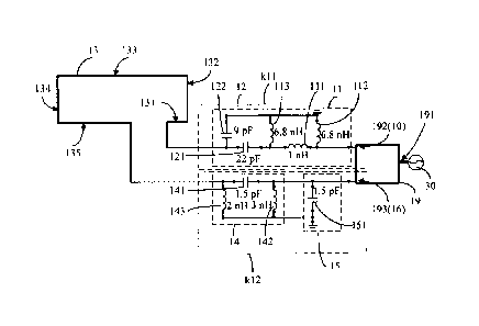
resonance frequency of the 0.5X resonance mode generated by matching.
100911 FIG. 1-11 is a schematic diagram of basic current distribution of
the
antenna apparatus in the 1.5A. resonance mode. The second filter circuit 14
and the
second matching circuit 15 are omitted in the figure. The 1.5X resonance mode
is
similar to the 1X resonance mode shown in FIG. 1-10. However, a difference is
that
the second feedpoint 16 feeds the electromagnetic wave signal whose wavelength
is A,
a wavelength corresponding to the electromagnetic wave during resonance is 1.5
A,
three current reversal points are generated when the radiator 13 is excited,
and the
three current reversal points are approximately located at midpoints of the
first
segment 131, the third segment 113, and the fifth segment 135 of the radiator
13. With
reference to FIG. 1-7, the frequency MB2 of a resonance frequency of the 1.5X
resonance mode is closer to 2.2 GHz in the horizontal coordinate, and is
greater than
the frequency MB1 of the resonance frequency of the 11 resonance mode.
100921 FIG. 1-12 is a schematic diagram of basic current distribution of
the
antenna apparatus in the 2.0X resonance mode. The second filter circuit 14 and
the
second matching circuit 15 are omitted in the figure. The 2.0X resonance mode
is
similar to the 1A, resonance mode shown in FIG. 1-10. However, a difference is
that
the second feedpoint 16 feeds the electromagnetic wave signal whose wavelength
is A,
a wavelength corresponding to the electromagnetic wave during resonance is 2.0
A,
four current reversal points are generated when the radiator 13 is excited,
the four
current reversal points are approximately located at the first segment 131,
the third
segment 113, and the fifth segment 135 of the radiator 13, and extension
lengths of
the four current reversal points on the radiator 13 are approximately the
same. With
reference to FIG. 1-7, the frequency HB1 of a resonance frequency of the 2.0X
CA 03076260 2020-03-18
resonance mode is closer to 2.7 GHz in the horizontal coordinate, and is
greater than
the frequency MB2 of the resonance frequency of the 1.5k resonance mode.
100931 FIG. 1-13 is a schematic diagram of basic current distribution of
the
antenna apparatus in the 2.5k resonance mode. The second filter circuit 14 and
the
second matching circuit 15 are omitted in the figure. The 2.5X resonance mode
is
similar to the 1A, resonance mode shown in FIG. 1-10. However, a difference is
that
the second feedpoint 16 feeds the electromagnetic wave signal whose wavelength
is?.,
a wavelength corresponding to the electromagnetic wave during resonance is 2.5
k,
five current reversal points are generated when the radiator 13 is excited,
the five
current reversal points are approximately located at the first segment 131,
the second
segment 112, the third segment 113, the fourth segment 114, and the fifth
segment 135
of the radiator 13, and extension lengths of the five current reversal points
on the
radiator 13 are approximately the same. With reference to FIG. 1-7, the
frequency
HB2 of a resonance frequency of the 2.5k resonance mode is closer to 3GHz in
the
horizontal coordinate, and is greater than the frequency HB1 of the resonance
frequency of the 2.0A, resonance mode.
100941 FIG. 1-14 is a partial schematic structural diagram of a terminal
in which
the antenna apparatus in an implementation is disposed. The terminal includes
a
mother board 01 and a mainboard 02. The mainboard 02 is disposed above the
mother
board 01 in a stack manner, and a USB interface 021 is disposed on a side of
the
mainboard 02. The first feeding branch circuit k 1 1 and the second feeding
branch
circuit k 1 2 of the antenna apparatus are disposed on the mainboard 021. In
addition,
the first feeding branch circuit k 1 1 is disposed on a left side of the USB
interface 021,
and the second feeding branch circuit k12 is disposed on a right side of the
USB
interface 021. The radiator 13 of the antenna apparatus is disposed on a side
of the
USB interface 021. Specifically, the first segment 131 is parallel to a plane
on which
the mainboard 02 is located and is disposed on the left side of the USB
interface 021,
and there is a distance between the first segment 131 and the plane on which
the
mainboard is located. The second segment 132 is approximately perpendicular to
an
extension direction of the first segment 131, and is approximately parallel to
the plane
21
CA 03076260 2020-03-18
on which the mainboard 02 is located. The third segment 133 is approximately
perpendicular to an extension direction of the second segment 132, the second
segment 132 is connected to one end of the third segment 133, and the third
segment
133 is approximately perpendicular to the plane on which the mainboard 02 is
located.
The fourth segment 134 is approximately perpendicular to an extension
direction of
the third segment 133, and is approximately parallel to the plane on which the
mainboard 02 is located, and the fourth segment 134 is connected to the other
end
opposite to the third segment 133. The fifth segment 135 is approximately
perpendicular to an extension direction of the fourth segment 134, and is
.. approximately parallel to the plane on which the mainboard 02 is located,
the fifth
segment 135 is located at the right side of the USB interface 021, and the
fifth
segment 135 and the first segment 131 are approximately located on a same
plane.
According to the disposing, the antenna apparatus is symmetrically disposed
relative
to the USB interface 021, so that a structure is simple.
100951 Referring to FIG. 1-14 and FIG. 1-15, FIG. 1-15 is a schematic plane
diagram of FIG. 1-14. A first contact 1313 is electrically connected to the
first feeding
branch circuit kll, and a second contact 1353 is electrically connected to the
second
feeding branch circuit k12. The first segment 131 of the radiator 13 is
electrically
connected to the first contact 1313, and the fifth segment 135 is electrically
connected
to the second contact 1353. Specifically, the first segment 131 may be
electrically
connected to the first contact 1313 by using a first spring plate 1312, and
the fifth
segment 135 may be electrically connected to the second contact 1353 by using
a
second spring plate 1352. Because the first segment 131 and the fifth segment
135 of
the radiator 13 are higher than the plane on which the mainboard 02 is
located, the
first spring plate 1312 and the second spring plate 1312 may be disposed to be
perpendicular to the plane on which the mainboard 02 is located. In this way,
there is
a sufficient distance between the radiator 13 and each of the first feeding
branch
circuit k 1 1 and the second feeding branch circuit k12, so that radiation
generated by
current flows of the first feeding branch circuit k 11 and the second feeding
branch
circuit k 1 2 on the mainboard 02 does not interfere with a radiation
characteristic of
22
CA 03076260 2020-03-18
the radiator 13.
[0096] Because the USB interface 021 on the terminal needs to reserve
space
facing outside of the terminal, a first through-hole 1331 is disposed at a
location that
is of the third segment 133 of the radiator 13 and that is corresponding to
the USB
interface 021. In addition, because a headset, a microphone interface, or
another
interface needs to be disposed, a second through-hole 1332 is disposed on the
third
segment 133. To prevent a difference between the radiation characteristic of
the
radiator 13 and a radiation characteristic of a radiator 13 with a uniform
structure
from being very large, a first block 1311 is disposed on the first segment
131, and a
second block 1351 is disposed on the fifth segment 135. The first block 1311
is
equivalent to a protruded block that is of the first segment 131 and that is
parallel to
the plane on which the mainboard 02 is located, and the second block 1351 is
equivalent to a protruded block that is of the fifth segment 135 and that is
parallel to
the plane on which the mainboard 02 is located. In addition, a protruded block
1314 is
electrically connected to the first block 1311, and the protruded block 1314
is located
on the same plane on which the mainboard 02 is located. A radiation
characteristic of
the antenna apparatus may be adjusted by disposing the first block 1311, the
second
square 1353, and the protruded block 1314.
[0097] FIG. 1-16 a partial schematic diagram of a terminal in which the
antenna
apparatus in another implementation is disposed. FIG. 1-17 is a schematic
plane
diagram of FIG. 1-16. A structure of the antenna apparatus disposed in the
terminal in
this implementation is basically the same as that in the previous
implementation. A
difference is that the first feeding branch circuit k 11 and the second
feeding branch
circuit k12 are disposed on a same side of the USB interface 021. Because the
terminal includes many components, to reserve space for arranging another
component, the first feeding branch circuit kll and the second feeding branch
circuit
k12 are disposed on the same side of the USB interface 021. In this way, the
structure
is more flexible.
[0098] Similar to the antenna apparatus in the previous implementation, a
block (a
number 1351 in FIG. 4-2 and FIG. 4-3 is used as an example) for tuning is also
23
CA 03076260 2020-03-18
disposed on the radiator 13 in this implementation, and the first through-hole
1331 is
also disposed on the third segment 133 for exposing the USB interface 021. In
addition, the second through-hole 1332 may be disposed based on a specific
structure
of the terminal for exposing another component such as a microphone interface.
[0099] In this embodiment, the third segment 133 of the radiator 13 may be
configured as a metal frame of the terminal. Further, the metal frame may be
configured as a frame on a side of the USB interface. In this case, there is
no other
metal shielding, so that the antenna apparatus does not need to consider
clearance. In
another embodiment, the third segment 133 of the radiator 13 may be
alternatively
configured inside the terminal. In this case, a clearance area needs to be
left on the
terminal, to avoid metal shielding. For example, a manner in which a housing
of the
terminal is configured as a non-metal material, a manner in which a metal
housing of
the terminal is slit, or the like may be used.
[0100] FIG. 1-18 is a schematic diagram of Sll (input return loss) of the
antenna
apparatus in an implementation. There are six low points on input return loss
curves in
the figure of S11, and the six low points are respectively corresponding to
resonance
frequencies of six resonance. This indicates that in this embodiment of this
application,
bandwidth of the antenna apparatus is wide enough, and the radiation
characteristic
meets a multi-frequency requirement.
[0101] FIG. 2-1 is a schematic structural diagram of an antenna apparatus
according to a second embodiment of this application. Referring to FIG. 2-1,
the
antenna apparatus is basically the same as an antenna apparatus in the first
embodiment. However, a difference is that the antenna apparatus further
includes a
first switch 17 and at least one ground branch 171. The at least one ground
branch 171
is connected in parallel between the first switch 17 and a ground. The first
switch 17
is electrically connected to the radiator 13 and is disposed on a side of the
radiator that
is close to the second feeding branch circuit k12. The first switch 17
cooperates with
the at least one ground branch 171 to switch an electrical length of a signal
of the first
frequency band. In an implementation, there is one ground branch 171. In
another
implementation, there are at least two ground branches 171.
24
CA 03076260 2020-03-18
[0102] Specifically, one end of the first switch 17 is electrically
connected to a
fifth segment 135 of the radiator 13, and the other end is grounded. Further,
an
impedance component 172 is connected in series between the at least one ground
branch 171 and the ground. The impedance component 172 may include a resistor,
an
inductor, or a capacitor. For example, when the first switch 17 is in a turn-
off status,
the antenna apparatus in this embodiment is the same as the antenna apparatus
in the
first embodiment. When the first switch 17 is connected to an impedance
component
172 to which an inductor is connected in series, because the inductor has a
characteristic of allowing a low frequency signal to pass through and
hindering a high
frequency signal, a low frequency signal that is of the first frequency band
and that is
fed by a first feedpoint 10 is directly grounded at the first switch 17, so
that a physical
electrical length of the radiator 13 of the antenna apparatus is shortened, to
be specific,
a part that is of the radiator 13 and that is configured to radiate a signal
lacks a
segment that is on the fifth segment 135 and that is from a point electrically
connected
to the first switch 17 to the second feeding branch circuit k12. In this case,
a
frequency at which the signal of the first frequency band generates resonance
moves
toward a high frequency. When the first switch 17 is connected to a 0-ohm
impedance
component 172, relative to that the first frequency band is directly grounded
at the
first switch 17, the physical electrical length of the radiator 13 is the
shortest, and the
frequency at which the first frequency band generates the resonance is the
highest.
Bandwidth of the first frequency band may be extended by disposing the first
switch
17, the ground branch 171, and the impedance component 172.
[0103] FIG. 2-2 is a schematic diagram of Sll (input return loss) of the
antenna
apparatus in this embodiment. When the first switch 17 is connected to
different
impedance components, it can be seen that a low resonance frequency changes
obviously. In this way, the antenna apparatus in this embodiment can implement
multi-frequency performance, and can adjust the low resonance frequency.
[0104] FIG. 3-1 is a schematic structural diagram of an antenna apparatus
according to a third embodiment of this application. The antenna apparatus is
basically the same as an antenna apparatus in the first embodiment. However, a
CA 03076260 2020-03-18
difference is that the antenna apparatus further includes a radiation branch
20, a
second switch 18, a first ground branch 181, and at least one second ground
branch
182. The first ground branch 181 is connected in series between the second
switch 18
and the second feeding branch circuit k12. The at least one second ground
branch 182
is connected in parallel between the second switch 18 and a ground. The
radiation
branch 18 is electrically connected to an end that is of the second feeding
branch
circuit k12 and that is connected to the first ground branch 181. There may be
one
second ground branch 181, or there may be at least two second ground branches
181.
101051 Specifically, one end of the second switch 18 is electrically
connected to a
fifth segment 135 of a radiator 13. Impedance components 183 may be
electrically
connected to the first ground branch 181 and the at least one second ground
branch
182 respectively. The impedance component 183 may include a resistor, an
inductor,
or a capacitor. The first ground branch 181 is electrically connected to a
second filter
circuit 14 of the second feeding branch circuit k 1 2 by using one impedance
component 183. The at least one second ground branch 182 is electrically
connected
to the ground by using another impedance component 183. A function of the
impedance component 183 is to adjust a physical electrical length of the
radiator 13.
101061 An operating principle of the antenna apparatus in this embodiment
is as
follows: When the second switch 18 is connected to the first ground branch
181, a
signal that is of a first frequency band and that is fed by a first feeding
branch circuit
k 11 is radiated on the radiator 13, and then is grounded at the second filter
circuit 14;
and a signal that is of a second frequency band and that is fed by the second
feeding
branch circuit k12 is radiated on the radiator 13 and the radiation branch 20,
and then,
some of signals on the radiator 13 are grounded at a first filter circuit 12.
In this case,
compared with the first embodiment, a radiation characteristic of the signal
of the
second frequency band changes. When the second switch 18 is connected to and
is
grounded at the second ground branch 182, it is equivalent to that a circuit
between
the radiator 13 and the second feeding branch circuit k12 is broken, and the
signal that
is of the first frequency band and that is fed by the first feeding branch
circuit k 1 1 is
radiated on the radiator 13, and then is grounded at the second switch 18 by
using the
26
CA 03076260 2020-03-18
second ground branch; and the signal that is of the second frequency band and
that is
fed by the second feeding branch circuit k12 is radiated on the radiation
branch 20.
[0107] According to the foregoing disposing, the second switch 18
cooperates
with the first ground branch 181 or the at least one second ground branch 182,
so that
a plurality of operating modes of the antenna apparatus can be implemented. In
this
way, the antenna apparatus has multi-frequency performance, and resonance
frequencies of a high frequency signal and a low frequency signal can be
adjusted.
[0108] In an implementation, the radiation branch 20 is disposed to be
separated
from the radiator 13, and a physical electrical length of the radiation branch
20 is less
than the physical electrical length of the radiator 13. Specifically, a
frequency of the
first frequency band is lower than a frequency of the second frequency band.
The
radiation branch 20 is configured to radiate a signal of a resonance frequency
in the
second frequency band, and a higher frequency indicates a shorter wavelength,
and
requires a shorter physical antenna length. The radiator 13 is configured to
radiate not
only the signal whose resonance frequency is in the second frequency band but
also
a signal whose resonance frequency is in the first frequency band. Therefore,
the
physical electrical length of the radiation branch 20 is disposed to be less
than the
physical electrical length of the radiator 13, so that a requirement of
radiating the
signal of the second frequency band can be met. To avoid mutual radiation
interference, the radiation branch 20 needs to be separated from the radiator
13 by a
specific distance, to ensure sufficient antenna isolation.
[0109] FIG. 4-1 is a schematic diagram of a circuit structure of an
antenna
apparatus according to a fourth embodiment of this application. The first
feeding
branch circuit k 1 1 includes a first capacitor 114, a second capacitor 116, a
third
capacitor 126, a first inductor 115, a second inductor 117, a third inductor
124, and a
fourth inductor 125. The second capacitor 116 is connected in series between
the
second feedpoint 10 and a ground. The second inductor 117 is connected in
series
between the ground and an end that is of the second capacitor 116 and that is
far away
from the ground. The first capacitor 114, the first inductor 115, and the
third inductor
124 are successively connected in series between the ground and an end that is
of the
27
CA 03076260 2020-03-18
second inductor 117 and that is far away from the ground. The fourth inductor
125
and the third inductor 126 are successively connected in series between the
ground
and an end that is of the third capacitor 124 and that is far away from the
ground. The
radiator 13 is electrically connected to an end that is of the fourth inductor
125 and
that is far away from the ground. The first capacitor 114, the second
capacitor 116, the
first inductor 115 and the second inductor 117 form the first matching circuit
11, and
the third capacitor 126, the third inductor 124, and the fourth inductor 125
form the
first filter circuit 12.
[0110] Further, the second feeding branch circuit k12 includes a fourth
capacitor
152, a fifth capacitor 145, a fifth inductor 153, a sixth inductor 144, and a
seventh
inductor 146. The fifth inductor 153 is connected in series between the second
feedpoint 16 and the ground. The fourth capacitor 152, the fifth capacitor
145, and the
seventh inductor 146 are successively connected in series between the ground
and an
end that is of the fifth inductor 153 and that is far away from the ground.
The sixth
inductor 144 is connected in parallel to two ends of the fifth capacitor 145.
The
radiator 13 is electrically connected to an end that is of the seventh
inductor 146 and
that is far away from the ground. The fourth capacitor 152 and the fifth
inductor 153
form the second matching circuit 15, and the fifth capacitor 145, the sixth
inductor
144, and the seventh inductor 146 form the second filter circuit 14.
[0111] A circuit principle in FIG. 4-1 is as follows: Because an
alternating current
signal has a magnitude-phase characteristic, and a capacitor and an inductor
have
different frequency response characteristics at different frequencies, a
frequency of a
current signal that is of a first frequency band and that is fed by the first
feedpoint 10
is lower than a frequency of a current signal that is of a second frequency
band and
that is fed by the second feedpoint 16. The first capacitor 113 and the first
inductor
114 may allow the signal that is of the first frequency band and whose
frequency is
lower to pass through, and after resonance is generated on the radiator 13,
the current
signal is grounded at the seventh inductor 146 because the sixth inductor 144
and the
fifth capacitor 145 that are connected in parallel hinder a low frequency
signal and an
intermediate frequency signal. The second feedpoint 16 feeds the current
signal of the
28
CA 03076260 2020-03-18
second frequency band. The fourth capacitor 152 may allow the signal that is
of the
second frequency band and whose frequency is higher to pass through. At the
sixth
inductor 144 and the fifth capacitor 145 that are connected in parallel, a
high
frequency part of the current signal passes through the sixth inductor 144,
and a super
high frequency part passes through the fifth capacitor 145. After resonance is
generated on the radiator 13, the current signal is grounded at the first
filter circuit 12
or the first matching circuit 11. To adjust impedance matching of the antenna,
bypass
capacitors and bypass inductors of the second capacitor 116, the second
inductor 117,
the third inductor 124, the fourth inductor 125, the third capacitor 126, the
fifth
inductor 153, and the seventh inductor 146 that are grounded need to be
disposed, so
as to adjust impedance matching of the antenna apparatus to an ideal status.
[0112] The sixth inductor 144 and the fifth capacitor 145 that are
connected in
parallel are equivalent to a band-stop filter component added to the second
filter 14,
so that a resonance frequency of the antenna apparatus includes a low
frequency part
and an intermediate frequency part. This is equivalent to that a low frequency
signal
of a first frequency band and an intermediate frequency signal of a second
frequency
band of an antenna apparatus in the first embodiment cannot pass through, and
in the
second frequency band, a high frequency part is further separated from a super
high
frequency part. Therefore, antenna bandwidth is extended.
[0113] Specific values of each capacitor and each inductor in FIG. 4-1 are
not
limited in this application. However, for better understanding, a preferred
implementation is provided. As marked in FIG. 4-1, a capacitance value of the
first
capacitor 114 is 2.2 pF, an inductance value of the first inductor 115 is 6.8
nH, a
capacitance value of the second capacitor 116 is 2.5 pF, an inductance value
of the
second inductor 117 is 5.3 nH, an inductance value of the third inductor 124
is 5 nH,
an inductance value of the fourth inductor 125 is 6 nH, a capacitance value of
the third
capacitor 126 is 0.65 pF, a capacitance value of the fourth capacitor 152 is
1.8 pF, an
inductance value of the fifth inductor 153 is 0.8 nH, an inductance value of
the sixth
inductor 144 is 2.5 nH, a capacitance value of the fifth capacitor 145 is 3.3
pF, and an
inductance value of the seventh inductor 146 is 2.7 nH.
29
CA 03076260 2020-03-18
[0114] FIG. 4-2 is a schematic diagram of Sll (input return loss) of the
antenna
apparatus shown in FIG. 4-1. It can be seen that the antenna apparatus
includes two
low resonance frequencies, two intermediate resonance frequencies, one high
resonance frequency, and one super high resonance frequency. In this way,
performance of the antenna apparatus meets a multi-frequency requirement.
[0115] FIG. 5-1 is a schematic diagram of a circuit structure of an
antenna
apparatus according to a fifth embodiment of this application. The antenna
apparatus
is basically the same as an antenna apparatus in the first embodiment.
However, a
difference is that a duplexer 19 is disposed. The duplexer 19 includes an
input port
191, a first output port 192, and a second output port 193. The first output
port 192 is
configured as the first feedpoint 10, and the second output port 193 is
configured as
the second feedpoint 16. The first filter circuit 12 is electrically connected
to the first
output port 192, the second filter circuit 14 is electrically connected to the
second
output port 193. The antenna apparatus further includes a general feedpoint
30. The
general feedpoint 30 is electrically connected to the input port 191.
[0116] Specifically, a function of the duplexer 19 is to classify
signals fed by the
general feedpoint 30 into two paths of signals that are isolated from each
other, to be
specific, a signal that is of a first frequency band and that is output by the
first output
port 192 and a signal that is of a second frequency band and that is output by
the
second output port 192. In other words, the duplexer 19 is disposed, so that
functions
of a first feedpoint 10 and a second feedpoint 16 in the first embodiment can
be
implemented by disposing only the general feedpoint 30. In this way, a
quantity of
feedpoints is reduced. This facilitates a space layout of components inside a
terminal.
[0117] It may be learned from the foregoing description that in this
embodiment, a
first feeding branch circuit kl 1 includes the first output port 192, a first
matching
circuit 11, and the first filter circuit 12, and a second feeding branch
circuit k12
includes the second output port 193, a second matching circuit 15, and the
second
filter circuit 14.
101181 The circuit structure in this embodiment is the same as a circuit
structure in
the first embodiment, and details are not described herein again.
CA 03076260 2020-03-18
[0119] An implementation of electrically connecting the first feeding
branch
circuit kll and the second feeding branch circuit k12 to a radiator 13 is
basically the
same as an implementation of electrically connecting a first feeding branch
circuit kl 1
and a second feeding branch circuit k12 to the first area B1 in the first
embodiment. In
this embodiment, a length of a first segment 441 is short, and a length of a
fifth
segment 445 is long, so that an offset feeding structure forms on the radiator
44.
According to the disposing, the first feeding branch circuit kl 1 and the
second feeding
branch circuit k12 may be away from a location at which another component is
arranged on the terminal. This facilitates a layout of the components of the
terminal.
[0120] Certainly, the first feeding branch circuit kl 1 and the second
feeding
branch circuit k12 may be electrically connected to the radiator 13 in this
embodiment
by alternatively using an implementation of electrically connecting the first
feeding
branch circuit kl 1 and the second feeding branch circuit k12 to the second
area B2.
[0121] FIG. 5-2 is a schematic diagram of S1 1 (input return loss) of an
antenna
apparatus shown in FIG. 5-1. It may be seen that there are two low resonance
frequencies and four intermediate and high resonance frequencies. In this way,
multi-frequency performance of the antenna apparatus is achieved.
[0122] The antenna apparatus and the terminal provided in the embodiments
of
this application are described in detail above. The principle and
implementation of
.. this application are described herein through specific examples. The
description about
the embodiments of this application is merely provided to help understand the
method
and core ideas of this application. In addition, a person of ordinary skill in
the art can
make variations and modifications to this application in terms of the specific
implementations and application scopes according to the ideas of this
application.
.. Therefore, the content of specification shall not be construed as a limit
to this
application.
31