Note: Descriptions are shown in the official language in which they were submitted.
CA 03076933 2020-03-25
WO 2019/060990
PCT/CA2018/051203
TITLE: POLYMER FILM-METAL COMPOSITES
CROSS-REFERENCE TO RELATED APPLICATIONS
[0001] The present application claims the benefit of priority from co-
pending U.S. provisional application no. 62/563,170 filed on September 26,
2017, the contents of which are incorporated herein by reference in their
entirety.
FIELD
[0002] The present application relates to polymer film-metal
composites,
to methods of preparing polymer film-metal composites and to uses of such
composites. The metal can be in the form of a nanoparticle or a film.
BACKGROUND
[0003] Metallic nanoparticles exhibit advantageous geometry and size-
related properties that differ significantly from those observed in the
corresponding bulk materials. Their incorporation in polymer matrices
including
thermoplastics (such as but not limited to polystyrene, polycarbonate,
poly(methyl methacrylate) (PMMA) and polydimethylsiloxane (PDMS))
thermosets (such as but not limited to epoxy resins, polyimides and
polyesters)
or UV curable resists or materials may, for example, lead to nanocomposites
with desirable electrical, optical, chemical, magnetic, dielectric and/or
mechanical properties, compared to their microparticle-reinforced
counterparts.
While not wishing to be limited by theory, this is mostly due to high surface-
area
to volume ratios of homogeneous nanoparticle dispersions in the polymer
matrix. However, achieving a homogeneous and uniform dispersion of
nanoparticles or having nanoparticles of a particular geometry dispersed
within
the pre-polymer matrix can be challenging.
[0004] Several methods have been used to fabricate metal-polymer
nanocomposites, including the vapor phase deposition of metallic particles
onto
polymer matrices and reducing metal ions in polymer gels and homogenizing
polymer and nanosized metal powders [1,2]. Typically, this entails multistep
methods as the polymerization of organic monomer and the formation of
nanosized metal particles are performed separately, so that the metal
particles in
the polymer matrix are not homo-dispersed [1]. For instance, metallic
nanoparticles
- 1 -
CA 03076933 2020-03-25
WO 2019/060990
PCT/CA2018/051203
of particular size and shape can be synthetized first using well-known batch
chemical methods. These particles can then be dispersed into a polymerizable
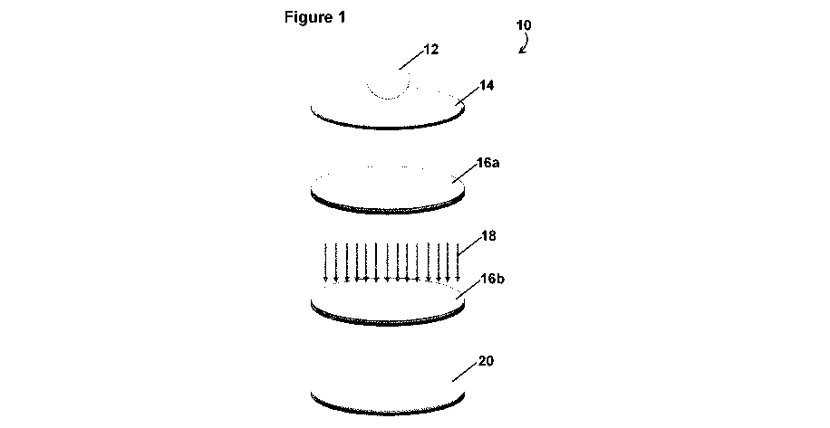
formulation using physical methods including ultrasonic agitation, shear
mixing or
ball milling [3]. The mixed pre-polymer matrix is finally polymerized in order
to
obtain the final polymer film with embedded nanoparticles.
[0005]
Following the polymerization reaction using such techniques, the
nanoparticle distribution within the resulting polymer films would be random.
In other words, for the fabrication of nanocomposite materials, spatial
positioning of the nanoparticles, including but not limited to distribution
across
the matrix and/or a thin layer of nanoparticles or a continuous metallic film
due
to percolation of nanoparticles may not be achieved using such techniques.
[0006]
Composites containing noble metal particles are interesting, for
example, due to their advantageous optical properties which arise from their
ability to support surface plasmons whose frequency depends on the material,
size, shape, and/or the surrounding environment of the nanoparticle. Of these,
polymer films containing gold nanoparticles may be of particular interest due
to
potential applications in flexible sensors and energy storage [3]. For these
applications, precise control of particle size, shape and/or dispersion within
the
polymer matrix may be desirable, for example, as small changes of the
configuration of the composite such as the total metal content as well as the
size
and/or the shape of the nanoparticles can lead to dramatic changes in the
electrical and optical properties of the material [4]. However, gold
nanoparticles
possess high surface free energy and are thus prone to agglomeration.
[0007] As noted
above, control of nanoparticle dispersion within the
polymer matrix using traditional ex-situ or in-situ physical methods for pre-
polymer matrix preparation is complex and challenging, limiting its interest
for
practical applications. In addition, volume mixing of pre-synthesized
particles with
a polymer matrix has not led to spatially localized (in 2D or 3D)
distributions of
nanoparticles nor continuous metallic layers inside a polymer matrix.
[0008] An in-
situ simultaneous polymerization-reduction approach to
synthesis of polymer-metal nanocomposites has been reported wherein the
- 2 -
CA 03076933 2020-03-25
WO 2019/060990
PCT/CA2018/051203
polymerization of the organic monomer is carried out in parallel with the
formation of the metal nanoparticles [5]. For example, the review article by
RangaReddy et al. discloses that metal particles can be generated inside a
polymer matrix by decomposition (e.g., thermolysis, photolysis, radiolysis,
etc.)
or chemical reduction of a metallic precursor dissolved into the polymer [5].
Yagci et al. have shown UV induced radical polymerization of an acrylic resin
(poly(ethylene glycol diacrylate, PEGDA) and an epoxy resin (1,3-bis(3,4-
epoxycyclohexylethyl)tetramethyldisiloxane, EPDX) and gold nanoparticle
formation by the reduction of gold (Ill) chloride hydrate (HAuC14) in the
presence of a photoinitiator (lrgacureTM 2959 or camphorquinone, respectively)
[6,7].Yagci et al. stated that nanoparticle size depended on the concentration
of
the gold precursor in the pre-polymer mix, however due to particle
agglomeration even at very low precursor concentrations (1%, 3% and 5% wt),
the process suffered from poor control of the gold nanoparticles distribution
in
the polymer matrix in addition to having polydisperse particle size [6]. The
distribution and orientation of the larger gold nanoparticles was also random.
SUMMARY
[0009] The
methods of the present application were used to prepare
both plasmonic and conductive metal structures in situ in polymer materials.
Polymer-metal composite films were obtained using a wide concentration
range of nanoparticle loading, well controlled nanoparticle distribution in
the
polymer matrix and long-term thermodynamic stability. Examples were
observed wherein the geometry and/or the orientation of large metallic
particle
growth was controlled as a result of smaller particle migration through the
polymer network by structuration of the polymer films. The methods can be
used to fabricate embedded metallic films in the form of metallic traces,
metallic
shells, or metallic stacks embedded on the coating and inside a hollow cavity,
for example on the top, bottom, or the side-walls of fluidic channels,
chambers
or reservoirs. The formation of the polymer-metal composite films can be
obtained on various solid surfaces, independent of the components, shapes
and/or microstructures of the substrates.
- 3 -
CA 03076933 2020-03-25
WO 2019/060990
PCT/CA2018/051203
[0010]
Accordingly, the present application includes a method for
preparing a polymer film-metal composite, the method comprising:
depositing on a surface, a composition comprising:
a cationic metal precursor;
a polymer film precursor that comprises a plurality of
photopolymerizable groups; and
a photoreducer-photoinitiator, and
irradiating the composition under conditions to simultaneously reduce
the cationic metal and polymerize the photopolymerizable groups to
obtain the polymer film-metal composite on the surface.
[0011] The
present application also includes a polymer film-metal
nanoparticle composite comprising a uniform distribution of metal
nanoparticles embedded in a polymeric resin film, the polymeric resin
comprising a plurality of metal-anchoring groups, the metal anchoring groups
anchored to the nanoparticles, a polymer film-metal nanoparticle composite
comprising an ordered distribution of metal nanoparticles embedded in a
polymeric resin film; and a polymer film-metal film composite comprising a
continuous film of the metal embedded in a polymeric resin film.
[0012] The
present application also includes uses of the polymer film-
metal nanoparticle and film composites of the application.
[0013] Other
features and advantages of the present application will
become apparent from the following detailed description. It should be
understood,
however, that the detailed description and the specific examples while
indicating
embodiments of the application are given by way of illustration only, since
various
changes and modifications within the spirit and scope of the application will
become apparent to those skilled in the art from this detailed description.
BRIEF DESCRIPTION OF THE DRAWINGS
[0014] The
present application will now be described in greater detail
with reference to the drawings in which:
- 4 -
CA 03076933 2020-03-25
WO 2019/060990
PCT/CA2018/051203
[0015] Figure 1
is a schematic of an embodiment of a method for
preparing a polymer film-metal composite of the present application
comprising flood exposure of a precursor composition thereto on a surface.
[0016] Figure 2
is a schematic of an embodiment of a method for
preparing a polymer film-metal composite of the present application comprising
flood exposure of a precursor composition thereto on a surface through a
topographically structured template comprising micro- or nanostructures that
are replicated as a negative on a surface of the composite film.
[0017] Figure 3
is a schematic of an embodiment of a method for
preparing a polymer film-metal composite of the present application
comprising photolithography, with the precursor composition to the composite
being irradiated through a mask defining a desired pattern.
[0018] Figure 4
is a schematic of an embodiment of a method for
preparing a polymer film-metal composite of the present application
comprising a large-scale fabrication technique such as roll-to-roll
processing.
[0019] Figure 5
is a photograph of poly(ethylene glycol)-diacrylate PEGDA
polymer film-silver nanoparticle composites according to embodiments of the
present application prepared with exposure times of from 5 seconds to 1
minute.
[0020] Figure 6
shows a photograph (left) and scanning electron
microscopy (SEM) images (middle and right) at increasing magnification (as
indicated by boxes) of conductive continuous gold films fabricated using flood
exposure of the precursor composition comprising PEGDA (MW = 700 Da) at
10% cationic metal precursor concentration according to an embodiment of a
method for preparing a polymer film-metal composite of the present
application. Scale bars show 50.0 p.m (middle) and 1.00 pm (right).
[0021] Figure 7
shows scanning electron microscopy (SEM) images at
increasing magnification (as indicated by boxes) of conductive continuous
silver films fabricated using flood exposure of the precursor composition
comprising PEGDA (MW = 700 Da) at 10% cationic metal precursor
concentration according to an embodiment of a method for preparing a
- 5 -
CA 03076933 2020-03-25
WO 2019/060990
PCT/CA2018/051203
polymer film-metal composite of the present application. Scale bars show 20
p.m (left), 30.0 pm (middle) and 1.00 pm (right).
[0022] Figure 8
shows photographs of polymer film (PEGDA, MW =
700 Da)-gold nanoparticle composites prepared with varying concentrations of
cationic gold metal precursor and thus different nanoparticle sizes according
to embodiments of the method for preparing a polymer film-metal composite
of the present application. In color photographs, different colors of polymer
film-gold nanoparticle composites are observed that depend on the gold
particle size as a plasmonic signature.
[0023] Figure 9
is a plot comparing the absorbance measurements of
composites of the present application prepared from PEGDA versus ethoxylated
trimethylolpropane triacrylate (ETPTA) prepared according to an embodiment of
a method for preparing a polymer film-metal composite of the present
application
comprising flood exposure of the precursor composition at 10% cationic metal
precursor concentration under conditions to form gold nanoparticles.
[0024] Figure
10 shows Raman measurements of native polymer films
compared to polymer film-gold nanoparticle composites prepared using PEGDA
and ETPTA monomers according to methods of the present application, showing
distinct peaks at low wavenumbers due to gold nanoparticles.
[0025] Figure
11 shows an SEM image of a polymer film-metal
nanoparticle composite prepared according to an embodiment of a method for
preparing a polymer film-metal composite of the present application
comprising imprint lithography (left) and SEM images at successive
magnifications (middle and right images) of features in the image at the left,
as indicated by boxes. Scale bars show 2.00 mm (left); 5.00 p.m (top middle),
1.00 pm (top right), 30.0 pm (bottom middle) and 3.00 p.m (bottom right).
[0026] Figure
12 shows SEM images comparing polymer film-metal
composites according to embodiments of the methods of present disclosure
using an imprint lithography method with a flat mold (top) and a
nanostructured mold containing 700 nm line gratings (bottom). The
nanostructures guided the metallic nanoparticles' nucleation and
- 6 -
CA 03076933 2020-03-25
WO 2019/060990
PCT/CA2018/051203
agglomeration which occurred along the grating lines. Nanoparticles
agglomerated in regular polygonal geometrical shapes (bottom images), as
opposed to random nanoparticle distribution and shape on a flat substrate
(top images). Scale bars show 10.0 pm (top images; both main and inset),
200 p.m (bottom main image) and 20.0 pm (top left inset of bottom images).
[0027] Figure
13 shows SEM images of guided nucleation, growth and
agglomeration of metallic nanoparticles into regular geometrical shapes with
apexes aligned with nanostructured grating lines prepared according to
embodiments of a method for preparing a polymer film-metal composite of the
present application using a nanostructured template. Scale bars on top row
show 10.0 pm (left), 20.0 pm (middle) and 2.0 pm (right). Scale bars on bottom
row show 5.0 pm (left), 4.0 pm (middle) and 4.0 pm (right).
[0028] Figure
14 shows SEM images of a uniform distribution of gold
nanoparticles along the grating lines prepared according to embodiments of a
method for preparing a polymer film-metal composite of the present
application which use a precursor composite containing dithiothreitol (DTT)
with nanoparticle size depending on the cationic metal precursor
concentration 1% wt (top image), 5% wt (middle image) and 10% wt (bottom
image) following irradiation.
[0029] Figure
15 shows SEM images of the fabrication of conductive
traces within a microfluidics device according to an embodiment of the methods
of the present disclosure by co-flowing the precursor composition and an
immiscible liquid and irradiating: empty channel (top left); channel
containing
polymer-metal composite (*) (top right); and successive magnifications of the
composite film showing conductive trace (electrode (**), bottom images). Scale
bars show: 100 pm (top right), 10.0 pm (bottom left) and 1.00 pm (bottom
right).
[0030] Figure
16 is a schematic showing an example of light irradiation
of an exemplary array of pillars causing localized heating.
[0031] Figure
17 shows an example of a microfluidic plasmonic
microheater device (left) with SEM images at successive magnifications
- 7 -
CA 03076933 2020-03-25
WO 2019/060990
PCT/CA2018/051203
(middle and right images) of features in the image at the left, as indicated
by
boxes. Scale bars show 2.00 mm (middle) and 30.0 pm (right).
[0032] Figure 18 is a schematic showing an example of a 3D comb
electrodes system wherein reduction (R) and oxidation (0) are occurring.
[0033] Figure 19 is a schematic showing an example of the preparation
of a molecularly imprinted polymer (MIP) electrochemical sensor film.
[0034] Figure 20 is a schematic showing an example of a method for
preparing a polymer film-metal composite of the present application wherein
the surface is a microchannel of a microfluidics device and a mask is applied
during irradiation of the composition to selectively pattern an electrode.
[0035] Figure 21 is a schematic showing an example of an electrode
configuration that may be used for flow detection in a microfluidics device.
DETAILED DESCRIPTION
I. Definitions
[0036] Unless otherwise indicated, the definitions and embodiments
described in this and other sections are intended to be applicable to all
embodiments and aspects of the present application herein described for
which they are suitable as would be understood by a person skilled in the art.
[0037] In understanding the scope of the present application, the
term
"comprising" and its derivatives, as used herein, are intended to be open
ended terms that specify the presence of the stated features, elements,
components, groups, integers, and/or steps, but do not exclude the presence
of other unstated features, elements, components, groups, integers and/or
steps. The foregoing also applies to words having similar meanings such as
the terms, "including", "having" and their derivatives. The term "consisting"
and its derivatives, as used herein, are intended to be closed terms that
specify the presence of the stated features, elements, components, groups,
integers, and/or steps, but exclude the presence of other unstated features,
elements, components, groups, integers and/or steps. The term "consisting
essentially of", as used herein, is intended to specify the presence of the
- 8 -
CA 03076933 2020-03-25
WO 2019/060990
PCT/CA2018/051203
stated features, elements, components, groups, integers, and/or steps as well
as those that do not materially affect the basic and novel characteristic(s)
of
features, elements, components, groups, integers, and/or steps.
[0038] Terms of
degree such as "substantially", "about" and
"approximately" as used herein mean a reasonable amount of deviation of the
modified term such that the end result is not significantly changed. These
terms of degree should be construed as including a deviation of at least 5%
of the modified term if this deviation would not negate the meaning of the
word it modifies.
[0039] The term
"and/or" as used herein means that the listed items are
present, or used, individually or in combination. In effect, this term means
that
"at least one of" or "one or more" of the listed items is used or present.
[0040] As used
in this application, the singular forms "a", "an" and "the"
include plural references unless the content clearly dictates otherwise. For
example, an embodiment including "a polymer film precursor" should be
understood to present certain aspects with one polymer film precursor or two
or more additional polymer film precursors. In embodiments comprising an
"additional" or "second" component, such as an additional or second polymer
film precursor, the second component as used herein is chemically different
from the other components or first component. A "third" component is different
from the other, first, and second components, and further enumerated or
"additional" components are similarly different.
[0041] In
embodiments of the present application, the compounds
described herein have at least one asymmetric center. Where compounds
possess more than one asymmetric center, they may exist as diastereomers.
It is to be further understood that while the stereochemistry of the compounds
may be as shown in any given compound listed herein, such compounds may
also contain certain amounts (e.g. less than 20%, optionally less than 10%,
optionally less than 5%, optionally less than 1%) of compounds having
alternate stereochemistry.
- 9 -
CA 03076933 2020-03-25
WO 2019/060990
PCT/CA2018/051203
[0042] The term
"suitable" as used herein means that the selection of
specific reagents or conditions will depend on the reaction being performed
and the desired results, but none-the-less, can generally be made by a person
skilled in the art once all relevant information is known.
[0043] The term
"dithiothreitol" and the abbreviation "DTT" refer to a
compound having the following structure:
OH
SH
HS7
OH
=
[0044] The term
"poly(ethylene glycol)-diacrylate" and the abbreviation
"PEGDA" as used herein refer to a monomer having the following structure:
- 0
H2C
- n
0
wherein n is dependent on the molecular weight of the PEGDA. For example,
commercial sources of PEGDA include those available from Aldrich having an
average Mn of about 200, 575 and 700.
[0045] The term
"ethoxylated trimethylolpropane triacrylate" and the
abbreviation "ETPTA" as used herein refer to a monomer having the following
structure:
Ra
o
Rb
Rc
wherein Ra, Rb and IRc have the structure:
0
-10-
CA 03076933 2020-03-25
WO 2019/060990
PCT/CA2018/051203
wherein each m may be the same or different and is dependent on the
molecular weight of the ETPTA. For example, commercial sources of ETPTA
include those available from Aldrich having an average Mn of about 428, 692
and 912 as well as those available from Sartomer having a molecular weight
of 428 g/mol (SR-454), 693 g/mol (SR-502) and 956 g/mol (SR-9035).
[0046] The term
"metal-anchoring group" as used herein refers to a
functional group capable of bonding to a surface of a metal e.g. a metal
nanoparticle.
[0047] The term
"cationic metal precursor" as used herein refers to a
compound in which the metal exists in cationic form and is reduced under the
conditions used for photopolymerization in the methods for preparing a
polymer film-metal composite of the present application.
II. Methods
[0048] The
methods of the present application were used to prepare
both plasmonic and conductive metal structures in situ in polymer materials.
Polymer-metal composite films were obtained using a wide concentration
range of nanoparticle loading, well controlled nanoparticle distribution in
the
polymer matrix and long-term thermodynamic stability. Examples were
observed wherein the geometry and/or the orientation of large metallic
particle
growth was controlled as a result of smaller particle migration through the
polymer network by structuration of the polymer films. The methods can be
used to fabricate embedded metallic films in form of metallic traces, metallic
shells, or metallic stacks embedded on the coating and inside a hollow cavity,
for example on the top, bottom, or the side-walls of fluidic channels,
chambers
or reservoirs. The formation of the polymer-metal composite films can be
obtained on various solid surfaces, independent of the components, shapes
and/or microstructures of the substrates.
[0049]
Accordingly, the present application includes a method for
preparing a polymer film-metal composite, the method comprising:
depositing on a surface, a composition comprising:
a cationic metal precursor;
-11 -
CA 03076933 2020-03-25
WO 2019/060990
PCT/CA2018/051203
a polymer film precursor that comprises a plurality of
photopolymerizable groups; and
a photoreducer-photoinitiator, and
irradiating the composition under conditions to simultaneously reduce
the cationic metal and polymerize the photopolymerizable groups to
obtain the polymer film-metal composite on the surface.
[0050] The
surface is any suitable surface. In some embodiments, the
surface comprises a polymer, a glass, a silicon wafer or a paper. In an
embodiment, the polymer is polycarbonate (PC), polystyrene (PS),
poly(methyl methacrylate) (PMMA), polyethylene terephthalate (PET) or a
cyclo-olefin polymer such as ZeonorTM. In some embodiments, the surface is
the inside of a hollow cavity. In another embodiment, the hollow cavity is a
microchannel, a microchamber or a microreservoir. In a further embodiment,
the hollow cavity is a microchannel.
[0051] The
conditions for irradiation can be any suitable conditions. In
some embodiments, the irradiating comprises flood exposure of the
composition deposited on the surface. An exemplary schematic of such an
embodiment 10 of the method for preparing a polymer film-metal composite of
the present application is shown in Figure 1. Referring to Figure 1, in the
exemplified embodiment 10, the composition 12 is deposited on the surface 14
such that a layer 16a of the composition is deposited. Then, the layer 16b of
the
composition is irradiated via flood exposure 18 to simultaneously reduce the
cationic metal and polymerize the photopolymerizable groups to obtain the
polymer film-metal composite 20.
[0052] The
conditions for irradiation may also comprise a suitable
nanoimprint lithography technique. Accordingly, in some embodiments wherein
the irradiating comprises flood exposure of the composition deposited on the
surface, the surface is imprinted with a pattern. An exemplary schematic of
such an embodiment 100 of the method for preparing a polymer film-metal
composite of the present application is shown in Figure 2. Referring to Figure
2,
in the exemplified embodiment 100, the composition 112 is deposited on the
- 12-
CA 03076933 2020-03-25
WO 2019/060990
PCT/CA2018/051203
surface 114 such that a layer 116a of the composition is deposited. Then, the
layer 116b of the composition is imprinted with a pattern via template 117
while
being irradiated via flood exposure 118 to simultaneously reduce the cationic
metal and polymerize the photopolymerizable groups to obtain the polymer film-
metal composite 120. Alternatively, in some embodiments (not shown in Figure
2), the composition is first deposited in a template, then covered by the
surface
(thereby depositing the composition on the surface) and subsequently
irradiated. It will be appreciated by a person skilled in the art that in such
embodiments, the composite has the negative of the surface pattern imprinted
thereon. Accordingly, in some embodiments, the pattern is imprinted on the
surface via a template having a desired pattern. The template can be any
suitable template. For example, it will be appreciated by a person skilled in
the
art that the template is formed of a material that is transparent to the
irradiation
(i.e. it allows the transmission of the irradiation through the template such
that
the irradiation is capable of initiation of the reduction/polymerization of
the
composite precursors). In an embodiment, the template is a polymeric working
stamp. In another embodiment, the template comprises a cyclo-olefin polymer
(e.g. ZeonexTM) or a polydimethylsiloxane. Templates and methods for
preparing such templates having a desired pattern are known and can be
selected by a person skilled in the art. In an embodiment, the template
comprises features that are in the microscale (i.e. from about 1 pm to less
than 1,000 p.m), features that are in the nanoscale (i.e. from about 1 nm to
less than 1,000 nm) or combinations thereof. In an embodiment, the features
are microscale features. In another embodiment, the features are nanoscale
features. In a further embodiment, the features are a combination of
microscale features and nanoscale features. In an embodiment, the features
are circular. In another embodiment, the features are lines. In an embodiment,
the lines are arranged in a grating. In another embodiment, the grating is
from
about 500 nm to about 900 nm or about 700 nm. In some embodiments of the
present application, the method further comprises removing the template from
the composite. In some embodiments, the method further comprises removing
the composite from the surface to obtain a composite that has the negative of
-13-
CA 03076933 2020-03-25
WO 2019/060990
PCT/CA2018/051203
the surface pattern templated thereon. It will be appreciated by a person
skilled in the art that in such embodiments, the material forming the template
and/or the surface is selected such that it allows the release of the
composite.
[0053]
Alternatively, the conditions for irradiation may comprise a
suitable photolithographic technique. Accordingly, in some embodiments, the
irradiating comprises exposure of the composition deposited on the surface
through a mask defining a pattern. An exemplary schematic of such an
embodiment 200 of the method for preparing a polymer film-metal composite
of the present application is shown in Figure 3. Referring to Figure 3, in the
exemplified embodiment 200, the composition 212 is deposited on the surface
214 such that a layer 216a of the composition is deposited. Then, the layer
216b of the composition is irradiated 218 through a mask defining a pattern
219 to simultaneously reduce the cationic metal and polymerize the
photopolymerizable groups to obtain the polymer film-metal composite 220. It
will be appreciated by a person skilled in the art that in such embodiments,
those portions of the layer 216b of the composition which are not exposed to
the irradiation through the pattern defined in the mask 219 do not undergo
reduction/polymerization to form a composite. Accordingly, in some
embodiments, the method further comprises removing the unexposed
composition under conditions to leave the composite on the surface. This
method can be used, for example, to define a conductive trace on a substrate.
[0054] The
composition can be deposited on the surface by any
suitable means. In some embodiments, prior to irradiating, the method further
comprises subjecting the composition deposited on the surface to a further
means for obtaining a uniform film. Such means are known and can be
selected by a person skilled in the art. In an embodiment, the composition
deposited on the surface is subjected to spin-coating or doctor blading to
obtain a uniform film.
[0055]
Alternatively, in some embodiments, the composition is
deposited on the surface via inkjet printing, screen printing, stamping (e.g.
using a patterned elastomeric substrate), fluidic deposition, capillary
deposition or by doctor blading. Such methods for deposition may be used, for
- 14-
CA 03076933 2020-03-25
WO 2019/060990
PCT/CA2018/051203
example, for large-scale substrate fabrication. Accordingly, in some
embodiments, the method comprises roll-to-roll processing. An exemplary
schematic of such an embodiment 300 of the method for preparing a polymer
film-metal composite of the present application that comprises a method for
large-scale processing such as wafer-scale processing or roll-to-roll
processing is shown in Figure 4. Referring to Figure 4, in the exemplified
embodiment 300, droplets 312 of the composition are deposited on the
surface 314 using a suitable means 315 such as an inkjet printer. Then, the
droplets deposited on the surface 316 are irradiated 318 to simultaneously
reduce the cationic metal and polymerize the photopolymerizable groups to
obtain the polymer film-metal composite 320.
[0056] In an
embodiment, the cationic metal precursor is present in an
amount of from about 0.1% wt to about 50% wt, based on the total weight of
the composition.
[0057] Some
embodiments of the methods of the present application
may be used to prepare polymer film-metal composites wherein the metal is in
the form of nanoparticles. Alternatively, some embodiments of the methods of
the present application may be used to prepare polymer film-metal composites
wherein the metal is in the form of a semi-continuous or continuous film.
[0058] The
range of concentrations for cationic metal precursors (e.g. the
cationic gold metal precursor) that was used to obtain a continuous film was
from
100 to 500 mg/mL. Accordingly, in an embodiment of the present application,
the
concentration of the cationic metal precursor in the composition is about 100
mg/mL to about 500 mg/mL. In another embodiment, the conditions comprise
irradiating the composition at an exposure dose to obtain a continuous film of
the
metal embedded in the polymer film. It will be appreciated by a person skilled
in
the art that as the concentration of metal is increased, the exposure dose
used
also increases. In some embodiments, the conditions comprise irradiating the
composition for a time of about 10 seconds to about 10 minutes at an intensity
of
about 14,000 mW/cm2 to obtain the continuous film of the metal embedded in the
polymer film. In some embodiments, the conditions comprise irradiating the
-15-
CA 03076933 2020-03-25
WO 2019/060990
PCT/CA2018/051203
composition at an exposure dose of from about 100 J/cm2 to about 10,000 J/cm2
obtain the continuous film of the metal embedded in the polymer film.
[0059] The range of concentrations for cationic metal precursors
(e.g.
the cationic gold precursor) that was used to obtain metal nanoparticles was
from 1 to 500 mg/mL, with preferred concentrations from 10 mg/mL to 100
mg/mL. Accordingly, in an embodiment, the concentration of the cationic
metal precursor in the composition is about 1 mg/mL to about 500 mg/mL. In
another embodiment, the concentration of the cationic metal precursor in the
composition is about 10 mg/mL to about 100 mg/mL. In another embodiment,
the conditions comprise irradiating the composition at an exposure dose to
obtain metal nanoparticles embedded in the polymer film. It will be
appreciated by a person skilled in the art that as the concentration of metal
is
increased, the exposure dose used (which depends on both time and lamp
intensity) also increases. In some embodiments, the exposure dose is from
about 0.1 J/cm2 to about 50 J/cm2.
[0060] In some embodiments, the composition further comprises an
agent that caps and/or stabilizes the nanoparticles. The term "caps" as used
herein in reference to an agent that caps nanoparticles refers to an agent
that
may inhibit and/or prevent the nanoparticles from growth. The term
"stabilizes"
as used herein in reference to an agent that stabilizes nanoparticles refers
to
an agent that may inhibit and/or prevent the nanoparticles from agglomeration.
In an embodiment, the agent that caps and/or stabilizes the nanoparticles is a
polymer or a surfactant. Suitable polymers and surfactants for capping and/or
stabilizing nanoparticles are known and can be selected by a person skilled in
the art. In an embodiment, the agent that caps and/or stabilizes the
nanoparticles is polyethyleneimine or polyvinyl alcohol. In another embodiment
of the present application, the agent that caps and/or stabilizes the
nanoparticles surfactant is oleylamine.
[0061] In the studies described hereinbelow, a uniform gold
nanoparticle distribution within the polymer film was observed when the
polymer film precursor was prepared by a method comprising reacting the
monomer poly(ethylene glycol)-diacrylate (PEGDA) with the metal-anchoring
- 16-
CA 03076933 2020-03-25
WO 2019/060990
PCT/CA2018/051203
group dithiothreitol (DTT) to obtain the corresponding polymer film precursor.
A uniform metal nanoparticle distribution may also be obtained when the
polymer film precursor comprises other metal-anchoring groups. Accordingly,
in some embodiments, the polymer film precursor further comprises a plurality
of metal-anchoring groups. The metal-anchoring groups can be any suitable
metal-anchoring groups. In an embodiment, the metal anchoring groups are
thiols, primary amines, silanes or combinations thereof. In another
embodiment,
the metal anchoring groups are thiols.
[0062] In an
embodiment, the nanoparticles have an average diameter
of from about 20 nm to about 120 nm.
[0063] The
cationic metal precursor can be any suitable cationic metal
precursor. In an embodiment of the present application, the cationic metal
precursor is a cationic gold precursor, a cationic silver precursor, a
cationic
copper precursor or combinations thereof. In a further embodiment, the
cationic
metal precursor is a cationic gold precursor. In another embodiment, the
cationic
gold precursor is a gold chloride. In another embodiment, the cationic metal
precursor is a cationic silver precursor. In a further embodiment, the
cationic
silver precursor is AgNO3. In another embodiment, the cationic metal precursor
is
a cationic copper precursor. In a further embodiment, the cationic copper
precursor is copper sulfate. In another embodiment, the cationic metal
precursor
is a gold chloride, silver nitrate, copper sulfate or combinations thereof. In
another embodiment, the gold chloride is HAuC14.
[0064] The
photopolymerizable groups can be any suitable
photopolymerizable groups. In an embodiment, the photopolymerizable groups
are selected from acrylate groups, epoxy groups, cyclic siloxane groups or a
combination thereof. The cyclic siloxane group is any suitable cyclic siloxane
group that undergoes ring-opening polymerization under the conditions used for
photopolymerization in the methods for preparing a polymer film-metal
composite of the present application. In another embodiment, the cyclic
siloxane groups have a ring size of 6, 8 or 10. In a further embodiment, the
cyclic siloxane group is a cyclic dimethylsiloxane group. In another
embodiment, the photopolymerizable groups are acrylate groups.
-17-
CA 03076933 2020-03-25
WO 2019/060990
PCT/CA2018/051203
[0065] In an
embodiment, the polymer film precursor is obtained from a
method comprising:
reacting a monomer comprising two or more photopolymerizable groups
with an anchor precursor comprising at least one metal-anchoring group and at
least one group that will react with the photopolymerizable group.
[0066] In an
embodiment, an aqueous solution of the monomer is
reacted with an aqueous solution of the anchor precursor.
[0067] In an
embodiment, the at least one metal-anchoring group and the
at least one group that will react with the photopolymerizable group are the
same
and the anchor precursor is a bi-functional thiol, bi-functional Ornery amine
or bi-
functional silane. In an embodiment, the anchor precursor is dithiothreitol.
[0068] In an
embodiment, the monomer further comprises an oligomeric
poly(ethylene glycol). In another embodiment, the monomer is poly(ethylene
glycol)-diacrylate (PEGDA) or ethoxylated trimethylolpropane triacrylate
(ETPTA). In a further embodiment, the monomer is poly(ethylene glycol)-
diacrylate (PEGDA). In another embodiment, the monomer is ethoxylated
trimethylolpropane triacrylate (ETPTA). The molecular weight of the PEGDA
and the ETPTA is any suitable molecular weight and can be selected by the
person skilled in the art. In an embodiment, the average Mn of the PEGDA is
from about 200 to about 700. In another embodiment, the average Mn of the
PEGDA is about 200, about 575 or about 700. In a further embodiment, the
average Mn of the ETPTA is from about 428 to about 956. In another
embodiment of the present application, the average Mn of the ETPTA is about
428, about 693, about 912 or about 956.
[0069] In an
embodiment, the molar ratio of the monomer to the anchor
precursor is from about 10:1 to about 1:1. In another embodiment, the molar
ratio of the monomer to the anchor precursor is about 10:1.
[0070] The
photoreducer-photoinitiator is any suitable photoreducer-
photoinitiator that is capable of photoreducing the cationic metal precursor
and photoinitiating the polymerization of the photopolymerizable groups in the
polymer film precursor under the conditions used in the methods of the
-18-
CA 03076933 2020-03-25
WO 2019/060990
PCT/CA2018/051203
present application. In an embodiment, the photoreducer-photoinitiator is 2-
hydroxy-2-methyl-1-phenyl-propan-1-one (DarocureTM 1173) or 2-hydroxy-4'-
(2-hydroxyethoxy)-2-methylpropiophenone (lrgacureTM 2959). In another
embodiment, the photoreducer-photoinitiator is 2-hydroxy-2-methyl-1-phenyl-
propan-1-one. In a further embodiment, the photoreducer-photoinitiator is 2-
hydroxy-4'-(2-hydroxyethoxy)-2-methylpropiophenone.
[0071] The
wavelength of irradiation may depend, for example, on the
selection of the photoreducer-photoinitiator and a suitable wavelength for a
particular photoreducer-photoinitiator can be selected by a person skilled in
the
art. In some embodiments, the composition is irradiated at a wavelength of
from
about 100 nm to about 400 nm. In another embodiment, the composition is
irradiated at a wavelength of from about 350 nm to about 380 nm or about 365
nm. The selection of a suitable source for the electromagnetic radiation for
the
irradiation can be made by a person skilled in the art.
III. Composites
[0072] The
present application also includes a polymer film-metal
nanoparticle composite comprising a uniform distribution of metal
nanoparticles embedded in a polymeric resin film, the polymeric resin
comprising a plurality of metal-anchoring groups, the metal anchoring groups
anchored to the nanoparticles, a polymer film-metal nanoparticle composite
comprising an ordered distribution of metal nanoparticles embedded in a
polymeric resin film; and a polymer film-metal film composite comprising a
continuous film of the metal embedded in a polymeric resin film. In some
embodiments, the composites are prepared by a method for preparing polymer
film-metal composites of the present application. Accordingly, the present
application also includes a polymer film-metal composite prepared by a method
for preparing polymer film-metal composites of the present application. It
will be
appreciated by a person skilled in the art that embodiments of the composites
can be varied as described herein for the methods for preparing the polymer
film-metal composites of the present application.
-19-
CA 03076933 2020-03-25
WO 2019/060990
PCT/CA2018/051203
[0073] The metal-anchoring groups can be any suitable metal-
anchoring groups. In an embodiment, the metal-anchoring groups are derived
from bi-functional thiols, bi-functional primary amines or bi-functional
silanes
(i.e. the metal-anchoring groups are introduced into the polymeric resin by a
method comprising the use of an anchor precursor as that term is used herein
that is a bi-functional thiol, bi-functional primary amine or bi-functional
silane).
In another embodiment, the metal anchoring groups are derived from
dithiothreitol. In an embodiment of the composite which comprises metal
anchoring groups, the molar ratio of the monomers comprised in the
polymeric resin to the metal anchoring groups is from about 10:1 to about 1:1.
In another embodiment of the composite which comprises metal anchoring
groups, the molar ratio is about 10:1.
[0074] In an embodiment, the nanoparticles have an average diameter
of from about 20 nm to about 120 nm.
[0075] In an embodiment of the composite comprising an ordered
distribution of metal nanoparticles embedded in a polymeric resin film, the
metal nanoparticles are agglomerated into geometrical shapes. In another
embodiment of the composite comprising an ordered distribution of metal
nanoparticles embedded in a polymeric resin film, the apexes of the
geometrical shapes are aligned with nanostructured grating lines. In some
embodiments, the geometric shapes have from 3 to 6 sides. In another
embodiment of the present application, the geometric shapes are triangles,
rectangles, trapezoids, hexagons or combinations thereof.
[0076] In some embodiments, the composite is deposited on a surface.
In
some embodiments, the composite is deposited on the surface in a pattern. Such
composites deposited on the surface in a pattern can be prepared, for example,
using an embodiment of a method of the present application comprising
irradiation of the precursor composition through a mask defining a pattern.
[0077] In some embodiments, the composite comprises a surface
pattern.
Such composites comprising a surface pattern can be prepared, for example,
using an embodiment of a method of the present application comprising
- 20 -
CA 03076933 2020-03-25
WO 2019/060990
PCT/CA2018/051203
imprinting the surface with a pattern, for example, using a template with a
negative of the pattern.
[0078] In an
embodiment, the metal is gold, silver, copper or combinations
thereof. In another embodiment, the metal is gold. In a further embodiment,
the
metal is silver. It is an embodiment that the metal is copper. In another
embodiment, the metal is a combination of two or more of gold, silver and
copper.
[0079] The
polymeric resin is any suitable polymeric resin. In an
embodiment, the polymeric resin is an acrylate resin, an epoxy resin, a
siloxane
resin or combinations thereof. In an embodiment, the siloxane resin is derived
from ring-opening polymerization of a monomer comprising a cyclic siloxane
group. In another embodiment, the cyclic siloxane groups have a ring size of
6,
8 or 10. In a further embodiment, the cyclic siloxane group is a cyclic
dimethylsiloxane group. In another embodiment, the siloxane resin is derived
from an organoreactive siloxane. The term "organoreactive siloxane" as used
herein refers to a siloxane resin precursor comprising photopolymerizable
groups such as acrylate or epoxy groups. In another embodiment, the
polymeric resin is an acrylate resin.
[0080] In an
embodiment, the polymeric resin further comprises an
oligomeric poly(ethylene glycol). In another embodiment, the polymeric resin
is a
poly(ethylene glycol)-diacrylate (PEGDA) resin or an ethoxylated
trimethylolpropane triacrylate (ETPTA) resin. In a further embodiment, the
polymeric resin is a PEGDA resin. It is an embodiment that the polymeric resin
is
an ETPTA resin. The molecular weight of the PEGDA and the ETPTA monomers
comprised in the PEGDA and ETPTA resins, respectively is any suitable
molecular weight and can be selected by the person skilled in the art. In an
embodiment, the average Mn of the PEGDA is from about 200 to about 700. In
another embodiment, the average Mn of the PEGDA is about 200, about 575 or
about 700. In a further embodiment, the average Mn of the ETPTA is from about
428 to about 956. In another embodiment of the present application, the
average
Mn of the ETPTA is about 428, about 693, about 912 or about 956.
-21 -
CA 03076933 2020-03-25
WO 2019/060990
PCT/CA2018/051203
IV. Uses of Composites
[0081] The
polymer film-metal nanoparticle and film composites of the
application are new therefore the present application includes all uses of the
polymer film-metal nanoparticle and film composites of the application.
[0082] In some
embodiments, the composites are for use in plasmonic
sensor substrates, microheaters based on plasmonics, integration in
microfluidic
devices, electrochemical sensor substrates (such as but not limited to
nanostructured 3D-electrodes or 3D-conductive imprinted hydrogel substrates
for
electrochemical detection of biological targets), large scale fabricated 3D
metamaterials, conductive inks for printable electronics, 3D microelectrodes
embedded in microchannels of microfluidic devices that can be used as
electrochemical sensors (such as but not limited to impedance sensors or flow
detectors), conductive 3D scaffolds for cardiac and/or neural tissue
engineering,
flexible films displaying plasmonic colors for security printing applications,
antimicrobial hydrogels (i.e. polymer films loaded with silver nanoparticles)
and
conductive or flexible sensor films for wearable electronics. The selection of
a
suitable composite of the present application for a particular use can be made
by
a person skilled in the art with reference to the disclosure herein.
[0083] The
following non-limiting examples are illustrative of the
present application:
EXAMPLES
Example 1: Room temperature UV-assisted guided growth of metallic
nanoparticles in structured polymer films
I. General Materials and Methods
[0084] Monomer
was prepared by mixing poly(ethylene glycol)-diacrylate
(PEGDA) (MW 700 Da) with photoinitiator 2-hydroxy-2-methy1-1-phenyl-propan-
1-one (Darocure 1173) at a concentration of 1% or as specified, followed by
addition of gold chloride at a concentration of 100 mg/ml or as specified
(0.1%
wt to 30% wt). Alternatively, the monomer contained poly(ethylene glycol)-
diacrylate (PEGDA) (MW 700 Da) reacted with 200 mg/ml dithiothreitol, DTT
(aqueous solution) and mixed with photoinitiator 2-hydroxy-2-methy1-1-phenyl-
- 22 -
CA 03076933 2020-03-25
WO 2019/060990
PCT/CA2018/051203
propan-1-one (Darocure 1173) at a concentration of 1% or as specified,
followed
by addition of gold chloride at a concentration of 100 mg/ml or as specified
(0.1% wt to 30% wt). In further experiments, the monomer was prepared by
mixing ethoxylated trimethylolpropane triacrylate (ETPTA) with photoinitiator
2-
hydroxy-2-methy1-1-phenyl-propan-1-one (Darocure 1173) at a concentration of
1% or as specified, followed by addition of gold chloride at a concentration
of
100 mg/ml or as specified (0.1% wt to 30% wt).
[0085] The
monomer was deposited on the substrate using spin
coating or doctor-blading and UV exposed. The exposure was performed
using either standard photolithography (chromium or transparency mask) or
nanoimprint lithography (nanostructured or microstructured mold) in order to
obtain 2D or 3D structured films. Alternatively, the monomer was flood
exposed to obtain a uniform flat film. In other examples, the monomer was co-
flowed with an immiscible inner phase through a channel to coat the walls of
the channel and exposed in the designated areas in the channel using
projection lithography. The exposure dose used varied depending on the
application from 0.1 J/cm2 to about 50 J/cm2. In the case of obtaining a
continuous gold film, the exposure dose used was up to 4000 J/cm2.
II. Results and Discussion
[0086] To the
inventors' knowledge, to date there is no reported
process able to fabricate polymer embedded patterns (or continuous films)
with 2D or 3D localization of metallic nanoparticles that can be produced at
room temperature. Accordingly, a method to obtain metal-polymer composite
films composed of independent or percolated nanoparticles (i.e. a metallic
film) with well controlled particle size and distribution throughout the
polymer
network that can be, for example, either 2D- or 3D-patterned at room
temperature by UV light exposure was investigated. The method may be
capable of producing a homogeneous and uniform particle distribution with
monodisperse particles throughout the polymer network even at high
precursor concentrations, or alternatively, it may be capable of the
generation
of continuous metallic films. Another object was to study a method to control
the geometry and the orientation of large metallic nanoparticle growth as a
- 23 -
CA 03076933 2020-03-25
WO 2019/060990
PCT/CA2018/051203
result of smaller particle migration through the polymer network by
structuration (2D- or 3D-patterning) of the fabricated polymer films.
[0087] The method relied on UV irradiation of a mixture of a monomer
and
a metallic precursor. The method used in-situ simultaneous reduction-
polymerization of a metal precursor-monomer composition. UV generated
radicals initiated the polyaddition reaction of the acrylic resin, and
simultaneously
reduced the metal (e.g. Au3+ in HAuCla to Au ), thus forming metal in situ
during
the polymer network formation. Two monomers were used; poly(ethylene glycol)-
diacrylate (PEGDA) and ethoxylated trimethylolpropane triacrylate (ETPTA),
both
of which undergo polymerization in the presence of a photoinitiator such as 2-
hydroxy-2-methyl-1-phenyl-propan-1-one (DarocureTM 1173) or 2-hydroxy-4'-(2-
hydroxyethoxy)-2-methylpropiophenone (IrgacureTm 2959), suitable for
polymerization via UV exposure at a wavelength of 365 nm. Other
photoinitiators
could also be employed for exposure in the range of 100 to 400 nm or broader.
[0088] In some experiments, the monomer was first reacted with
dithiothreitol (DTT) in aqueous solution. Subsequently, the resulting resin
(monomer precursor composite) was used to fabricate the various polymer film-
metal composites via UV polymerization. PEGDA or ETPTA reacted with DTT
creates a polymer network with reactive thiol groups that can then be used to
link gold or silver nanoparticles as they are created in the film, preventing
their
migration and subsequent agglomeration, resulting in monodisperse, uniformly
distributed metal-polymer composites. In other words, when the bi-functional
cross-linker dithiothreitol was reacted with the acrylic resin monomer prior
to
irradiation, the approach allowed one arm of the bi-functional cross-linker to
become embedded in the polymer network, while the second arm remained
free to be linked to the nanoparticles as they were generated in the film.
[0089] The range of concentrations for cationic metal precursors
(e.g.
the cationic gold metal precursor) that was used to obtain continuous film was
from 100 to 500 mg/mL. While not wishing to be limited by theory, this could
possibly be lower if the irradiation time was increased. For a continuous
metal
film, a high intensity source was used (14,000 mW/cm2), and the irradiation
time ranged from 10 seconds to 10 minutes. The range of concentrations for
- 24 -
CA 03076933 2020-03-25
WO 2019/060990
PCT/CA2018/051203
cationic metal precursors (e.g. the cationic gold precursor) that was used to
obtain metal nanoparticles was from 1 to 500 mg/mL, with preferred
concentrations from 10 mg/mL to 100 mg/mL. As the metal concentration
increased, the irradiation time (or exposure dose which depended on both
time and lamp intensity) also needed to increase. So as to completely reduce
the precursor, the exposure dose ranged from 0.1 J/cm2 to about 50 J/cm2.
Figure 5 is a photograph showing hydrogel films made from PEGDA with
embedded silver nanoparticles of various sizes (i.e. at various stages of
nucleation) in response to exposure times of between 5 seconds and 1
minute. In a colour photograph, the color of the gels ranges from pale yellow
(far left) to dark orange (far right). The size of the nanoparticles was
measured to be in the range of 20 nm to 120 nm.
[0090] In some
experiments, the precursor composition comprising the
desired monomer and cationic metal precursor was used to fabricate composite
films via flood exposure of the whole film. In the absence of a bi-functional
cross-
linker, a longer exposure dose imparts additional energy to the metallic
nanoparticles, allowing faster movement through the polymer matrix. For high
enough precursor concentrations, this allowed generation of a continuous fully
conductive metallic film, as demonstrated by the gold and silver films in
Figure 6
and Figure 7, respectively which were prepared using 10% of the cationic metal
precursor concentration for the respective metals (i.e. HAI0I3 and AgNO3) and
the monomer in the precursor composition was PEGDA (MW = 700 Da).
[0091] At lower
concentrations of cationic metal precursors, conductive
films displaying specific plasmonic signatures were obtained (Figure 8;
monomer = PEGDA, MW = 700 Da). Different colors of polymer-metal
composite films were prepared, depending on the gold particle size as a
plasmonic signature. At different precursor concentrations, different
nanoparticle sizes were obtained as displayed by the different colors of the
resulting film, from purple (left film in color photograph) to dark red
(middle
images in color photograph) to brownish (right image in color photograph).
The concentrations used were: 10, 50, and 100 mg/mL (corresponding to
images starting from the second from left). The corresponding mean
- 25 -
CA 03076933 2020-03-25
WO 2019/060990
PCT/CA2018/051203
nanoparticle size was 50, 80 and 100 nm. At higher precursor concentrations,
a higher density of nanoparticles was also obtained.
[0092] Absorbance measurements of native polymer films and polymer-
metal composites showed that transmitted intensity was blue-shifted for the
films
with a smaller nanoparticle size, while it was red-shifted for larger
nanoparticle
sizes. For example, in Figure 9, it can be seen that transmitted intensity was
blue-shifted for the PEGDA-Au nanoparticle film, while it was red-shifted for
the
ETPTA-Au nanoparticle film which is consistent with the size of the
nanoparticle
clusters which were larger for the ETPTA films. Raman spectroscopy
measurements (Figure 10) showed distinctive peaks at low wavenumbers for
PEGDA- and ETPTA-based composite samples containing gold nanoparticles, a
feature that may, for example, be useful for sensor applications.
[0093] In some experiments, an imprint lithography method was used.
In such experiments, the composite precursor composition was deposited on
a structured mold comprising the desired structures, covered by a substrate
then irradiated. Alternatively, the structured mold could be placed on top of
a
composition deposited on a flat surface. After the film was crosslinked, the
substrate was peeled off from the mold (demolded) which contained the
structured polymer film-metal nanoparticle composite that was a perfect
replica of the mold. Figure 11 (left) shows a microstructured polymer-metal
composite containing embedded metallic gold nanoparticles which was
fabricated using the imprint lithography method. The microstructuration allows
guiding of metallic nanoparticle nucleation and agglomeration around
fabricated microstructures. For example, in Figure 11, it can be observed that
the nanoparticles are distributed in a circular pattern around fabricated
microstructures (posts; middle and right bottom images) while in the absence
of microstructures, the nanoparticles are uniformly distributed on a flat
region
of the substrate (middle and right top images). A guided growth of particles
of
a specific geometrical shape can also be achieved using a nanostructured
mold. Figure 12 shows a comparison of fabricated polymer film-metal
composites using a flat mold (top images) and a nanostructured mold (bottom
images). In Figure 12, it can be observed that the flat template resulted in
- 26 -
CA 03076933 2020-03-25
WO 2019/060990
PCT/CA2018/051203
randomly distributed particle shapes and orientations, while the
nanostructured substrate with 700 nm grating lines resulted in particles that
had a polygonal shape with their apexes aligned along the grating line. At
high
cationic metal precursor concentrations (10% and more), this guided growth
and agglomeration became particularly apparent, as can be seen in Figure 13
in which the concentration was 200 mg/mL.
[0094] In order
to obtain uniformly distributed nanoparticles in the
nanostructured polymer film, DTT was used. As explained hereinabove, the
DTT prevents nanoparticle agglomeration into larger structures (Figure 14). As
can be seen in Figure 14, monodispersed particles were uniformly distributed
everywhere in the resulting film, with the particle size dependent on the
initial
precursor concentration as well as the corresponding exposure dose. In the
films shown in Figure 14, the concentrations were, from top to bottom: 10, 50
and 100 mg/mL with an exposure dose of 4.2 J/cm2. Such films comprising
nanoparticles were observed to have long-term thermodynamic stability. This
was investigated using SEM to image nanoparticle distribution within the
polymer matrix. Samples were imaged at 24 hours, 48 hours, one week and
one month after synthesis. No significant difference was observed; the
nanoparticle size and distribution within the polymer matrix remained stable.
Given that the gold nanoparticles possess high surface free energy,
agglomeration (and thus increase of the size in the resultant nanoparticles)
would have been observable after 24 hours in systems without the DTT anchor.
[0095] In some
experiments, the resin was flowed through a
microchannel in a microfluidics device using, for example, flow focusing, by
flowing the resin in the outer part of the microchannel and an immiscible
liquid,
such as oil in the inner part of the microchannel, and exposing using a UV
point
source to define a polymer-metal composite with conductive traces (electrodes)
at a specific location within the microchannel, such as those shown in Figure
15. Alternatively, exposing through a mask instead of using a UV point source
could be used. Such methods may be useful, for example, for the preparation
of in-cavity conductive surfaces for embedded sensors and electrodes.
- 27 -
CA 03076933 2020-03-25
WO 2019/060990
PCT/CA2018/051203
[0096] Applications of such composites may include, for example,
plasmonic sensor substrates, microheaters based on plasmonics, integration in
microfluidic devices, electrochemical sensor substrates (such as but not
limited
to nanostructured 3D-electrodes or 3D-conductive imprinted hydrogel substrates
for electrochemical detection of biological targets), large scale fabricated
3D
metamaterials, conductive inks for printable electronics, 3D microelectrodes
embedded in microchannels of microfluidic devices that can be used as
electrochemical sensors (such as but not limited to impedance sensors or flow
detectors), conductive 3D scaffolds for cardiac and/or neural tissue
engineering,
flexible films displaying plasmonic colors for security printing applications,
antimicrobial hydrogels (i.e. polymer films loaded with silver nanoparticles)
and
conductive or flexible sensor films for wearable electronics.
[0097] a) Low-cost plasmonic sensor substrates fabrication:
Methods for preparing a polymer film-metal composite of the present
application comprising nanoimprint lithography (e.g. an embodiment of the
method shown in Figure 2 and described hereinabove) may be used, for
example, to produce nanostructured plasmonic substrates rapidly and
inexpensively. Such substrates may be used, for example, for surface-
enhanced Raman spectroscopy (SERS), localized surface plasmon resonance
(LSPR) or colorimetric assays. Alternatively, methods for preparing a polymer
film-metal composite of the present application comprising deposition
according to an embodiment of the method shown in Figure 4 and described
hereinabove may be used to fabricate such structures.
[0098] b) Microheaters based on plasmonics, optionally integrated
in microfluidic devices: Light-induced heat generation in metals may be
used, for example, to control chemical reactions and thermally activated
physical processes. The ability to rapidly raise and lower the temperature in
nanoscale volumes of material may be used, for example, to control chemical
reactions with advantageous spatial and temporal control. Metallic
nanostructures may be effective, light-driven sources of heat owing to their
large optical absorption cross-section. By engineering the size, shape and/or
dielectric environment of metallic nanoparticles one can control their ability
to
- 28 -
CA 03076933 2020-03-25
WO 2019/060990
PCT/CA2018/051203
absorb and scatter light. This effective heating may be used, for example, in
plasmonics applications, including but not limited to selective identification
and killing of cancer cells, modification of polymer surfaces, local control
over
phase transitions, growth of individual semiconductor nanowires and carbon
nanotubes, nanofluidics and chemical separation, drug delivery and/or induced
reversible photothermal melting of DNA. In many of these uses the need to
heat only locally rather than globally may result in significant increases in
control, speed and/or energy efficiency with an accompanying reduction in
cost. Using polymer-metal composites as a substrate to fabricate microfluidic
devices with an array of pillars, for example, in the schematic shown in
Figure
16 may allow, for example, the implementation of large area plasmonic
heaters for various applications. Referring to Figure 16, light irradiation
400 of
the array of pillars 402 causes localized heating 404. Figure 17 shows an
example of a microfluidic plasmonic microheater device (left) using the
PEDGA-Au composites (of which images are also shown in Figure 11).
[0099] c)
Nanostructured 3D detection electrodes for increased
sensitivity: Electrochemical detection is a useful candidate for rapid
detection
in micro total analysis systems (p-TAS) or lab-on-chip systems due to its ease
of integration. For instance, immunoassay applications have been reported
and interdigitated arrayed electrodes have been investigated to improve the
sensitivity of amperometric detection. However, in such systems, the redox
species near the electrode surface may be trapped and participate in the
electrochemical reaction which is inefficient in 2D flat electrode
configurations.
In order to improve the trap ratio of redox species to the electrode surface,
a
3D comb electrodes system can be employed. Methods of the present
application may be used to prepare such 3D electrodes. For example, they
can be prepared by methods comprising NIL or photolithography. Figure 18 is
a schematic showing an example of such a 3D electrode (R = reduction; 0 =
oxidation). Arrows show flow of species to be detected in between the two
electrodes. The use of 3D electrode configuration with a nanostructured
surface may, for example, increase the available active surface area, and thus
the detection signals.
- 29 -
CA 03076933 2020-03-25
WO 2019/060990 PCT/CA2018/051203
[00100] d) 3D conductive
imprinted hydrogel substrates or particles
for electrochemical detection: Because of their recognition properties,
stability, reproducibility, low cost, robustness and/or manufacturing
potential,
molecularly imprinted polymers (MIPs) may be used for the replacement of
biomolecules as the recognition element in a range of chemical sensors.
Herein, the use of composites such as PEGDA-Au composites can enable
simple integration of an electrochemical biosensing element and transducer in
one monolythic substrate. Figure 19 is a schematic of an example of a MIP
electrochemical sensor film showing polymerization 500, extraction 502 and
recognition 504. Referring to Figure 19, the biomolecule of interest is
imprinted in the hydrogel during UV exposure, which allows simultaneous
creation of the metallic nanoparticles during polymerization 500 in the
methods of the present application. The imprinted biomolecule of interest is
subsequently removed 502 and the sensor-transducer system can be
employed, for example as follows. Once the hydrogel is incubated with a
sample, if the target biomolecule becomes embedded in the hydrogel film, as
a result of recognition event 504, the electrical properties (e.g. impedance)
of
the film will change, which can be detected.
[00101] e) Large scale fabrication of 3D metamaterials:
Metamaterials may be of interest, for example, due to their advantageous
negative refractive index and permittivity, which may be used, for example, in
invisibility cloaks, superlenses, wave filters, remote aerospace applications
and/or superconductors. However, for practical applications of these physical
phenomena, a large scale metamaterial including a significant number of
plasmonic resonators is generally required. Optical metamaterials have been
prepared using electron beam lithography nanofabrication, but their total
sizes
are mostly limited to the micrometer scale. Embodiments of methods of the
present application which comprise photolithography using a mask with a
desired geometrical design may be used in a method to fabricate 3D
metamaterials on a large scale. For example, multilayer polymer-film
composites such as PEGDA film-Au composites can be stacked together and
patterned with photolithography.
- 30 -
CA 03076933 2020-03-25
WO 2019/060990 PCT/CA2018/051203
[00102] f) Conductive inks
for printable electronics: Compositions
comprising a monomer such as PEGDA loaded with different cationic metal
precursors (e.g. gold, silver and/or copper) may also, for example, be used
for
low cost printing of metallic traces. The printing of the traces may be
achieved, for example, using an inkjet printer, selective microstructure
guided
wicking or masked irradiation of a film followed by a water bath. A variety of
substrates may be used, including plastics, silicon wafers, glass and paper.
While not wishing to be limited by theory, the conductivity of the printed
traces
may, for example, be increased by thermal treatment (thermal sintering)
subsequent to irradiation.
[00103] g) 3D
microelectrodes embedded in microchannels of
microfluidic devices that can be used as electrochemical sensors (e.g.
impedance sensors, flow detectors): As described hereinabove, flow
focusing can be used to embed conductive polymer traces within microfluidic
channels. Combined with masked irradiation, the composite may be precisely
patterned at selected areas of the microchannels (see, for example: Figure 15
and discussion hereinabove). Figure 20 is a schematic showing an example
of a method wherein an oil solution (600a, 600b) and a composition
comprising the monomer, cationic metal precursor and photoreducer-
photoinitiator 602 are introduced into microfluidics channels and a mask 604
used to selectively pattern in a desired region of the microfluidics device.
Embedding patterned electrodes within a microfluidics channel may be used
for flow detection or impedance detection. Figure 21 is a schematic showing
an example of a configuration of such electrodes (700a, 700b) in a
microchannel for detection of flow 702.
[00104] h) Conductive 3D
Scaffolds for cardiac and neural tissue
engineering: Cardiac muscle is an electroactive tissue capable of transferring
electrical signals and allowing the heart to beat. When damaged, adult heart
muscle has poor capability to repair itself due to a minimal regeneration
potential of cardiomyocytes. In the past decade, great interest has arisen
from
the possibility to regenerate lost tissue by implanting therapeutic cells,
biomaterials, and cardiac patches. Selection of a scaffold with appropriate
- 31 -
CA 03076933 2020-03-25
WO 2019/060990 PCT/CA2018/051203
mechanical and electrical properties is needed for inducing functional cardiac
tissue, in vitro or in vivo. The development of conductive materials for
cardiac
regeneration has generated a lot of interest in recent years. Poly(ethylene
glycol) diacrylate (PEGDA) hydrogels are an example of a suitable functional
biomaterial as they are intrinsically biocompatible, resist protein
adsorption, do
not release acidic products during their degradation and may be crosslinked
with low cytotoxicity, allowing for high density three-dimensional (3-D) cell
encapsulation. Furthermore, such poly(ethylene glycol) (PEG) hydrogels can be
modified by crosslinking a large number of bioactive moieties (peptides,
glycosaminoglycans, growth factors) to achieve a high degree of specific
bioactivity. Such bioactive moieties are dispersed in the composite precursor
composition prior to cross-linking. Additionally, since these materials can be
rapidly photopolymerized, spatial control of functional moieties is possible
in
both 2D and 3D. The PEGDA-based composites that have been prepared in
the studies described hereinabove may, for example, combine several
properties of interest to tissue engineering, including the natural-based
origin
with adequate mechanical properties and electrical conduction. Since PEGDA
is nonconductive, its electrical properties are improved by adding conductive
material, and herein, doping with gold or silver nanoparticles is easily
achieved
in a single step during the fabrication (photopolymerization stage). In the
field of
tissue engineering, such a composite may, for example, be used as a neural
stem cell scaffold as it may incorporate topographical, chemical and/or
electrical cues in the same scaffold to provide an environment for neural
tissue
regeneration that may have advantages over conventional inert biomaterials.
Suitable fabrication methods for preparing such scaffolds include, for
example,
a stereolithography fabrication method as reported by Cha et al., Biomaterials
Science 2014, 2, 703-709 and a UV 3D printing method as reported by Chuang
et al., Biofabrication 2012, 4, 025009 and could be adapted for the polymer
film-metal composite precursor compositions of the present application.
[00105] i) Flexible films
displaying plasmonic colors for security
printing applications: Nano-patterned ultrathin metal films have been used
as plasmonic subtractive color filter arrays with sub-micrometer spatial
- 32 -
CA 03076933 2020-03-25
WO 2019/060990
PCT/CA2018/051203
resolution. This represents an attractive approach for on-chip color filters,
which may be useful components for future displays, image sensors, digital
photography, projectors and other optical measurement instrumentation.
Previous approaches based on traditional colorant filters employ organic dyes
or chemical pigments that are vulnerable to processing chemicals, and
undergo performance degradation under long-duration ultraviolet irradiation or
at high temperatures. In the studies described hereinabove, a PEGDA-gold
composite film was nanostructured using a UV-NIL (ultraviolet-
nanolithography imprint) process to fabricate 700 nm pitch blazed gratings.
The gratings exhibited intense red, green and blue colors enabled by
diffraction and plasmonic phenomena.
[00106] j)
Antimicrobial hydrogels (polymer films loaded with silver
nanoparticles): The increasing prevalence of microbial infections, especially
those associated with impaired wound healing and biomedical implant failure
has spurred the development of new materials having antimicrobial activity.
Hydrogels are a class of highly hydrated material finding use in diverse
medical applications such as drug delivery, tissue engineering, as wound
fillers and as implant coatings, to name a few. The biocompatible nature of
many hydrogels make them a convenient starting platform to develop
selectively active antimicrobial materials. Hydrogels with antimicrobial
properties have been obtained through the encapsulation or covalent
immobilization of known antimicrobial agents. Silver nanoparticles (NPs) may,
for example, be used in biomedical applications given their known
antimicrobial properties against a broad range of bacteria and fungi; see,
e.g.
Veiga et al., Biopolymers 2013, 100(6), 637-644 reporting studies with E.
coll.
Accordingly, PEGDA with embedded silver nanoparticles may, for example,
serve as an antimicrobial hydrogel for use as wound dressings and fillers.
Advantages of the fabrication method of the present application, wherein
silver
nitrate is directly reduced within a gel network during polymerization stage,
in
comparison with standard silver NP encapsulation techniques may include
simplicity and/or reduced cost and/or production time.
- 33 -
CA 03076933 2020-03-25
WO 2019/060990
PCT/CA2018/051203
[00107] While
the present application has been described with reference to
what are presently considered to be the preferred examples, it is to be
understood
that the application is not limited to the disclosed examples. To the
contrary, the
present application is intended to cover various modifications and equivalent
arrangements included within the spirit and scope of the appended claims.
[00108] All
publications, patents and patent applications are herein
incorporated by reference in their entirety to the same extent as if each
individual
publication, patent or patent application was specifically and individually
indicated
to be incorporated by reference in its entirety. Where a term in the present
application is found to be defined differently in a document incorporated
herein by
reference, the definition provided herein is to serve as the definition for
the term.
- 34 -
CA 03076933 2020-03-25
WO 2019/060990
PCT/CA2018/051203
FULL CITATIONS FOR DOCUMENTS REFERRED TO IN THE DESCRIPTION
1 Tyagi, M., Sun, G., Chhabra, P., Seshadri, G., Malik, A., Aggarwal, S., and
Khandal, R. K. "Novel way of making high refractive index plastics; metal
containing polymers for optical applications" e-Polymers 2009, 9:1, 1197-1214.
2 Ghosh, K., and S. N. Maiti. "Mechanical properties of silver-powder-filled
polypropylene composites" J. Appl. Polym. Sci. 1996, 60:3, 323-331.
3 Khosla, A., "Nanoparticle-doped electrically-conducting polymers for
flexible
nanomicro systems" Electrochemical Society Interface 2012, 21:3-4, 67-70.
4 O.M. Folarin, E.R. Sadiku, and A. Maity, "Polymer-noble metal
nanocomposites: review" Int. J. Phys. Sci. 2011, 6:21, 4869-4882.
RangaReddy, P., K. MohanaRaju, and N. SubbaramiReddy, "A Review on
polymer nanocomposites: Monometallic and bimetallic nanoparticles for
biomedical, optical and engineering applications" 2013, Chem Sci Rev Lett
1:4, 228-235.
6 Yagci, Y., M. Sangermano, and G. Rizza, "In situ synthesis of gold cross-
linked poly (ethylene glycol) nanocomposites by photoinduced electron
transfer and free radical polymerization processes" Chem. Commun. 2008,
24, 2771-2773.
7 Yagci, Y., M. Sangermano, and G. Rizza, "Synthesis and characterization of
gold-epoxy nanocomposites by visible light photoinduced electron transfer and
cationic polymerization processes." Macromolecules 2008, 41:20, 7268-7270.
- 35 -