Note: Descriptions are shown in the official language in which they were submitted.
CA 03076956 2020-03-25
Description
Electronic circuit breaker and method for operating
same
The invention relates to an electronic circuit breaker
and a method for operating the same.
Current-limiting electronic circuit breakers typically
have a MOSFET (Metal Oxide Semiconductor Field Effect
Transistor) as a semiconductor switch, i.e. an element
with variable electrical resistance, to maintain a
current flowing through a load (load current) at a
constant level in the event of a fault, such as a short
circuit or overload.
In particular, the MOSFET is coupled with a
comparatively fast-switching current limiting circuit
in order to implement a constant current source. In
particular, the current limiting circuit compares the
load current, also referred to hereafter as the
consumer current, in particular its current intensity,
with a specified setpoint value and changes the gate
voltage of the MOSFET accordingly to keep the current
flow, in particular the consumer current, constant.
Typically, the current intensity of the consumer
current is lower than the specified setpoint value. As
a result, the gate voltage increases so that the MOSFET
is saturated. In the event of a fault, the consumer
current is limited by the current limiting circuit. For
example, Fig. 1 shows a temporal profile of consumer
current in accordance with this prior art, in which a
short circuit occurs at time t = 0. The consumer/load
current is designated here by Id. In this case, in
particular due to the design of the current limiting
circuit, a finite (reaction) time elapses between the
onset of the fault, occurring in particular in the
load, and the output of a switching signal or control
CA 03076956 2020-03-25
- 2 -
signal. This delay is manifested as a current peak in
the load current at the onset of the fault. In this
case, in the event of a short-circuit the load current
will have a current intensity of several hundred
Amperes, for example, wherein the duration of the
current peak depends, in particular, on the response
time of the current limiting circuit. For example, the
MOSFET can fail with a relatively slow response time of
the current limiting circuit and as shown in Fig. 2,
faults can additionally be induced in the voltage
supply of the power source or the input voltage, which
is indicated in Fig. 2 by "Input Voltage".
In particular, an improvement in the speed of response
of the current limiting circuit is associated with the
use of comparatively expensive components and reduces
the stability of the control loop (the current limiting
circuit). As a result, for example, under changing load
conditions the signal output by the current limiting
circuit, and hence the load current, exhibits
oscillation which is particularly undesirable.
In order to be able to use current-limiting electronic
circuit breakers under relatively variable load
conditions, a current limiting circuit, in particular
one with an adequate reaction time, and a MOSFET are
typically used, which can cope with the current peaks
sufficiently well. In particular, however, even with
this arrangement an instability still occurs in the
control loop. In addition, the design of the MOSFET can
be over-dimensioned, which in turn adversely increases
costs.
The object of the invention is to specify a suitable
electronic circuit breaker, by means of which a load is
protected against an overload or a short circuit. In
addition, a method will be specified for operating the
same.
CA 03076956 2020-03-25
- 3 -
This object is achieved according to the invention by
the features of claim 1 with respect to the electronic
circuit breaker. With regard to the method, the object
is achieved according to the invention by the features
of claim 11. Advantageous embodiments and extensions
form the subject matter of the dependent claims. In
these the comments in relation to the electronic
circuit breaker also apply mutatis mutandis to the
method, and vice versa.
To this end the circuit breaker comprises a first
semiconductor switch, which is switched in a current
path between a voltage input and a load output, and a
control device connected to the control input of the
first semiconductor switch. Also, the first
semiconductor switch is actuated as a function of an
actual value of the load current which is fed to the
control device. In addition, the control device is
configured to limit the current of the first
semiconductor switch and to switch off the same, in
other words to switch the semiconductor switch into a
non-conducting state (current-blocking).
Preferably, to detect the load current, in particular
its current intensity, and to provide the actual value
of the load current the electronic circuit breaker has
a current sensor which is connected into the current
path. The current
sensor is advantageously connected
in the current path, in series with the first
semiconductor switch. Preferably, the current sensor
supplies the actual value, which in particular
represents the load current, to the control device as a
voltage or a voltage value.
In other words, the control device has a device and/or
a circuit for current limiting as well as a device
and/or a circuit for shutting off or blocking the
CA 03076956 2020-03-25
- 4 -
current flow of the first semiconductor switch. In
other words, in particular by means of the current
limiting device and/or circuit, the load current is
restricted (limited), in particular actively, i.e. by
means of a control process. In particular, in addition,
by means of the device and/or circuit for shutting off
and/or blocking the load current, the load current is
disabled as necessary in the event of a fault, i.e. the
electrical circuit is broken, so that a current is
prevented from flowing by means of the disconnection
and/or the current blocking.
The first semiconductor switch is thus actuated as a
function of an actual value representing the load
current, which actual value is determined and output by
the current sensor, in particular. In this case, the
actual value is fed to the control device, the current
limiting device or circuit and/or the shut-off device
or circuit. The current limiting device or circuit
and/or the shut-off device or circuit is/are
advantageously connected on the output side to the
control input of the first semiconductor switch.
According to one advantageous design, the control
device has a control unit. For example, the control
unit is implemented as a common component with the
current limiting device or circuit and the shut-off
device or circuit. Alternatively, the current limiting
device or circuit and the shut-off device or circuit
each have a control unit. For example, the control unit
is a microcontroller, preferably a microprocessor.
Preferably, the control device or control unit compares
the actual value fed thereto with a specified,
specifiable, adjusted and/or adjustable maximum value.
According to an advantageous refinement, when the
actual value exceeds the maximum value the control
device or control unit outputs a signal, in particular
CA 03076956 2020-03-25
- 5 -
a shut-off signal, to the shut-off device or circuit
for switching off the first semiconductor switch,
hereafter referred to as the "shut-off circuit" for
short, and alternatively or preferably additionally to
the current limiting device or circuit of the first
semiconductor switch, hereafter referred to as the
"current limiting circuit" for short. In particular,
the maximum value here represents a threshold value,
which when exceeded implies that a short circuit is
present. In other words the maximum value represents a
short-circuit current.
In an advantageous design the actual value is fed to
the input side of the control device or the current
limiting circuit. In addition, the current limiting
circuit is supplied on the input side, in particular by
the control unit, with a nominal setpoint value which
is specified or specifiable to the control device, in
particular to the control unit and/or adjusted and/or
adjustable on the control device or on the control
unit. The nominal target value represents, in
particular, a magnitude of a current intensity to which
the load current is limited when current limiting
applies.
In a suitable refinement the first semiconductor switch
is actuated in a current-limiting state, in particular
by means of the current limiting circuit, as a function
of the actual value and the nominal setpoint value. In
particular, the first semiconductor switch is actuated
in a current-limiting state when the nominal setpoint
value is exceeded by the actual value, and provided the
maximum value 'short has not been exceeded.
To this end, the current limiting circuit has an
adjustment element. In this case, the nominal target
value is and/or can be fed to the adjustment element,
in particular on the input side, in particular by the
CA 03076956 2020-03-25
- 6 -
control device, preferably by the control unit. In
addition, the adjustment element outputs a setpoint
value on the output side. In other words, by means of
the adjustment element a setpoint value derived from
the nominal target value is output here. In particular,
the first semiconductor switch is actuated in a
current-limiting state as a function of this setpoint
value and the actual value, in particular as a function
of a difference between the setpoint value and the
actual value.
In an advantageous design the adjustment element has a
capacitor, wherein, for example, the voltage applied
thereto is used as an output signal of the adjustment
element. This capacitor is coupled via a switch in a
first switch position to the control device, in
particular, to supply the nominal setpoint value, or a
voltage value representing the same. In a second switch
position the capacitor is discharged, for which purpose
the capacitor is placed, for example, at a reference
potential such as ground, by means of the switch in the
second switch position.
In summary, by means of the switch a voltage applied to
the capacitor is or can be changed accordingly, which
is used as the output signal of the adjustment element.
In addition, in an advantageous refinement the current
limiting circuit has an operational amplifier. The
adjustment element is connected to the first input
thereof to supply the setpoint value, and the actual
value is supplied to the second input, for example its
inverting input. Alternatively, the nominal target
value is fed to the second input, in particular if the
current limiting device or circuit has no adjustment
element. By means of the operational amplifier, in a
suitable design a control signal Control-Signal is
formed for actuating the semiconductor switch, in
CA 03076956 2020-03-25
- 7 -
particular, a difference between the setpoint value and
the actual value, which is used in particular for
current limiting. For example, in addition a capacitor
can be connected to the operational amplifier in a
negative feedback path, forming an integrator
(Integrator), wherein in that case, in particular, a
control signal is formed from an integral of the
difference over time.
Preferably, a voltage applied to the load (load
voltage), or alternatively a load voltage signal
representing the load voltage, is fed to the control
device or control unit. For example, by means of the
load voltage or load voltage signal and the actual
value fed to the control device or control unit, a
power supplied to the load can be determined.
Preferably, the control device, the current limiting
circuit and/or the shut-off circuit have a second
semiconductor switch. For example, the second
semiconductor switch is designed as a common component
with the current limiting circuit and the shut-off
circuit. Preferably, this second semiconductor switch
is implemented as a pnp-junction bipolar transistor.
In addition, the second semiconductor switch is
preferably arranged on the output side of the control
device, the current limiting circuit and/or the shut-
off circuit and connected to the control input of the
first semiconductor switch. For example, the second
semiconductor switch is connected at the emitter
terminal (output terminal) to the control input of the
first semiconductor switch. In particular, the output
of the second semiconductor switch thus forms an output
of the current limiting circuit or the shut-off
circuit. If the second semiconductor switch is
implemented as a common component with the current
limiting circuit and/or the shut-off circuit, the
CA 03076956 2020-03-25
- 8 -
second semiconductor switch is preferably used to
actuate the first semiconductor switch both in the
switched-off or non-conducting state and in the
current-limiting state.
In this case the base thereof, i.e., the input terminal
of the second semiconductor switch, is preferably
connected to other components of the current limiting
device or circuit and to the shut-off device or
circuit, wherein the current limiting device or circuit
and the shut-off device or circuit are connected, for
example, in parallel with the base.
The first semiconductor switch is preferably an N-
channel MOS transistor (NMOS, NMOSFET). Preferably, the
drain terminal of this is connected to the voltage
input, the source terminal is connected to the load
output, and the gate terminal, i.e. with the control
input thereof, is connected to the control device. In
particular, the first semiconductor switch is wired as
a voltage-controlled current source, i.e. it is
integrated into a corresponding voltage-controlled
current source circuit, wherein the output current
(load current) thereof is adjusted by means of the
control device.
Provided a load is connected to the circuit breaker,
the first terminal of the load is connected to the load
terminal, and its second terminal is routed, for
example, to a reference potential, such as ground
(GND).
According to the invention, in a method for operating
an electronic circuit breaker which is designed in
accordance with one of the variants described above and
therefore has a first semiconductor switch connected
between the voltage input and the load output, an
actual value of the load current or the load current
CA 03076956 2020-03-25
- 9 -
itself is recorded as the actual value. In addition, in
the event of a short-circuit or if a maximum value is
exceeded by the actual value, the semiconductor switch
is switched off or switched into the non-conducting
state, in particular by means of the shut-off circuit
(device or circuit for shutting off or current
blocking). In the event of an overload or a setpoint
value being exceeded by the actual value, the
semiconductor switch is switched into the current-
limiting state, in particular by means of the current
limiting circuit (device or circuit for current
limiting).
According to an advantageous refinement, in the event
of a short-circuit the setpoint value of the load
current is set to a minimum value, in particular zero.
For example, to this end the capacitor of the
adjustment element is discharged and then preferably
continuously (gradually) increased up to the nominal
setpoint value by charging the capacitor. For example,
this is carried out using the adjustment element.
In an advantageous design of the method a difference
value is formed from the actual value and the setpoint
value. This difference value, in particular in the case
of an overload, is used as a control signal to actuate
the first semiconductor switch in a current-limiting
state. The operational amplifier is advantageously used
for this purpose.
Preferably, the first semiconductor switch, which is
controlled in the current-limiting state, is switched
to a non-conducting state or switched off and/or
controlled accordingly, after the expiry of a specified
period of time or a specified timer element. In other
words, the first semiconductor switch is preferably
switched and/or actuated in the non-conducting state
when the current limiting has persisted, in particular
CA 03076956 2020-03-25
- 10 -
without interruption, for the specified period of time
or the timer element since the start of the current-
limiting actuation.
In summary, the advantages of the invention are due, in
particular, to the fact that by means of the control
device, in particular by means of its shut-off circuit,
the electronic circuit breaker is effective relatively
quickly in the event of a short circuit. In this way,
current peaks in the load current when a short circuit
occurs are only comparatively small, i.e. they have a
comparatively low maximum current intensity, so that
any damage to a load and/or voltage or current source
connected to the current path is avoided. In addition,
due to the advantageously relatively low current peaks
in the event of a short circuit, the use of oversized
MOSFETs is not necessary, which results in cost
savings.
In the following, exemplary embodiments of the
invention are explained in more detail based on a
drawing. Shown are:
Fig. 1 in a current-time diagram the temporal
waveform of the output current (load current)
of an electronic circuit breaker in accordance
with the prior art when a short circuit
occurs,
Fig. 2 in a voltage-time diagram corresponding to
Fig. 1, the waveform of a supply voltage of a
current source in the event of a short circuit
in accordance with the prior art,
Fig. 3 a schematic representation of an electronic
circuit breaker connected between a voltage
input and a load output, the control input of
which is connected to a control device,
CA 03076956 2020-03-25
- 11 -
wherein the control device has a shut-off
device and a current-limiting device,
Fig. 4 in a block circuit diagram, the electronic
circuit breaker with a controllable
semiconductor switch connected into a current
path, and a control device provided and
configured for controlling the same,
Fig. 5 a flowchart of the processing sequence of the
method for operating the electronic circuit
breaker,
Fig. 6 a current-time diagram of the temporal
waveform of an output current (load current)
in the current path in which the electronic
circuit breaker designed according to the
invention is connected, in a short-circuit
condition, wherein by means of the electronic
circuit breaker according to the invention the
load current is first switched to a non-
conducting state and then to a current-
limiting state,
Fig. 7 in a voltage-time diagram corresponding to
Fig. 6, the waveform of the supply voltage of
the current source, wherein the electronic
circuit breaker according to the invention is
first switched to a non-conducting state and
then to a current-limiting state, and
Fig. 8 a current-time diagram showing temporal
waveforms of an output current (load current)
in the current path of an electronic circuit
breaker designed according to the invention in
the event of a short circuit for differently
designed adjustment elements of the electrical
circuit breaker, wherein following a shutdown
CA 03076956 2020-03-25
- 12 -
of the electronic semiconductor switch the
load current is controlled in a current-
limiting state such that the load current is
continuously increased.
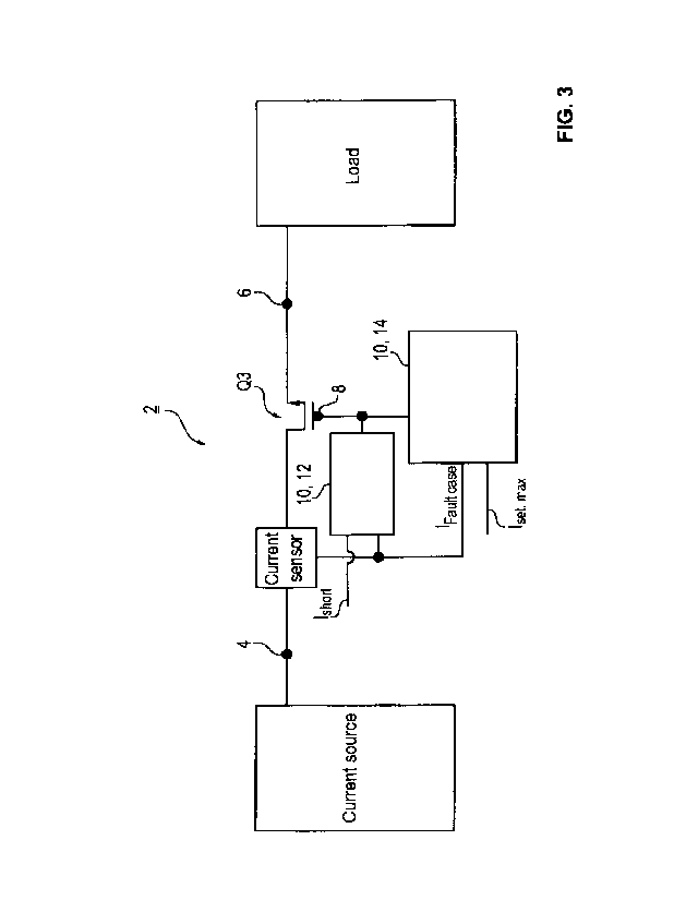
Fig. 3 shows a between an electronic circuit breaker 2
with a first semiconductor switch Q3 which is connected
in a current path 3 between a voltage input 4 and a
load output 6. The control input 8 of the first
semiconductor switch Q3 is connected to a control
device 10, wherein the control device 10 has a shut-off
circuit 12, also referred to as a shut-off device 12,
and a current limiting circuit 14, also referred to as
a current limiting device 14. The shut-off circuit 12
in this case switches off the first semiconductor
switch Q3, implemented as a MOSFET (Metal Oxide
Semiconductor Field Effect Transistor, MOS transistor),
in particular in the event of a short circuit or when
required, wherein the shut-off takes place relatively
quickly with respect to a response time of a
conventional current limiting circuit.
In addition, for example, the current limiting circuit
14 is produced from comparatively inexpensive
components and has a comparatively stable control
behavior, in particular of the load current. As is
apparent, in particular in figures 6 and 8, due to the
relatively rapid switching off of the first
semiconductor switch Q3 only comparatively small
current peaks occur. The control device 10 thus allows
the use of MOSFETS which are only required to handle
relatively small current peaks, thereby reducing costs
and increasing reliability, for example with regard to
the control stability.
In this case, the first semiconductor switch Q3 is
switched off (switched to the current-limiting state)
as soon as its load current (output current) exceeds a
CA 03076956 2020-03-25
- 13 -
maximum value 'short, in particular representing a short-
circuit current. The first semiconductor switch Q3 is
then actuated in a current-limiting state, wherein the
current limiting circuit 14 limits the load current
'load, in particular its current intensity, in such a
way that the load current 'load, in particular its
current intensity, is increased gradually
(continuously, rising relatively slowly) from a minimum
value I., in particular zero, to a current intensity
up to a nominal setpoint Iset,max (Fig. 6). In Fig. 6 the
load current 'load is designated as 'd
As shown in Figs. 6 and 7, abnormalities in the supply
voltage and therefore, in particular, the input
voltage, which is designated in Fig. 7 as Input
Voltage, and the current peak when the electronic
circuit breaker 2 according to the invention is used,
are comparatively small in relation to abnormalities in
the supply voltage and the current peak when an
electronic circuit breaker in accordance with the prior
art is used (Figs. 1 and 2).
Fig. 4 shows a block circuit diagram of the electronic
circuit breaker 2. The load current 'load is recorded by
means of a current sensor H1 connected in the current
path 3 and output as an actual value 'actual representing
this load current 'load to the control device 10, in
particular to a first input (pin) 16 of a control unit
pC of the control device 10. The actual value 'actual is
in the form of a voltage or a voltage signal. In this
case, the current sensor H1 advantageously has a
switching speed which is such that relatively rapid
changes, for example in the event of a short circuit,
are detected (resolved) by means of this recorded
current. In the event of a short circuit, the actual
value 'actual exceeds the maximum value 'short, which in
particular is fed to a second input (pin) 18 of the
control unit pC, so that, for example, a disconnection
CA 03076956 2020-03-25
- 14 -
is triggered in the control unit pC and so that the
control unit pC, implemented as a microcontroller,
outputs a signal Off, for example a voltage, at its
first output 20 which preferably remains output
(applied) until the signal Off at the output is
switched off.
Alternatively, in a variant not shown in detail, the
actual value 'actual is fed to a first input of a second
operational amplifier implemented as a comparator, and
the maximum value 'short is fed to the second input of
the second operational amplifier. The output of the
second operational amplifier is then connected to an
input of the control unit pC. Thus, when the maximum
value 'short is exceeded by the actual value 'actual a
corresponding (control or voltage) signal is fed to
this input of the control unit pC.
The first output 20 is connected via a fourth
semiconductor switch Q4 to a second semiconductor
switch Q2 and in parallel to a switch S1 of an
adjustment element 22. The adjustment element 22 in
this case has a capacitor C2, which in a first switch
position of the switch Si is connected via a resistor
R9 to a second output 24 of the control unit pC
outputting the nominal setpoint value Iset,maxr and in a
second switch position of the switch S2 via a resistor
R10 to a reference potential.
In addition, a voltage input Vgate is connected via the
resistors R7 and R3 to the control input 8 (the gate)
of the first semiconductor switch Q3. By means of a
voltage applied to this voltage input Vgate and the
electrical resistors R7 and R3, the operating point of
the first semiconductor switch Q3 is adjusted.
By means of a diode Cl, which is connected in a current
path which runs between the gate (control input 8) and
CA 03076956 2020-03-25
- 15 -
the source of the first semiconductor switch Q3, the
voltage between the gate and source of the first
semiconductor switch Q3 is limited. By means of the
resistor R12 connected in parallel to the diode D1 the
gate of the first semiconductor switch Q3 is discharged
when no voltage is present in the circuit.
As a result of the signal Off, the second semiconductor
switch Q2 is switched to the conducting state, its
output 26 is coupled to the control input 8 of the
first semiconductor switch Q3 so that as a result, the
control input 8, implemented as a gate, of the first
semiconductor switch Q3 is discharged. The load current
'load is disconnected by means of the first
semiconductor switch Q3. This process is realized
within a relatively short period, typically 1-10 ps
(Fig. 6). In addition, in particular at the same time,
the signal is output to a switch Si. This switch is
therefore connected in such a way that the capacitor C2
is discharged via the resistor R10.
In summary, the first semiconductor switch Q3 is
actuated by means of the second semiconductor switch
Q2. The resistors R3, R5, R7, R11 and R12 here are used
to adjust the magnitude of the voltage applied to the
control input 8 of the first semiconductor switch Q3.
In accordance with an alternative design of the
electronic circuit breaker 2, this additionally has a
current path between the voltage input Vgate and the
control input (the base) of the second semiconductor
switch Q2. A resistor R13 is connected into this
current path. This current path is illustrated in Fig.
4 by a dash-dotted line. When the signal Off is output,
the fourth semiconductor switch Q4 is switched in such
a way, in particular into the conducting state, that
the first semiconductor switch Q3 is switched to the
off state. In particular, the fourth semiconductor
CA 03076956 2020-03-25
- 16 -
switch Q4 is switched to the conducting state so that
the voltage applied to the control input 8 of the first
semiconductor switch Q3 is correspondingly reduced.
After a prescribed time period, which is preferably
designed such that the capacitor C2 just completely
(fully) discharges, i.e. it corresponds to a discharge
time of the capacitor 02 via the resistor R10, the
signal Off is switched off, so that the switch Si is in
the first switch position again and the capacitor 02 is
consequently charged via the resistor R9.
The adjustment element 22 is connected to a first input
28 of an operational amplifier OP1 and outputs a
setpoint value 'set, which is represented by means of
the voltage applied to the capacitor 02, to this first
input 28. The actual value 'actual is fed to a, in
particular inverting, second input 30 of the
operational amplifier.
.
By means of the operational amplifier OP1 a difference
between actual value 'actual and setpoint value 'set is
thus formed. This difference is output from the
operational amplifier OP1 as control signal D. By means
of a third semiconductor switch Q1 and the resistors R4
and R8 an amplifier is formed for the (voltage) signal
D output by the operational amplifier OP1. The
amplitude (the magnitude) of the signal D is thereby
modified or adjusted (amplified) to an amplitude
suitable for operating the second semiconductor switch
Q2 and thus for actuating the first semiconductor
switch Q3.
As the capacitor 02 is charged via an electrical
resistor R10 the setpoint value Iset fed to the first
input 28 changes according to the state of charge of
the capacitor 02. This causes a corresponding, in
particular gradual, change in the signal D. The second
CA 03076956 2020-03-25
- 17 -
semiconductor switch Q2 is thus actuated in such a way,
in particular to a gradually less conductive (non-
conducting) state, that the first semiconductor switch
Q3 is gradually (continuously) switched to the
conducting state. In this way, the load current 'load
gradually increases until the actual value 'actual fed to
the first input 16 of the control unit pC corresponds
to the nominal setpoint value Iset,max. As shown in Fig.
8, this allows the period of time in which load current
'load increases to be determined (specified) by means of
a suitable choice of the resistance value (size of the
resistance) of the electrical resistor R9 and the
capacitance of the capacitor 02, in other words by an
appropriate design of the adjustment element 22. In
this figure the load current is designated by Id.
In addition, a capacitor Cl is connected in a current
path between the second input 30 of the operational
amplifier OP1 and its output. The capacitor Cl has a
capacitance which is suitable for preventing an
oscillation of the output signal of the operational
amplifier OP1 and hence in the current path 3.
In accordance with Fig. 4, the shut-off circuit 12
comprises in summary an electrical resistor R1 and the
electrical resistor R10, the fourth semiconductor
switch Q4, the switch Si, the control unit 110 and, if
applicable, the second operational amplifier. In
particular, by forming a constant current source with a
voltage applied to the current path 3 by means of the
electrical resistors R2 to R5 and the electrical
resistors R7 to R9, Rll and R12, by means of the
capacitors Cl and C2, by means of the operational
amplifier OP1, by means of the semiconductor switches
Ql, Q2 and Q3, by means of the diode D1, and by means
of the current sensor H1, the load current Iload is
advantageously regulated, in particular held constant.
CA 03076956 2020-03-25
- 18 -
In addition, the output signal of the operational
amplifier OP1 in the form of control signal D, which is
implemented in particular as an output voltage, is fed
to a third input 32 of the control unit pC so that by
means of this signal the control unit pC determines
whether a current limitation of the load current 'load
by means of the first semiconductor switch Q3 is still
taking place. To prevent thermal damage, in particular
of the first semiconductor switch Q3, the first
semiconductor switch Q3 is switched to the non-
conducting state (switched off) if the current limiting
has persisted for a specified duration since the
beginning of the current-limiting actuation, in
particular without interruption.
In addition a voltage Vioad applied to the load (Load)
is fed to a fourth input 34 of the control unit pC.
The processing sequence described above of the method
for operating the electronic circuit breaker 2 is
summarized in the flowchart of Fig. 5. It is also
apparent that the first semiconductor switch Q3 is also
actuated in the current-limiting state when the nominal
setpoint value Iset,max is exceeded by the actual value
'actual, but the maximum value 'short is not exceeded.
In summary, the electronic circuit breaker 2 has a
first semiconductor switch Q3, preferably an N-channel
MOS transistor, which is connected in a current path 3
between a voltage input 4 and a load output 6. In
addition, the electronic circuit breaker 2 has a
control device 10 connected to the control input 8 of
the first semiconductor switch Q3, wherein the first
semiconductor switch Q3 is activated as a function of
an actual value 'actual of the load current 'load which is
fed to the control device 10. According to one
advantageous refinement, the control device 10 has a
control unit pC.
CA 03076956 2020-03-25
- 19 -
In an advantageous design, the electronic circuit
breaker also has a current sensor H1, which is
preferably connected in the current path 3.
In an advantageous design, the control device 10 has a
device and/or a circuit 14 for current limiting, and a
device and/or a circuit 12 for switching off or
blocking the current of the first semiconductor switch
Q3.
In a further advantageous design the first
semiconductor switch Q3 is actuated as a function of an
actual value 'actual of the load current 'load which is
fed to the control device 10, the current-limiting
device or circuit 14 and/or the shut-off device or
circuit 12.
In accordance with a suitable design of the electronic
circuit breaker, in the event of a short circuit and/or
if a maximum value 'short is exceeded by the actual value
1 actual r the control device 10 or the control unit pC
outputs a signal Off, in particular a shut-off signal,
to the current-limiting device or circuit 14 and/or
preferably to the shut-off device or circuit 12, to
disable and/or switch off the first semiconductor
switch Q3.
In a further advantageous design of the electronic
circuit breaker the actual value 'actual is fed to the
input side of the control device 10 or the current-
limiting device or circuit 14 and/or a nominal setpoint
value Iset,max is fed to the input side of the current-
limiting device or circuit 14, in particular by the
control unit pC.
In a further advantageous design, as a function of the
actual value 'actual and/or the nominal setpoint value
CA 03076956 2020-03-25
- 20 -
I set, max the first semiconductor switch Q3 is or will be
actuated in a current-limiting state.
In accordance with a suitable refinement, the control
device 10 and/or the current-limiting device or circuit
14 has an adjustment element 22. The nominal setpoint
value Iset,max is fed in a suitable manner to the input
side of the adjustment element 22 and it outputs a
setpoint value 'set at the output.
In a suitable design, the control device 10 or the
adjustment element 22 has a capacitor 02. The capacitor
02 is advantageously coupled by means of a switch Si to
the control device 10, in particular to the control
unit pC, or is discharged by means of the switch Si.
In another advantageous configuration, the control
device 10 or the current-limiting 14 device or circuit
14 has an operational amplifier OP1. Advantageously the
adjustment element 22 is connected to a first input 28
of the operational amplifier OP1 to feed in the
setpoint value 'set, and the actual value 'actual is fed
to a second input of the operational amplifier OP1. By
means of the operational amplifier OP1 a control signal
D, in particular, a difference between the setpoint
value 'set and the actual value 'actual/ is advantageously
formed to actuate the first semiconductor switch Q3. In
addition, in a suitable manner a load voltage Vioad is
fed to the control device 10 or the control unit pC.
In an advantageous design, the control device 10, the
current-limiting device or circuit 14 and/or the shut-
off device or circuit 12 has a second semiconductor
switch Q2, preferably a pnp bipolar transistor. In an
advantageous design the second semiconductor switch Q2
is connected to the control input 8 of the first
semiconductor switch Q3. In a further suitable design
the output 26 of the second semiconductor switch Q2
CA 03076956 2020-03-25
- 21 -
preferably forms an output of the current-limiting
device or circuit 14 and/or of the shut-off device or
circuit 12.
In an appropriate design the drain of the first
semiconductor switch Q3 is preferably connected to the
voltage input 4, the source is preferably connected to
the load output 6 and the gate to the control device
10.
In the method for operating the electronic circuit
breaker 2, in one of the above-mentioned variants
having a first semiconductor switch Q3 connected
between a voltage input 4 and a load output 6, in
accordance with the method an actual value 'actual of the
load current 'load or said current is recorded as an
actual value 'actual, in the event of a short circuit
when a maximum value 'short is exceeded by the actual
value 'actual the first semiconductor switch Q3 is
switched to the non-conducting state, and/or in the
event of an overload, on a setpoint 'set being exceeded
by the actual value 'actual the first semiconductor
switch Q3 is switched to a current-limiting state.
In an advantageous variant of the method, in the event
of a short circuit the setpoint value 'set of the load
current 'load is set to a minimum value Inun and then
increased continuously to a nominal setpoint value
(Iset,max) = Advantageously, a difference (difference
value) is formed from the actual value 'actual and the
setpoint 'set. Advantageously the difference (difference
value) is used as a control signal D for the current-
limiting actuation of the first semiconductor switch
Q3. The actuated first semiconductor switch Q3 actuated
in the current-limiting state is appropriately switched
into a non-conducting state and/or controlled after
expiry of a specified period and/or a specified timer
element.
CA 03076956 2020-03-25
- 22 -
The invention is not limited to the exemplary
embodiment described above. Instead, other variants of
the invention can also be derived from them by the
person skilled in the art, without departing from the
subject-matter of the invention. In particular, all
individual features described in connection with the
exemplary embodiments can also be combined together in
different ways without departing from the subject
matter of the invention.
CA 03076956 2020-03-25
- 23 -
List of reference signs
2 electronic circuit breaker
3 current path
4 voltage input
6 load output
8 control input
control device
12 shut-off device
10 14 current limiting device
16 first input to the control unit
18 second input to the control unit
first output of the control unit
22 adjustment element
15 24 second output of the control unit
26 output of the second semiconductor switch
28 first input of the operational amplifier
second input of the operational amplifier
32 third input to the control unit
20 34 fourth input to the control unit
Cl capacitor
02 capacitor
control signal/difference
25 D1 diode
H1 current sensor
actual actual value
'load load current
= minimum value
30 'set setpoint value
I set, max nominal setpoint value
short maximum value
pC control unit
Off shut-off signal
OP1 operational amplifier
Ql third semiconductor switch
Q2 second semiconductor switch
Q3 first semiconductor switch
CA 03076956 2020-03-25
- 24 -
Q4 fourth semiconductor switch
R1 to R13 electrical resistors
Vioad load voltage
Vgate voltage input