Note: Descriptions are shown in the official language in which they were submitted.
MEMORY CIRCUIT WITH ANALOG BYPASS PORTION
RELATED APPLICATIONS
[0001] This application claims priority from U.S. Patent Application
Serial
No. 15/851264, filed 21 December 2017, which issued as U.S. Patent No.
10,417,136.
TECHNICAL FIELD
[0002] This disclosure relates generally to classical and quantum
computing systems, and
more specifically to a memory circuit with an analog bypass portion.
BACKGROUND
[0003] Memory is a fundamental aspect of computing technology. The
ability to store
data in random-access memory (RAM) is essential to the capability of a
computer to perform
calculations, particularly in an ever increasing demand of faster
computational speeds. RAM is a
form of computer data storage which stores frequently used program
instructions and program
data to increase the general speed of a system. A RAM device allows data items
to be read or
written in almost the same amount of time irrespective of the physical
location of data inside the
memory. Typically, a given RAM is arranged as an array of rows and columns
that are accessed
by peripheral circuitry to write data to a particular row in a write
operation, and to subsequently
read the data from the row in a read operation. As an example, superconducting
digital
technology has provided computing and/or communications resources that benefit
from
unprecedented high speed, low power dissipation, and low operating
temperature. For decades,
superconducting digital technology has lacked RAM with adequate capacity and
speed relative to
logic circuits.
SUMMARY
[0004] One example includes a memory circuit. The circuit includes a
memory array
arranged as rows and columns of memory cells. An may portion stores a
respective memory
word in a given one of the rows in response to a word-write signal
corresponding to a write
1
Date Recue/Date Received 2021-09-13
CA 03077398 2020-03-27
WO 2019/125782 PCT1US2018/064320
address of the given one of the rows and in response to a plurality of bit-
write signals associated
with the plurality of columns, and reads a respective memory word from a given
one of the rows
in response to a word-read signal corresponding to a read address of the given
one of the rows
and in response to a plurality of bit-read signals associated with the
plurality of columns. The
circuit also includes a write-through detection system that activates an
analog bypass portion to
read the memory word from the analog bypass portion in response to the read
address being
equal to the write address.
[0005] Another example includes a method for reading data from a memory
array during
a write operation. The memory array includes rows and columns of memory cells.
The method
includes providing a write address signal corresponding to a write address of
the given one of the
rows and providing a word-write signal associated with the write address via a
write address
decoder to activate the respective one of the rows during a write operation.
The method also
includes providing a plurality of bit-write signals associated with the
respective columns of the
memory array to store a memory word in the respective one of the rows during
the write
operation and providing a read address signal corresponding to a read address
of a respective one
of the rows during the write operation. The method also includes comparing the
read address
signal and the write address signal and activating an analog bypass portion of
the memory array
in response to the read address signal being equal to the write address
signal. The method further
includes reading the memory word from the analog bypass portion of the memory
array in
response to activation of the analog bypass portion.
[0006] Another example includes a memory circuit. The circuit includes a
memory array
comprising an array portion and an analog bypass portion. The array portion
includes rows and
columns of memory cells. Each of the memory cells includes a superconducting
hysteretic
memory element and each of a plurality of cells of the analog bypass portion
comprising a
superconducting read element, the array portion storing a respective memory
word in a given one
of the rows in response to a word-write signal corresponding to a write
address of the given one
of the rows and in response to a plurality of bit-write signals associated
with the plurality of
columns, and to read a respective memory word from a given one of the rows in
response to a
2
CA 03077398 2020-03-27
WO 2019/125782 PCT1US2018/064320
word-read signal corresponding to a read address of the given one of the rows
and in response to
a plurality of bit-read signals associated with the plurality of columns. The
system further
includes a write-through detection system that activates the analog bypass
portion to read the
plurality of bit-write signals corresponding to the memory word from the
analog bypass portion
in response to the read address being equal to the write address.
BRIEF DESCRIPTION OF THE DRAWINGS
[0007] FIG. 1 illustrates an example of a memory circuit.
[0008] FIG. 2 illustrates another example of a memory circuit.
[0009] FIG. 3 illustrates an example of a memory cell.
[0010] FIG. 4 illustrates an example of an analog bypass cell.
[0011] FIG. 5 illustrates an example of a method for reading data from a
memory array
during a write operation.
DETAILED DESCRIPTION
[0012] This disclosure relates generally to classical and quantum
computing systems. and
more specifically to a memory circuit with an analog bypass portion. The
memory circuit
includes an array of memory cells arranged in contiguous rows and columns. The
array of
memory cells of the memory circuit are arranged as including an array portion
and an analog-
bypass portion. The array portion includes the memory cells arranged in a set
of rows and
columns, and is configured to store a memory word in a given one of the rows
in response to a
word-write signal corresponding to a write address of the given one of the
rows and in response
to a plurality of bit-write signals associated with the plurality of columns
during a write
operation. The array portion is also configured to facilitate reading a
respective memory word
from a given one of the rows in response to a word-read signal corresponding
to a read address
of the given one of the rows and in response to a plurality of bit-read
signals associated with the
plurality of columns during a read operation. The memory circuit also includes
a write-through
detection system that activates the analog bypass portion to read the memory
word from the
3
CA 03077398 2020-03-27
WO 2019/125782 PCT1US2018/064320
analog bypass portion in response to the read address being equal to the write
address, such as
during a write operation.
[0013] As an example, during a write operation, the write-through detection
system can
compare a write address signal corresponding to the write address and a read
address signal
corresponding to a read address that may be received at approximately the same
time. In
response to detecting that the write address and the read address are the same
(e.g.,
corresponding to the same row, such as based on the write and read address
signals being
approximately the same), the write-through detection system can command
deactivation of an
associated read address decoder to prohibit the read address decoder from
reading the row
corresponding to the read address signal. Additionally, the write-through
detection system can
command activation of the analog bypass portion, such as by providing a write-
through detection
signal to the analog bypass portion. Thus, the analog bypass portion can read
the memory word
based on reading the bit-write signals that are provided through the cells of
the analog bypass
portion. Accordingly, the memory circuit can allow reading a memory word
approximately
concurrently with the writing of the respective memory word to the memory
array.
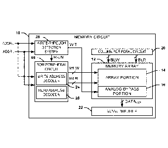
[00141 FIG. 1 illustrates an example of a memory circuit 10. The memory
circuit 10 can
be implemented in any of a variety of computer systems. such as a quantum
computer system.
For example, the memory circuit 10 can be implemented in a reciprocal quantum
logic (RQL)
computer system.
[00151 The memory circuit 10 includes a memory array 12 that is
demonstrated as
including an array portion 14 and an analog bypass portion 16. The array
portion 14 includes
memory cells that are arranged in an array of rows and columns. Each of the
rows of the array
portion 14 is configured to store a data word during a write operation in
response to a word-write
signal WLW that is generated from a row peripheral circuit 18 and selects the
respective row for
writing, and a plurality of bit-write signals BLW that are generated from a
column peripheral
circuit 20 and are each associated with a respective column of the array
portion 14. As an
example, the bit-write signals BLW can sequentially propagate through the rows
from the
column peripheral circuit 20. The data that is stored in the array portion 14
can be accessed
4
CA 03077398 2020-03-27
WO 2019/125782 PCT1US2018/064320
during a read operation in response to a word-read signal WLR that is
generated from the row
peripheral circuit 18 and selects the respective row for reading, and a
plurality of bit-read signals
BLR that are generated from the column peripheral circuit 20. Accordingly, a
data word that is
read from a respective row of the array portion 12 that is selected via a word-
read signal WLR
can be provided as output data DATA0uT in response to the bit-read signals
BLR. In the
example of FIG. 1, the output data DATAour is provided to a sense amplifier 22
that is
configured to provide the output data DATAour as the memory word that is read
from the
associated row of the array portion 14. As an example, the output data DATAour
can
correspond to the set of bit-read signals BLR in either a voltage state or a
non-voltage state, as
described in greater detail herein.
[0016] In the example of FIG. 1, the memory circuit 10 receives a write
address signal
ADDRw corresponding to a write address, and thus corresponding row, of the
array portion 14 to
which a memory word is to be written during the write operation. Similarly,
the memory
circuit 10 receives a read address signal ADDRR corresponding to a read
address, and thus
corresponding row, of the array portion 14 from which a memory word is to be
read during the
read operation. The row peripheral circuit 18 includes a write address decoder
24 that is
configured to determine the write address from the write address signal ADDRw
and to provide
the word-write signal WLW to the associated row during the write operation to
activate the
respective row of the array portion 14 for writing the respective memory word
to the respective
row via the bit-write signals BLW. Similarly, the row peripheral circuit 18
includes a read
address decoder 26 that is configured to determine the read address from the
read address signal
ADDRR and to provide the word-read signal WLR to the associated row during the
read
operation to activate the respective row of the array portion 14 for reading
the respective
memory word from the respective row via the bit-read signals BLR.
[0017] Additionally, the memory circuit 10 includes a write-through
detection system 28.
As an example, the memory circuit 10 can receive a command to write a memory
word to the
memory array 12 and a command to read a memory word from the array 12
approximately
concurrently in time. For example, an associated processor (not shown) can
require access to the
CA 03077398 2020-03-27
WO 2019/125782 PCT1US2018/064320
data that is requested to be read substantially immediately before or after it
commanded storage
of the data to the memory circuit 10, such as based on addressing stored in a
content addressable
memory (CAM). If the memory word that is to be read is stored in a row of the
array portion 14
of the memory array 12 to which the same memory word is being written, then a
timing error can
occur, such as resulting from the memory word that is read having not been
completely written
to the same row of the array portion 14. Accordingly, such a timing error can
result in a data
error of the memory word that is read from the row of the array portion 14.
[0018] To substantially mitigate timing errors associated with a
substantially concurrent
write operation and read operation from the same row of the array portion 14,
the write-through
detection system 28 is configured to likewise receive the write address signal
ADDRw and the
read address signal ADDRR. The write-through detection system 28 can thus
compare the write
address signal ADDRw and the read address signal ADDRR. In response to the
write address
signal ADDRw and the read address signal ADDRR being unequal, the write-
through detection
system 28 can provide a read-enable signal R-EN to command the row peripheral
circuit 18 to
allow access to the respective separate rows corresponding to the write
address signal ADDRw
via the word-write signal WLW and the read address signal ADDRR via the word-
read signal
WLR. However, if the write-through detection system 28 determines that the
write address
signal ADDRw and the read address signal ADDRR are equal, and thus the row to
which the
write address signal ADDRw is commanding a data word to be written is equal to
the row from
which the read address signal ADDRR is commanding a data word to be read, the
write-through
detection system 28 can activate the analog bypass portion 16 via a write-
through signal W-T,
such that the data word can be read from the analog bypass portion 16
substantially concurrently
with the writing of the data word to the row corresponding to the write
address signal ADDRw.
As an example, the write-through detection system 28 can also de-assert the
read-enable signal
R-EN to deactivate the read address decoder 26 R-EN to prohibit the read
address decoder 26
from generating the word-read signal WLR.
[0019] As an example, the analog bypass portion 16 can include a plurality
of cells that
zire arranged substantially similar to the memory cells of the array portion
14, except, as an
6
CA 03077398 2020-03-27
WO 2019/125782 PCT1US2018/064320
example, the cells of the analog bypass portion 16 may not include a
hysteretic memory element.
For example, the memory circuit 10 can be implemented in a quantum or
quantum/classical
computer system, such that each of the memory cells of the array portion 14
can include a
superconducting hysteretic memory clement (e.g., a hysteretic magnetic
Josephson junction). In
the example of a quantum computer system, each of the cells of the analog
bypass portion 16 can
include a superconducting read element (e.g., a superconducting quantum
interference device
(SQUID)) that is activated by a write-through signal W-T that is provided by
the write-through
detection system 28 to activate the analog bypass portion 16.
[0020] As an example, the cells of the analog bypass portion 16 can be
coupled to bit-
write lines on which the bit-write signals BLW are provided. As a result, in
response to
activation of the analog bypass portion 16 via the write-through signal W-T,
the cells of the
analog bypass portion 16 can read the memory word that is being written to the
row
corresponding to the write address signal ADDRw via the bit-write signals BLW
likewise
directly from the bit-write signals BLW. In other words, as an example,
because the bit-write
signals BLW correspond to the memory word that is written to the row
corresponding to the
write address signal ADDRw, the bit-write signals BLW can likewise be read
directly from the
analog bypass portion 16 (e.g., via activation by the write-through signal W-
T) as the bit-write
signals BLW propagate through the memory array 12. Accordingly, the memory
word can be
read from the memory array 12 substantially concurrently with the writing of
the memory word
to the memory array 12 in a manner that substantially mitigates the risk of
timing errors that can
affect the integrity of the memory word. As a result, the memory circuit 10
can operate in a
much quicker and more efficient manner by not be required to wait until
conclusion of a write
operation before initiating a read operation based on allowing a data word to
be read from the
memory array 12 concurrently with the same data word being written to the
memory array 12.
[0021] FIG. 2 illustrates another example of a memory circuit 50. The
memory circuit 50
can include components that are included in the memory circuit 10 in the
example of FIG. 1.
Therefore, reference is to be made to the example of FIG. 1 in the following
description of the
example of FIG. 2.
7
CA 03077398 2020-03-27
WO 2019/125782 PCT1US2018/064320
[0022] The memory circuit 50 includes a memory array 52 that is
demonstrated as
including an array portion 54 and an analog bypass portion 56. As an example,
the memory
array 52 can be configured substantially similar to as described previously in
the example of
FIG. 1. The array portion 54 includes memory cells that are arranged in an
array of rows and
columns. Each of the rows of the array portion 54 is configured to store a
data word during a
write operation in response to a word-write signal WLW (not shown) that is
generated from the
row peripheral circuit (not shown) and selects the respective row for writing,
and a plurality of
bit-write signals BLW that are generated from a column peripheral circuit (not
shown) and are
each associated with a respective column of the array portion 54.
[0023] In the example of FIG. 2, the memory circuit 50 also includes a
write-through
detection system 58 that receives a write address signal ADDRw corresponding
to a write
address during a write operation and receives a read address signal ADDRR
corresponding to a
read address during a read operation. The memory circuit 50 is also
demonstrated as including a
read address decoder 60, such as arranged as part of a row peripheral circuit,
that is configured to
determine the read address from the read address signal ADDRR and to provide
the word-read
signal WLR to the associated row during the read operation to activate the
respective row of the
array portion 54 for reading the respective memory word from the respective
row (e.g., via the
bit-read signals (not shown)). As described in greater detail herein, the
memory circuit 50 also
includes an enable signal EN (e.g., from an external processor) during a read
operation to
facilitate reading the requested memory word from the memory array 52.
[0024] In the example of FIG. 2, the write-through detection system 58
includes a
comparator 64 is configured to likewise receive the write address signal ADDRw
and the read
address signal ADDRR. The comparator 64 can be configured as a digital
comparator to
compare the write address signal ADDRw and the read address signal ADDRR. The
comparator 64 provides a control signal CTRL as an output having a logic-state
that is based on
the comparison. In response to the write address signal ADDRw and the read
address signal
ADDRR being equal, the comparator 64 can assert a control signal CTRL.
Alternatively, in
8
CA 03077398 2020-03-27
WO 2019/125782 PCT1US2018/064320
response to the write address signal ADDRw and the read address signal ADDRR
being unequal,
the comparator 64 can de-assert a control signal CTRL.
[0025] The control signal CTRL and the enable signal EN are each provided
to a set of
logic gates that are arranged as part of the write-through detection system
58. In the example of
FIG. 2, the logic gates include a first AND-gate 66 that is configured to
perform a logic-AND
operation on the enable signal EN and the inverted control signal CTRL to
generate the read
enable signal R-EN. Therefore, while the control signal CTRL is de-asserted
based on an
unequal condition between the write address signal ADDRw and the read address
signal ADDRR,
the read enable signal R-EN is provided to the read address decoder 60 to
enable the read address
decoder 60(0 generate the word-read signal WLR in response to the read address
signal ADDRR.
However, in response to the control signal CTRL being asserted based on the
write address
signal ADDRw and the read address signal ADDRR being equal, the read enable
signal R-EN is
de-asserted to deactivate the read address decoder 60. As a result, the read
address decoder
ceases to produce the word-read signal WLR associated with the respective row
in the array
portion 54 in response to the read address signal ADDRR.
[0026] In addition, the logic gates include a second AND-gate 68 that is
configured to
perform a logic-AND operation on the enable signal EN and the control signal
CTRL to generate
the write-through signal W-T. Therefore, while the control signal CTRL is de-
asserted based on
an unequal condition between the write address signal ADDRw and the read
address signal
ADDRR, the write-through signal W-T is de-asserted, and thus the analog bypass
portion 56 is
deactivated. However, in response to the control signal CTRL being asserted
based on the write
address signal ADDRw and the read address signal ADDRR being equal, the write-
through signal
W-T is asserted to activate the analog bypass portion 56. As a result, the
requested memory
word can be read from the analog bypass portion via the bit-write signals BLW,
as opposed to
from the respective row corresponding to the read address signal ADDRR. Thus,
the data states
of the bit-write signals BLW can collectively correspond to the output data
DATAour, such as
provided to the sense amplifier (not shown), as read from the activated analog
bypass portion 56.
Accordingly, reading the memory word from the analog bypass portion 56
concurrently with the
9
CA 03077398 2020-03-27
WO 2019/125782 PCT1US2018/064320
same memory word being written to the array portion 54 can provide for a more
rapid manner of
accessing the data from the memory array 52 in a manner that substantially
mitigates errors.
[0027] FIG. 3 illustrates an example of a memory cell 100. As an example,
the memory
cell 100 can correspond to one of a plurality of memory cells that are
arranged in the rows and
columns of the memory arrays 12 and/or 52. Therefore, reference is to be made
to the examples
of FIGS. 1 and 2 in the following description of the example of FIG. 3.
[0028] The memory cell 100 includes a word-write line 102 and a word-read
line 104
that each pass through the memory cell 100. The word-write line 102 conducts a
word-write
signal WLW during a write operation and the word-read line 104 conducts a word-
read signal
WLR during a read operation. As an example, the word-write signal WLW and the
word-read
signal WLR can each be provided as a current. For example, the word-write
signal WLW can
correspond to a word-write signal associated with a row of memory cells in the
array portion 54
of the memory array 52, and the word-read signal WLR can correspond to a word-
read signal
associated with the row of memory cells in the array portion 54 of the memory
array 52. For
example, the word-write and word-read lines 102 and 104 can likewise be
coupled to adjacent
memory cells in a given row on either side of the memory cell 100. Thus, the
word-write signal
WLW and the word-read signal WLR propagate through all of the memory cell
systems in the
row, including the memory cell 100, during the respective write and read
operations.
[0029] Similarly, the memory cell 100 includes a bit-write line 106 and a
bit-read
line 108 that each pass through the memory cell 100. The bit-write line 106
conducts a bit-write
signal BLW during the write operation and the bit-read line 108 conducts a bit-
read signal BLR
during the read operation. As an example, the bit-write signal BLW and the bit-
read signal BLR
can each be provided as a current. For example, the bit-write signal BLW can
correspond to a
bit-write signal associated with a column of memory cells in the array portion
54 of the memory
array 52, and the bit-read signal BLR can correspond to a bit-read signal
associated with the
column of memory cells in the array portion 54 of the memory array 52. In a
similar manner, the
second write and second read lines 106 and 108 can likewise be coupled to
adjacent memory
cells in a given column above and below the memory cell 100. Thus, the bit-
write signal BLW
CA 03077398 2020-03-27
WO 2019/125782 PCT1US2018/064320
and the bit-read signal BLR propagate through all of the memory cell systems
in the column,
including the memory cell 100, during the respective write and read
operations. As an example,
the bit-read line 108 associated with each of the memory cells 100 in a given
column can be
coupled to the sense amplifier 22, such that the sense amplifier 22 can read
the logic-state of the
memory cell 100 during a read operation.
[WM The memory cell 100 also includes a superconducting hysteretic
memory element,
demonstrated in the example of FIG. 3 as a phase hysteretic magnetic Josephson
junction
(PHMJJ) 110, that is configured to store a digital state corresponding to one
of the binary logic-1
state or the binary logic-0 state. As an example, the PHMJJ 110 can include
ferromagnetic
materials in associated barriers to be configured as a switchable 7c-junction.
The memory
cell 100 also includes a first Josephson junction J1 and a second Josephson
junction J2 that are
arranged in parallel with the PHMJJ 110, and which collectively form a
superconducting
quantum interference device (SQUID). As an example, the Josephson junctions Ji
and J2 can be
configured as superconductor-ferromagnetic-superconductor (SFS) Josephson
junctions. The
PHMJJ 110 can include outer layers of superconducting material, such as
Niobium (Nb), and one
or more internal thin film layers of ferromagnetic materials. As an example,
the thin film layers
of ferromagnetic materials can include one or more "hard" ferromagnetic layers
having a
substantially fixed magnetic field and one or more "soft" ferromagnetic layers
that can be
changed as a result of magnetic fields generated locally by orthogonal
electrical currents.
Furthermore, the PHMJJ 110 can include one or more additional layers, such as
oxide layers, that
are interleaved with the superconducting and/or ferromagnetic layers.
[0031] In the example of FIG. 3, the word-write line 102 and the bit-write
line 106 are
demonstrated as magnetically coupled to the PHMJJ 110, as indicated at 106. As
an example,
the PHMJJ 110 can include two or more different ferromagnetic layers, and the
orientation of the
magnetic field in one of the ferromagnetic layers is substantially fixed. The
magnetic field
orientation of the other one or more ferromagnetic layers can be changed as a
result of magnetic
fields that are generated locally by the word-write signal WLW and the bit-
write signal BLW.
11
CA 03077398 2020-03-27
WO 2019/125782 PCT1US2018/064320
[00321 Therefore, based on the configuration of the PHMJJ 110, the word-
write signal
WLW and the bit-write signal BLW can generate the magnetic field to set the
digital state of the
PHMJJ 110 to a binary logic-1 state or a binary logic-0 state using magneto-
current states of the
PHMJJ 110 based on the respective directions of signal propagation during a
write operation. As
one example, if the combined magnetic field produced by the word-write signal
WLW and the
bit-write signal BLW has the same orientation as the internal magnetic field
of the hard
ferromagnetic layers, the individual magnetic fields of each of the word-write
signal WLW and
the bit-write signal BLW can add together positively or negatively to set the
digital state of the
phase hysteretic magnetic Josephson junction to correspond to a binary logic-1
state or a binary
logic-0 state respectively. However, if the combined magnetic field produced
by the word-write
signal WLW and the bit-write signal BLW has the opposite orientation as the
internal magnetic
field of the hard ferromagnetic layers, the digital state of the PHMJJ 110
remains unchanged. As
another example, the word-write signal WLW and the bit-write signal BLW can be
applied as a
sequence of write signal pulses, such that if the word-write signal WLW
overlaps in time with
the bit-write signal :BLW, the digital state of the PHMJJ 110 can correspond
to a binary logic-1
state or a binary logic-0 state. However, if only one such pulse is present at
a given time, or if
the word-write signal and bit-write signal WLW and WLR do not sufficiently
overlap in time,
the digital state of the PHMJJ 110 can remain unchanged.
[0033] Similarly, the individual magnetic field of only one of the word-
write signal
WLW and the bit-write signal BLW may be insufficient to change the digital
state of the
PHMJJ 110, such that memory cells in unaddressed rows maintain their
respective digital states
despite the propagation of the bit-write signal BLW. Furthermore, based on the
superconductivity of the word-write line 102 and the bit-write line 106 and
the presence of a
superconducting ground plane, cross coupling between the word-write line 102
and the bit-write
line 106 can be substantially mitigated. Therefore, for a given propagation
direction of the word-
write signal WLW in a given row, the propagation directions of the respective
bit-write signals
BLW in each of the columns can be controlled to set the digital state of each
of the PHMJJs 102
12
CA 03077398 2020-03-27
WO 2019/125782 PCT1US2018/064320
in a given row during a write operation without affecting the digital states
in any of the memory
cells in any of the other rows through which a word-write signal WLW is not
provided.
[0034] In the example of FIG. 3, the memory cell 100 includes a transformer
112 that
includes a primary winding Li on the word-read line 104 through which the word-
read signal
WLR propagates. The transformer 112 also includes a secondary winding L2
inductively
coupled to the primary winding Li and arranged in parallel with the PHMJJ 110
and with the
Josephson junctions J1 and J2. Therefore, the word-read signal WLR is
inductively provided to
the Josephson junctions Ji and J-). The bit-read line 108 is coupled to a node
114 that is coupled
to the secondary winding L.?, such that the bit-read signal BLR enters the
memory cell 100 at the
node 114, and is coupled to a node 116 corresponding to an output of the
memory cell 100
between the Josephson junctions Ji and J2, such that the bit-read signal BLR
exits the memory
cell 100 from the node 114.
100351 The digital state of the PHMJJ 110 can be read from the memory cell
1(X) in
response to the word-read signal WLR and the bit-read signal BLR.
Specifically, the word-read
signal WLR can be provided on the word-read line 104 to select the row of
memory cells in the
associated memory array 52. As an example, the word-read signal WLR propagates
through the
primary winding Li of the transformer 112 as a DC current pulse. The DC
current pulse of the
word-read signal WLR is inductively provided to the PHMJJ 110 and the
Josephson junctions Ji
and J2. Therefore, the current induced by the word-read signal WLR via the
secondary winding
L2 is added to the bit-read signal BLR based on the direction of propagation
of the word-read
signal WLR. The stored binary digital state of the PHMJJ 110 can be
determinative of the
critical current necessary to trigger the Josephson junctions Ji and J2 based
on the
superconducting phase that can be provided by the PHMJJ 110.
100361 For example, if the PHMJJ 110 is in a zero state, and thus stores a
logic-0 binary
state, the PHMJJ 110 is in a substantially minimum Josephson energy ground
state that does not
provide superconducting phase. Therefore, the added magnitude of the bit-read
signal BLR and
the word-read signal WLR, as induced to the Josephson junctions J1 and J2, is
not sufficient to
trigger the Josephson junctions Ji and J2. Accordingly, a voltage on the bit-
read line 108 can
13
CA 03077398 2020-03-27
WO 2019/125782 PCT1US2018/064320
remain at a substantially decreased magnitude (e.g., zero volts) to indicate
the logic-0 state.
However, as another example, if the PHMJJ 110 is in a n-state, and thus stores
a logic-1 binary
state, the PHMJJ 110 has a substantially maximum Josephson energy and provides
a
superconducting phase that is added to the magnitude of the bit-read signal
BLR and the word-
read signal WLR. Therefore, the contribution of the superconducting phase, the
bit-read signal
BLR, and the word-read signal WLR, as induced to the Josephson junctions Ji
and J2, is
sufficient to trigger the Josephson junctions Ji and J2. Accordingly, the
Josephson junctions J1
and J2 can trigger in an oscillatory manner to increase the voltage on the hit-
read line 108 to
indicate the logic-1 state.
[0037] The memory cell 100 is demonstrated as but one example of a memory
cell that
can be provided in the memory arrays 12 and/or 52, as described herein. While
the memory
cell 100 demonstrates a superconducting hysteretic memory element that is
configured as a
PHMJJ, it is to be understood that other types of superconducting hysteretic
memory elements
can instead be implemented in the memory arrays 12 and/or 52, such as can
operate in different
ways. Additionally, it is to be understood that the memory arrays 12 and/or 52
are not limited to
including superconducting hysteretic memory elements, but can instead
implement non-
superconducting hysteretic memory elements. Therefore, the memory arrays 12
and/or 52 can be
configured with memory cells of any of a variety of different configurations.
[0038] FIG. 4 illustrates an example of an analog bypass cell 150. As an
example, the
analog bypass cell 150 can correspond to one of a plurality of analog bypass
cells that are
arranged in a row of the analog bypass portion 16 and/or 56 of the respective
memory arrays 12
and/or 52. As an example, the analog bypass cell 150 can he included the in
same memory
array 12 and/or 52 in which the memory cell 100 is included. Therefore,
reference is to be made
to the examples of FIGS. 1 and 2 in the following description of the example
of FIG. 4.
[0039] The analog bypass cell 150 includes a write-through line 152 that
passes through
the analog bypass cell 150. The write-through line 152 conducts a write-
through signal W-T,
such as generated by the write-through detection system 28 in the example of
FIG. 1 or the
second AND-gate 68 in the example of FIG. 2. As an example, the write-through
signal W-T
14
CA 03077398 2020-03-27
WO 2019/125782 PCT1US2018/064320
can be provided to the analog bypass cell 150 in response to the write-through
detection
system 28 and/or 58 detecting that the write address and the read address
(e.g., the write address
signal ADDRIN and the read address signal ADDRR) are equal. For example, the
write-through
signal W-T can be provided as a current. As an example, the write-through line
152 can be
coupled to adjacent analog bypass cells in the analog bypass portion 16 and/or
56 on either side
of the analog bypass cell 150. Thus, the write-through signal W-T propagates
through all of the
analog bypass cells in the analog bypass portion 16 and/or 56, including the
analog bypass
cell 150. Therefore, the write-through signal W-T can be provided to activate
the analog bypass
portion 16 and/or 56 to facilitate the memory word to be read from the analog
bypass portion 16.
Accordingly, the write-through signal W-T is provided through the analog
bypass cell 150 to
facilitate reading a single bit (e.g., a logic-state of the single bit) of the
memory word from the
analog bypass cell 150.
[0040] The analog bypass cell 150 also includes a bit-write line 156 and a
hit-read
line 158 that each pass through the analog bypass cell 150. As an example, the
bit-write line 156
and the bit-read line 158 can correspond to the bit-write line 106 and the bit-
read line 108 in the
example of FIG. 3. For example, the analog bypass portion 16 and/or 56 can
form a row of the
respective memory array 12 and/or 52, such as a last row (e.g., on a "bottom"
of the memory
array 12 and/or 52 opposite the column peripheral circuit 20). Therefore, the
bit-write line 156
and the bit-read line 158 can extend through each of the memory cells 100 in a
given column and
through the analog bypass cell 150. As an example, the bit-read line 158 can
be coupled to the
sense amplifier 22, such that the sense amplifier 22 can be configured to read
the memory word
from the analog bypass portion 16 and/or 56 based on reading each bit of the
memory word from
a respective one of the analog bypass cells 150.
[0041] The analog bypass cell 150 also includes a superconducting read
element,
demonstrated in the example of FIG. 4 as a SQUID 160. In the example of FIG.
4, the analog
bypass cell 150 includes a first Josephson junction J3 and a second Josephson
junction J4. The
Josephson junctions J3 and J4 are arranged in parallel with a first
transformer 162 that includes a
primary winding L3 and a secondary winding L. and a second transformer 164
that includes a
CA 03077398 2020-03-27
WO 2019/125782 PCT1US2018/064320
primary winding L5 and a secondary winding L6. As an example, the Josephson
junctions J3 and
J4 can be configured as superconductor-ferromagnetic-superconductor (SFS)
Josephson
junctions. The Josephson junctions J3 and J4 and the secondary windings L4 and
L6 thus form the
SQUID 160. As described herein, the SQUID 160 can be implemented to read a bit
of the
memory word from the analog bypass portion 16 and/or 56. Because the analog
bypass cell 150
includes a SQUID 160 that does not include a PHMJJ, as opposed to the memory
cell 100, the
analog bypass cell 150 can be fabricated in a much more compact and simplistic
manner than the
memory cells 100.
[0042] In the example of FIG. 4, the primary winding L3 is arranged on the
write-through
line 152 through which the write-through signal W-T propagates. Therefore, the
write-through
signal W-T is inductively provided to the Josephson junctions J3 and J4.
Similarly, in the
example of FIG. 4, the primary winding L5 is arranged on the bit-write line
156 through which
the bit-write signal BLW propagates. Therefore, the bit-write signal BLW is
likewise
inductively provided to the Josephson junctions J3 and J4. In the example of
FIG. 4, the bit-write
line 156 is demonstrated as grounded after the primary winding L5. However,
this is based on
the example of the analog bypass cell 150 being arranged at the "bottom" of
the memory array 12
and/or 52, and the bit-write line 156 could instead be coupled to or be
configured as the bit-write
line 106 of additional memory cells 100 in the associated column based on the
analog bypass
portion 16 and/or 56 corresponding to a different row (e.g., top or elsewhere)
in the memory
array 12 and/or 52. The bit-read line 158 is coupled to a node 166 that is
coupled to the
secondary windings L4 and L. such that the bit-read signal BLR enters the
analog bypass
cell 150 at the node 166, and is coupled to a node 168 corresponding to an
output of the analog
bypass cell 150 between the Josephson junctions J3 and J4, such that the bit-
read signal BLR
exits the analog bypass cell 150 from the node 166. As described previously,
the node 166 can
be coupled to the sense amplifier 22, such that the bit-read signal BLR can be
read by the sense
amplifier 22.
[0043] The digital state of the bit-write signal BLW can be read via the
SQUID 160 in
re9){12 to the bit-write signal BLW and the write-through signal W-T.
Specifically, the write-
16
CA 03077398 2020-03-27
WO 2019/125782
PCT1US2018/064320
through signal W-T can be provided on the write-through line 152 to select the
analog bypass
portion 16 and/or 56 in the associated memory array 52. The write-through
signal W-T
propagates through the primary winding L3 of the first transformer 162 as a DC
current pulse.
The DC current pulse of the write-through signal W-T is inductively provided
to the Josephson
junctions J3 and J4. As an example, the bit-write line BLW can have a positive
amplitude to
indicate a logic-1 state, and can have a zero amplitude to indicate a logic-0
state. Therefore, if
the bit-write line BLW has a zero amplitude, as induced to the Josephson
junctions J3 and J4, and
thus a logic-0 state, the added amplitude of the write-through signal W-T, as
induced to the
Josephson junctions J3 and J4, is not sufficient to trigger the Josephson
junctions J3 and J.
Accordingly, a voltage on the bit-read line 158 at the node 168 can remain at
a substantially
decreased magnitude (e.g., zero volts) to indicate the logic-0 state. However,
as another
example, if the bit-write line BLW has a positive amplitude, as induced to the
Josephson
junctions J3 and J4, and thus a logic-1 state, the added amplitude of the
write-through signal W-T,
as induced to the Josephson junctions J3 and J4, is sufficient to trigger the
Josephson junctions J3
and J4. Accordingly, the Josephson junctions J3 and J4 can trigger in an
oscillatory manner to
increase the voltage on the bit-read line 158 at the node 168 to indicate the
logic-1 state.
[0044]
Accordingly, the analog bypass cell 150 demonstrates a manner of reading the
memory word that is concurrently being written to a row in the array portion
14 and/or 54 (e.g.,
via the bit-write signals BLW). Particularly, in response to activation of the
analog bypass
portion 16 and/or 56 via the write-through signal W-T, the respective bit of
the memory word
that is being written to the row corresponding to the write address signal
ADDRw can be read
from the analog bypass cell 150 via the respective bit-write signal BLW. In
other words, as an
example, because the bit-write signal BLW corresponds to the respective bit of
the memory word
that is written to the row corresponding to the write address signal ADDRw,
the bit-write signal
BLW can likewise be read directly from the analog bypass cell 150 (e.g., via
the write-through
signal W-T) as the bit-write signal BLW propagates through the memory array 12
and/or 52
from the memory cells (e.g., the memory cells 100) in the column to the analog
bypass cell 150.
Accordingly, the memory word can be read from the memory array 12 and/or 52
substantially
17
CA 03077398 2020-03-27
WO 2019/125782 PCT1US2018/064320
concurrently with the writing of the memory word to the memory array 12 and/or
52 in a manner
that substantially mitigates the risk of timing errors that can affect the
integrity of the memory
word. As a result, the memory circuit 10 can operate in a much quicker and
more efficient
manner by not be required to wait until conclusion of a write operation before
initiating a read
operation based on allowing a data word to be read from the memory array 12
and/or 52
concurrently with the same data word being written to the memory array 12
and/or 52.
10045] In view of the foregoing structural and functional features
described above, a
method in accordance with various aspects of the present disclosure will be
better appreciated
with reference to FIG. 5. While, for purposes of simplicity of explanation,
the method of FIG. 5
is shown and described as executing serially, it is to be understood and
appreciated that the
present disclosure is not limited by the illustrated order, as some aspects
could, in accordance
with the present disclosure, occur in different orders and/or concurrently
with other aspects from
that shown and described herein. Moreover, not all illustrated features may be
required to
implement a method in accordance with an aspect of the present disclosure.
[00461 FIG. 5 illustrates a method 200 for reading data from a memory array
(e.g., the
memory array 12) during a write operation, the memory array comprising rows
and columns of
memory cells (e.g.. the memory cell 100). At 202, a write address signal
(e.g., the write address
signal ADDRw) corresponding to a write address of the given one of the rows is
provided.
At 204, a word-write signal (e.g., the word-write signal WLW) associated with
the write address
is provided via a write address decoder (e.g., the write address decoder 24)
to activate the
respective one of the rows during a write operation. At 206, a plurality of
bit-write signals (e.g.,
the bit-write signals B LW) associated with the respective columns of the
memory array are
provided to store a memory word in the respective one of the rows during the
write operation.
At 208, a read address signal (e.g., the read address signal ADDRR)
corresponding to a read
address of a respective one of the rows is provided during the write
operation. At 210, the read
address signal and the write address signal are compared. At 212, an analog
bypass portion (e.g.,
the analog bypass portion 16) of the memory array is activated in response to
the read address
18
CA 03077398 2020-03-27
WO 2019/125782 PCT1US2018/064320
signal being equal to the write address signal. At 214, the memory word is
read from the analog
bypass portion of the memory array in response to activation of the analog
bypass portion.
[0047] What have been described above are examples of the disclosure. It
is, of course,
not possible to describe every conceivable combination of components or method
for purposes of
describing the disclosure, but one of ordinary skill in the art will recognize
that many further
combinations and permutations of the disclosure are possible. Accordingly, the
disclosure is
intended to embrace all such alterations, modifications, and variations that
fall within the scope
of this application, including the appended claims.
19