Note: Descriptions are shown in the official language in which they were submitted.
CA 03078269 2020-04-02
WO 2019/072786 PCT/EP2018/077380
1
HIGH-VOLTAGE POWER SUPPLY SYSTEM
TECHNICAL FIELD OF THE INVENTION
The present invention relates to the field of electrical power
engineering and more specifically to the field of power supplies suitable for
supplying electrostatic precipitators (ESPs).
BACKGROUND OF THE INVENTION
Electrostatic precipitators (ESPs) are commonly used for collection and
removal of particulate matter from a gas stream in industrial processes.
These devices may for example be utilized to filter particulate from the
emissions of coal fired power plants, cement factories, steel plants and
refuse
incineration. Some of the reasons to as why ESPs are one of the more
frequently used devices for particulate filtering/collection is that they can
handle relatively large gas volumes with a wide range of inlet temperatures,
pressures, dust volumes and acid gas conditions. Moreover, they can be
used to collect a wide range of particle sizes and they can collect in dry and
wet states.
As implied by its name, an ESP uses electrostatic forces to separate
dust particles from the gas stream. A conventional ESP has a set of
discharge/emitting electrodes, often in the form of thin wires, which are
evenly
spaced between large plates called collection/collecting electrodes, the
emitting electrodes are charged with a high voltage while the collecting
electrodes are generally grounded but may be charged with a voltage of
opposite polarity. Commonly, a negative, high-voltage (oftentimes pulsating)
direct current (DC) is applied to the emitting electrode, creating a negative
electric field. In short, the flowing gases are arranged to pass through the
negative electric field provided by the emitting electrodes, causing the solid
particulate to be negatively charged. The negatively charged particles are
subsequently attracted to the collecting electrodes to which they adhere. By
shaking or knocking these collection plates, an accumulated mass of "dust" is
freed and caused to fall down, under its own weight, into a dust container
CA 03078269 2020-04-02
WO 2019/072786 PCT/EP2018/077380
2
(hopper) arranged underneath. In more detail, there are other steps in the
process such as avalanche multiplication and secondary emission which
ionize the gas molecules, which in turn ionize these solid particles and cause
a net result of negatively charged particles that are repulsed by the negative
electrical field around the emitting electrodes and strongly attracted to the
collecting electrode.
High-voltage pulse generators are commonly used in ESPs in order to
superimpose voltage pulses on a DC voltage and thereby increase the
particle separating or filtering performance. The pulse width typically is in
the
order of 100 ps and the frequency lies in the range of 1 to 400 pulses/s. The
average current can be controlled by varying the pulse repetition frequency of
a switching device in the system, while maintain the voltage level applied to
the electrostatic precipitator. In this way it is possible to eliminate or at
least
limit the generation of back corona and the negative effects associated
therewith.
The pulse systems are often divided into two main categories, one
which is based on switching at high potential/voltage (at the secondary side),
and one which will be referred to as pulse transformer systems which are
based on switching at low potential (at the primary side). Examples of the
latter, where switching takes places on the primary side, can be found in e.g.
US 4,052,177, US 4,600,411 and EP 1 652 586, while EP 1 293 253
discloses an example of high voltage switching (i.e. where the switching takes
place on the secondary side).
Document US 5,575,836 discloses a dust collector with a pulse power
supply. In this case, the switching 12 is arranged on the secondary side of a
transformer 10. However, it is quite clear that the switching is not performed
on the final voltage level. On the contrary, in US 5,575,836 a pulse
transformer 16 is required to increase the voltage up to the final level.
However, even though many prior art solutions exist there is always a
need for further improvements in the art, particularly for improvements in
terms of reduced power losses, reduced size, costs, reduced voltage ripple
on the output, and/or robustness/reliability.
CA 03078269 2020-04-02
WO 2019/072786
PCT/EP2018/077380
3
SUMMARY OF THE INVENTION
It is therefore an object of the invention to provide a high-voltage power
supply system for energizing an electrostatic precipitator, which alleviates
all
or at least some of the drawbacks associated with presently known systems
in terms of power loss, size, cost, reduced voltage ripple on the output
and/or
robustness/reliability.
This object is achieved by means of a high-voltage power supply
system as defined in the appended claims.
In the following, the term exemplary is to be understood as serving as
an example, instance or illustration.
According to a first aspect of the present invention, there is provided a
power supply system generating high-voltage pulses superimposed on a DC
base voltage suitable for powering an electrostatic precipitator. The high
voltage power supply system comprises an AC supply circuit configured to
generate a first AC supply voltage and a second AC supply voltage, a DC
supply circuit connectable (i.e. configured/adapted to be connected to)
between the AC supply circuit and the electrostatic precipitator, the DC
supply
circuit comprising a first transformer and a first rectifier circuit for
transforming
and converting the first AC supply voltage to the DC base voltage and a pulse
supply circuit connectable between the AC supply circuit and the electrostatic
precipitator. The pulse supply circuit comprises a second transformer and a
second rectifier circuit for transforming and converting the second AC supply
voltage to a DC pulse supply voltage, sufficient to generate the high-voltage
pulses, and a pulse forming circuit connectable between the second rectifier
circuit and the electrostatic precipitator, where the pulse forming circuit is
configured to generate (and forward/supply) high-voltage pulses without
additional voltage transformation. More specifically, the AC supply circuit is
configured such that a frequency of each of the first AC supply voltage and
the second AC supply voltage are in the range of 100 Hz to 5000 Hz.
Hereby, a cost effective and compact high-voltage power supply
system (may also be referred to as a high-voltage pulse generating system) is
presented. The system is particularly suitable for supplying power to an
electrostatic precipitator used in gas stream filtering applications.
Moreover,
CA 03078269 2020-04-02
WO 2019/072786 PCT/EP2018/077380
4
the power supply system is lighter and has lower power losses as compared
to other known conventional systems.
The present invention is based on the realization that relatively low
power losses in the pulse unit tank (i.e. DC supply circuit and in the pulse
supply circuit) can be achieved by combining a high voltage switching
arrangement with two medium frequency supplies (100 Hz ¨ 5000 Hz). In
more detail, by feeding the transformers of the DC supply circuit and pulse
supply circuit with a medium frequency AC voltage the power losses are
reduced due to smaller cores and less winding turns, and consequently less
cooling flange area is required on the oil tank (in which the circuits
reside),
rendering the whole system lighter and smaller. Also, high voltage switching
has lower power losses as compared to low voltage switching (such as e.g.
systems utilizing pulse transformers). Moreover, the output ripple voltages on
the rectified outputs are reduced as compared to low frequency feed (e.g. 50
Hz). Furthermore, the need for a smoothing filter on the high voltage side of
the DC supply circuit is partly or completely mitigated for line commutated DC
supplies.
Moreover, the present inventor realized that the controlling
semiconductors of the AC supply circuit (e.g. Insulated-Gate Bipolar
Transistors, IGBTs) can be placed in a control cabinet in a protected indoor
environment and the generated medium frequency AC voltage can be
supplied via cables to the pulse unit tank (which generally must be held
outdoors), wherefore the risk for system malfunction and/or manufacturing
cost and complexity is reduced. For higher frequency systems such as
Switched Mode Power Supply (SMPS) systems, the IGBTs must generally be
placed close to the transformer of the pulse forming circuits and therefore in
an outdoor environment.
Further, in accordance with an exemplary embodiment of the present
invention, the AC supply circuit comprises a first power inverter configured
to
convert a DC feed voltage to the first AC supply voltage, a second power
inverter configured to convert the DC feed voltage to the second AC supply
voltage, where the first power inverter and the second power inverter are
configured to control the frequency of each of the first AC supply voltage and
CA 03078269 2020-04-02
WO 2019/072786
PCT/EP2018/077380
the second AC supply voltage to be in the range of 100 Hz to 5000 Hz. The
DC feed voltage may for example be generated by means of a three-phase
rectifier circuit connected to a three-phase mains (e.g. 380V/480V,
50Hz/60Hz). The rectifier circuits may be uncontrolled or controlled and half
5 wave or full wave depending on the specifications and needs for the
intended
application. The power inverters may for example be full bridge or half bridge
single phase inverters using semiconductor switches (e.g. Insulated-Gate
Bipolar Transistors, IGBTs or Metal-Oxide-Semiconductor Field-Effect
Transistors, MOSFETs). Since the load is an inductive load (transformer), the
power inverters may further comprise antiparallel diodes or feedback
rectifiers
connected across (in parallel with) each semiconductor switch in order to
provide a path for peak inductive load current during the switches' off-time.
These antiparallel diodes are conventionally integrated in the semiconductor
packages.
Further, in accordance with another exemplary embodiment of the present
invention, the pulse forming circuit comprises a storage capacitor connected
across the second rectifier circuit, a first series inductance and a coupling
capacitor connected in series with the storage capacitor, the first series
inductance and the coupling capacitor being connected downstream relative
to the storage capacitor towards the electrostatic precipitator, and a high
voltage switching circuit connected between the storage capacitor and the
first series inductance. Moreover, the high voltage switching circuit
comprises
at least one thyristor, and at least one diode connected in anti-parallel with
the at least one thyristor.
In use, the micro pulses are formed by closing the switches of the high
voltage switching circuit whereby an oscillation circuit (or resonant circuit)
is
formed by the storage capacitor, the series inductance, the coupling capacitor
and the ESP (which can be approximated as a capacitive load) which causes
a rapid voltage increase across the ESP and a corresponding voltage drop
across the storage capacitor. Subsequently the current changes direction and
the voltage across the ESP decreases (to the voltage level supplied by the
DC supply circuit) and the storage capacitor is charged again to
approximately the level outputted by the second rectifier circuit, thereby
CA 03078269 2020-04-02
WO 2019/072786 PCT/EP2018/077380
6
completing one oscillation cycle. The high voltage switching circuit is
preferably controlled to generate pulses at a frequency of 2 ¨ 200 Hz, such as
e.g. 50 Hz, 100 Hz or 150 Hz. The switching can be controlled by a suitable
ignition circuit connected to e.g. a thyristor or thyristor chain used as
switching element(s) in the high voltage switching circuit.
The coupling capacitor is more specifically arranged between the first
series inductance and the connecting node of the DC supply circuit (which
provides the DC base voltage to the ESP), in order to forward and add the
pulse voltage on top of the DC base voltage and also for avoiding short-
circuiting of the DC supply by the pulse supply.
Even further, in accordance with another exemplary embodiment of the
present invention, the pulse forming circuit comprises auxiliary circuit
connected in parallel with the high voltage switching circuit and the storage
capacitor, the auxiliary circuit being connected between the high voltage
switching circuit and the first series inductance, the auxiliary circuit
including a
protective branch comprising a first resistance and a series diode for
limiting
voltage peaks across the high voltage switching circuit. In other words, the
protective branch has one terminal connected to a node/junction between the
high voltage switching circuit and the series inductance and the other
terminal
is grounded. The series diode and resistance serve to limit voltage peaks
across the high voltage switching circuit during spark generation in the ESP.
Yet further, in accordance with yet another embodiment of the present
invention, the pulse forming circuit comprises an auxiliary circuit connected
in
parallel with the high voltage switching circuit and the storage capacitor,
the
auxiliary circuit being connected between the high voltage switching circuit
and the first series inductance, the auxiliary circuit including a restoring
branch comprising a second resistance and a second series inductance for
restoring a charge of the coupling capacitor between pulses. In other words,
the restoring branch has one terminal connected to a node/junction between
the high voltage switching circuit and the series inductance and the other
terminal is grounded. Naturally, the above two exemplary embodiments may
be combined and the pulse forming circuit may comprise an auxiliary circuit
having the protective branch and the restoring branch. In order to improve the
CA 03078269 2020-04-02
WO 2019/072786
PCT/EP2018/077380
7
capability of restoring the voltage across the coupling capacitor to the same
values as the DC base voltage, the second series inductance is preferably
arranged to have a relatively high inductance value in the range of 0.1 Henry
to 10 Henry, and preferably higher than 1 Henry.
In accordance with yet another exemplary embodiment of the present
invention, the frequency of each of said first AC supply voltage and said
second AC supply voltage is in the range of 200 Hz to 2000 Hz, such as for
example 200 Hz to 600 Hz. Within the first frequency range (200 ¨ 2000 Hz) a
good trade-off between output voltage ripple and transformer power losses is
achieved. However, for most conventional transformer designs the latter
frequency range (200 to 600 Hz) is preferred.
Still further, in accordance with another exemplary embodiment of the
present invention, the high-voltage power supply system further comprises a
first series capacitor connected between said first power inverter and said
first
transformer of the DC supply circuit, and a second series capacitor connected
between said second power inverter and said second transformer of the pulse
supply circuit. By adding capacitors on the primary side of the transformers,
a
series resonant circuit is formed which allows for any semiconductor switches
used in the AC circuit (e.g. IGBTs in the power inverters) to turn off at
lower
current magnitudes which puts less strain on the IGBTs and furthermore
reduces output voltage ripple. In more detail, when there is only an inductive
load (transformer windings) in the circuit, the current in the circuit
increases
continuously until it is turned off by the semiconductor switches (current
will
have a saw tooth waveform). By adding the series capacitors, the circuit will
form a series resonant circuit. At full power the rectified current will then
be of
a half wave sinus shape wherefore the semiconductor switches can turn off at
lower current magnitudes. Moreover, the series capacitors protect the
transformers from any unwanted DC components (e.g. in case of erroneous
controlling), which may result in problems with high primary saturation
currents.
Further, in accordance with yet another exemplary embodiment, the
frequency of the first AC supply voltage is higher than the frequency of the
second AC supply voltage. For example, the AC supply voltage forwarded to
CA 03078269 2020-04-02
WO 2019/072786
PCT/EP2018/077380
8
the DC supply circuit (first AC supply voltage) may have a frequency of 400
Hz and the frequency of the AC supply voltage forwarded to the pulse supply
circuit (the second AC supply voltage) may have a frequency of 200 Hz.
Unwanted acoustic noise can be reduced by using a frequency in the range
between 400 and 700 Hz since a primary choke (a large contributor to noise
in the circuit) can be omitted since the leakage inductance of the primary
winding of the transformer provides enough inductance and thereby mitigating
the need for a primary choke. Naturally, in other example embodiments of the
present invention the two frequencies may be the same.
These and other features of the present invention will in the following
be further clarified with reference to the embodiments described hereinafter.
BRIEF DESCRIPTION OF THE DRAWINGS
For exemplifying purposes, the invention will be described in closer
detail in the following with reference to embodiments thereof illustrated in
the
attached drawings, wherein:
Fig. 1 illustrates a schematic block diagram of a high-voltage power
supply system for powering an electrostatic precipitator, in accordance with
an embodiment of the present invention;
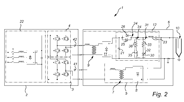
Fig. 2 illustrates a schematic circuit representation of a high-voltage
power supply system for powering an electrostatic precipitator in accordance
with an embodiment of the present invention;
Fig. 3A illustrates a schematic waveform representing the voltage
across a storage capacitor of a pulse forming circuit during an oscillation
cycle in accordance with an embodiment of the present invention;
Fig. 3B illustrates a schematic waveform representing the current in a
pulse supply circuit and into the ESP during an oscillation cycle in
accordance
with an embodiment of the present invention;
Fig. 3C illustrates a schematic waveform representing the voltage
across an ESP connected to a high voltage power supply system during an
oscillation cycle in accordance with an embodiment of the present invention.
Fig. 4 is a schematic block diagram of an alternative embodiment of
the pulse supply circuit in figure 2.
CA 03078269 2020-04-02
WO 2019/072786
PCT/EP2018/077380
9
DETAILED DESCRIPTION
In the following detailed description, preferred embodiments of the
present invention will be described. However, it is to be understood that
features of the different embodiments are exchangeable between the
embodiments and may be combined in different ways, unless anything else is
specifically indicated. Even though in the following description, numerous
specific details are set forth to provide a more thorough understanding of the
present invention, it will be apparent to one skilled in the art that the
present
invention may be practiced without these specific details. In other instances,
well known constructions or functions are not described in detail, so as not
to
obscure the present invention.
Fig. 1 is a schematic block diagram of a high-voltage (pulsed) power
supply system 1, particularly suitable for powering an electrostatic
precipitator
(ESP) 10. The system 1 can be divided into two parts, a pulse unit tank 5, 6
and a control cabinet 2 where the control cabinet can be understood as a
controllable AC supply circuit configured to generate a supply voltage to the
pulse unit tank which in turn transforms this supply voltage to a suitable
level
in order to power the ESP 10. More specifically, the pulse unit tank comprises
a high-voltage pulse supply circuit 6 and a high-voltage DC supply circuit 5
whereby the pulse unit tank is arranged to supply a high DC base voltage
(e.g. magnitude in the range of 20 kV to 150 kV) with superimposed high-
voltage micro pulses (magnitude in the range of e.g. 40 kV to 120 kV) at a
rate of 2 to 200 pulses/s, preferably 100 pulses/s. Generally, the voltage
applied to the discharge electrode (of the ESP) is of a negative polarity,
wherefore the preceding voltage ranges may be understood as ranging from -
20kV to -150kV for the DC base voltage and from -40kV to -120kV for the
micro pulses.
The AC supply circuit 2 is configured to generate a first AC supply
voltage and a second AC supply voltage for the DC supply circuit 5 and the
pulse supply circuit 6 respectively. The frequency AC supply voltages is
within
the medium frequency range, i.e. between 100 Hz and 5000 Hz, preferably in
the range of 200 Hz and 2000 Hz. By using this arrangement (medium
CA 03078269 2020-04-02
WO 2019/072786 PCT/EP2018/077380
frequency supply together with a high-voltage switching circuit) advantages in
terms of low losses, reduced tank size and weight, reduced manufacturing
costs, etc. may be achieved. Moreover, the AC supply circuit 2, and more
specifically the semiconductor switches (e.g. IGBTs) of the AC supply circuit,
5 which are configured to control the output voltage frequency, can be
positioned within a control cabinet in a protected environment, as opposed to
prior known systems using an AC feed utilizing higher frequencies which must
be placed closed to the transformer(s) which is/are arranged outdoors in
relatively harsh environments.
10 Fig. 2 is a schematic circuit representation of a high-voltage
power
supply system 1 in accordance with an exemplary embodiment of the present
invention. In reference to this drawing, further details of the system's 1 sub
units and their functional aspects will be described. The high-voltage power
supply system 1 comprises an AC supply circuit 2 which is configured to
generate a first AC supply voltage and a second AC supply voltage. In more
detail, the AC supply circuit 2 includes a first power inverter 3 and a second
power inverter 4 configured to convert a DC feed voltage to the first and
second AC supply voltages respectively. The DC feed voltage is generated by
means of DC supply circuit 22 comprising a three-phase rectifier bridge
connected to AC mains (e.g. 380V/50Hz). Naturally, there are other ways to
provide a suitable DC feed voltage to the power inverters 3, 4 that are within
the skilled artisan's general knowledge (e.g. using a single phase supply
instead of a three phase, connecting the inverters directly to a DC source,
etc.) and will therefore for the sake of brevity be omitted.
Each of the power inverters 3, 4 comprises a set of IGBTs with an anti-
parallel diode connected across each transistor, arranged in a full bridge
configuration. However, other topologies commonly used in high power
applications are feasible, such as e.g. half bridge inverters. Even though
IGBTs are shown in the illustrated example, other semiconductors switches
are applicable such as e.g. MOSFETs, BJTs, etc.
Further, the high-voltage power supply system 1 has a DC supply
circuit 5 connected to the output of the first power inverter 3. The DC supply
circuit 5 includes a first transformer 7 and a first rectifier circuit 8 for
CA 03078269 2020-04-02
WO 2019/072786 PCT/EP2018/077380
11
transforming and converting the first AC supply voltage to a DC base voltage
(magnitude in the range of 20 kV to 150 kV) for the ESP 10. The negative
electrode (i.e. having a negative potential UB) of the first rectifier circuit
8 is
connected to the discharge/emitter electrode of the ESP, while the positive
electrode is grounded.
Moreover, a pulse supply circuit 6 is connected between the output of
the second power inverter 4 and the ESP 10, where the pulse supply circuit
has a second transformer 9 and a second rectifier circuit 11 for transforming
and converting the second AC supply voltage to a DC pulse supply voltage
(magnitude is e.g. in the range of 40kV to 120kV). The positive terminal of
the
second rectifier circuit 12 is grounded while the negative terminal (having a
negative potential 1.1c) of the second rectifier circuit 11 is connected to
the
discharge/emitter electrode of the ESP 10 via a number of components 23,
24, 27 included in the pulse forming circuit 12. The pulse forming circuit 12
is
then configured to generate high-voltage pulses for the ESP 10 (the pulses
are accordingly superimposed on the DC base voltage UB).
Still further, the system 1 comprises a pair of optional series capacitors
41, 42, namely a first series capacitor 41 connected between the first power
inverter 3 and the first transformer 7 of the DC supply circuit 5, and a
second
series capacitor connected between the second power inverter 3 and the
second transformer 9 of the pulse supply circuit 6. The series capacitors 41,
42 form a series resonant circuit together with the leakage inductance of the
transformers 7, 9 and any potential primary chokes, why the IGBTs can be
controlled so that they turn off at lower current magnitudes thereby reducing
power losses and increasing the lifespan of the IGBTs. Moreover, output
ripple can be reduced by employing the series capacitors 41, 42.
Moving on, the pulse supply circuit 6 comprises a pulse forming circuit
12, connected between the second rectifier circuit 11 and the ESP 10. The
pulse forming circuit is configured to generate and forward high-voltage
pulses to the ESP 10. The pulse forming circuit may be configured such that
the pulse repetition frequency in the range of 2-200 Hz, each pulse for
example having a pulse width in the range of 50 to 150 ps. The pulse
repetition frequency is suitably controlled by means of a control circuit or
CA 03078269 2020-04-02
WO 2019/072786
PCT/EP2018/077380
12
ignition circuit connected to the switching element(s) of the high voltage
switching circuit 24, however this will be discussed in more detail in the
following.
The pulse forming circuit 12 has a storage capacitor 21 connected in
parallel with the second rectifier circuit 11, i.e. between the negative
(output)
terminal and the positive terminal of the second rectifier circuit 11, or
between
the negative terminal of the second rectifier circuit and ground. Thus, the
voltage across the storage capacitor 21 is charged to the same level as the
DC output of the second rectifier circuit 11, in this case, Uc. Connected in
series between the negative terminal of the storage capacitor 21 and the ESP
10 is a first series inductance 23 and a high voltage switching circuit 24.
The
high voltage switching circuit 24 comprises an anti-parallel coupling of a
thyristor 25 or a thyristor chain and a diode 26 or diode chain. In other
words,
the thyristor(s) and the diode(s) is/are connected in mutually oppositely
conducting directions in order to enable the diode or diodes to have a
blocking effect on current heading towards the second rectifier circuit 11
when
the thyristor(s) is/are off. Component chains are used in order to be able to
handle the high voltages in the circuit without burning or destroying the
components.
A control circuit or firing circuit (not shown) is used to fire the
thyristor(s) at a predefined frequency in order to monotonously form a series
resonant circuit causing a sudden increase in voltage, VESP, across the ESP,
(i.e. the negative potential of the discharge electrode is increased) and a
corresponding decrease in voltage, Vc, across the storage capacitor 21. This
is schematically illustrated in the waveforms shown in Fig. 3A and 3C, where
Fig. 3A shows the voltage across the storage capacitor 21 over time, and
more specifically during an oscillation cycle, and Fig. 3C shows the voltage
across the ESP 10 during an oscillation cycle. Moreover, Fig. 3B illustrates
the current flowing through the pulse forming circuit 12 and into the ESP 10
during an oscillation cycle.
Reverting back to Fig. 2, the pulse forming circuit 12 also has a
coupling capacitor 27 connected in series between the first series inductance
23 and the discharge electrode of the ESP 10. The coupling capacitor 27 aids
CA 03078269 2020-04-02
WO 2019/072786 PCT/EP2018/077380
13
to forward and add the pulse voltage on top of the DC base voltage and also
to mitigate the risk of short circuiting the DC supply 5 by means of the pulse
supply 6.
Further, the pulse forming circuit 12 includes an optional auxiliary
circuit 30 connected in parallel with the high voltage switching circuit 24
and
the storage capacitor 21. Stated differently, the auxiliary circuit 30 has one
terminal connected between the high voltage switching circuit 24 and the first
series inductance 23 and the other terminal connected to ground. The
auxiliary circuit 30 here has two parallel branches 31, 34, where each branch
has one terminal connected to a node between the high voltage switching
circuit 24 and the first series inductance 23 and the other terminal connected
to ground. One of the branches is denoted as a protective branch 31 which
includes a first series resistance 33 and a series diode 32 for limiting
voltage
peaks across the high voltage switching circuit 24. The auxiliary circuit 30
further has an optional restoring branch 34 including a second series
resistance 36 and a second series inductance 35 in order to restore a charge
of the coupling capacitor 27 between pulses. Preferably, the second series
inductance has a relatively high inductance value, e.g. in the range of 0.1H
to
10H, such as e.g. 1H.
It is noted that other examples of auxiliary circuits 30 are possible. In
particular, the auxiliary circuit may be simplified, and include e.g. only a
restoring branch, which may include only an inductance or only a resistor.
Figure 4 shows an alternative embodiment of the pulse forming circuit
12'. The components are substantially the same as in the circuit 12 in figure
2, with some differences.
The rectifier 11 is here connected to provide a positive supply voltage.
Further, the storage capacitor 21' and the high voltage switching circuit 24'
have changed position, such that the switching circuit 24 is connected in
parallel with the rectifier 11, i.e. between the rectified outputs. With this
solution, an additional impedance 28, here an inductance in series with a
resistance, is required between the rectifier output and the storage capacitor
21'.
CA 03078269 2020-04-02
WO 2019/072786 PCT/EP2018/077380
14
The protective branch 31 and the restoring branch 34 maybe
connected in the same way as in figure 2, i.e. in parallel with the storage
capacitor 21' and switching circuit 24'.
Even though the invention has been described with reference to
specific exemplifying embodiments thereof, many different alterations,
modifications and the like will become apparent for those skilled in the art.
For
example, each of the power inverters 3, 4 may have their own separate feeds
with a rectifier circuit and DC-link capacitor. The DC feed circuit 22 may for
example be supplied by a single phase AC instead of a three-phase AC. Such
and other obvious variations to the disclosed embodiments can be
understood and effected by the skilled addressee in practicing the claimed
invention, from a study of the drawings, the disclosure, and the appended
claims. Furthermore, in the claims, the word "comprising" does not exclude
other elements or steps, and the indefinite article "a" or "an" does not
exclude
a plurality.