Note: Descriptions are shown in the official language in which they were submitted.
1
Metrology device, system and method
Field of the invention
The invention relates to metrology or testing methods and devices for
characterizing a temperature-dependent process performed on a surface or
substrate.
Background of the invention
Metrology techniques may be used to characterize processes in which the
temperature of a substrate affects one or more parameters of a treatment
process of the
substrate. The examples given in this description relate to semiconductor or
metallurgical
fabrication processes performed on a substrate such as a silicon wafer.
However, other
processing techniques in other contexts may likewise require a substrate or
surface to be
at a particular temperature during processing. Such processing techniques may
include
coating, deposition, etching, abrasion, washing, annealing, sintering,
polishing or other
processes which are affected by the substrate temperature. Metrology
techniques can be
used to obtain characterization information which can be used to calibrate or
adjust
process parameters to obtain the desired process result on the substrate, in
dependence
on the substrate temperature. For example, it may be desired to identify an
optimum
temperature for depositing a particular characteristic (eg thickness or
crystallographic
structure) of a particular material deposited on a particular substrate, or to
determine the
characteristic(s) of the deposited material at each of various substrate
temperatures.
Prior art
It is known to characterize a temperature-dependent silicon fabrication
process
by performing the process on one or more test wafers, with the test wafers at
a different
temperature for each test. The characterization may be performed with one test
wafer,
heated to a first temperature, then a second, then a third, etc, and with
different regions of
the wafer exposed to the fab process for each test. Or different wafers may be
used for
each test. In order to achieve a useful characterization of the process
variation with
temperature, many tests are needed, and many wafers, and the testing process
takes a
great deal of time. A fine-grained characterization would be out of the
question.
Date Recue/Date Received 2020-04-24
2
By way of example, it is known in some thin-film fabrication methods to
elevate
the substrate (target) temperature in order to obtain a particular desired
deposition rate
and/or crystallographic structure of the deposited elements. Likewise, the
substrate
temperature may be varied to obtain a desired etch rate of a particular
etching process,
for example. In the growth of Neodymium Iron Boron (NeFeB) magnetic films, for
example, the material may be deposited using sputtering with the substrate at
a
temperature (TD) in the range 20 C to 500 C
(https://doi.org/10.1063/1.2710771). Post
deposition annealing up to 750 C for multiple minutes enables crystallization
and
promotes grain growth. This annealing step is not only sensitive to the
annealing
temperature (TA) and annealing time (tA), but also the temperature ramp rate
during
heating (dT/dtA ) and cooling (dT/dtA_). This simple example includes five
temperature-
related parameters. If one were to scan the parameter space with just 4 values
of each
parameter, there would be 45= 1024 possible combinations. In practice,
processes are
characterized for a much smaller number of combinations on grounds of time and
cost.
Brief description of the invention
The present invention aims to overcome at least some of the disadvantages of
the prior art. To this end, a metrology device according to the invention is
described in
claim 1, a metrology array according to the invention is described in claim 6
and
characterization methods according to the invention are described in claims 9
and 10.
Detailed description of the invention
The invention will now be described in detail with reference to the attached
drawings, in which:
Figures 1A and 1B show plan and cross-sectional view of a MEMS hotplate
element 1 suitable for carrying out the invention, including a central plate
4, tethers 6 and
electrical leads 10, 12 which may be part-metallized 14. An electrode beneath
the plate
may be used for resonant actuation and detection.
Figure 1C depicts a 3x3 array 2 of MEMS elements 1 such as those of figure 1.
Figures 2A and 2B illustrate two variants of a shielded array 20. The shield
22
covers the electrical leads 10,12,14 as well as the heating elements of the
device 1, but
leaves the hot plate exposed.
Date Recue/Date Received 2020-04-24
3
Figure 3A illustrates the die 104 containing the MEMS hotplate array 2
packaged
in a ceramic chip holder 102. A lid 110 with opening 112 shield the electrical
connections
106.
Figure 3B is a side view of the ceramic chip 102 mounted in a socket. In this
implementation the lid is mounted on the socket.
Figure 4 is an example of the fabrication and analysis platform 100 with the
socket, along with a temperature sensing element 118 and multiplexer 120
mounted on a
PCB 102.
Figure 5 is an example of a cold wall CVD system 150, the fabrication and
.. analysis platform 100 and a thermal control unit 200.
Figure 6 is an example of a magnetron sputtering system 160 with the
fabrication
and analysis platform 100 and a temperature control unit 200a and a frequency
control
unit 200b which interface with a computer 202.
Figure 7 is an example of the flow in information for sensing and controlling
the
temperatures of the MEMS hot plates used for magnetron sputtering deposition.
Figure 8 is an example of a reactive ion etching unit 170 and a fabrication
and
analysis platform 100 along with a thermal control unit 200.
Figure 9 is an example of a vacuum annealing chamber in a homogeneous
magnetic field 300. A MEMS hot plate element is electrostatically actuated in
a torsion
mode which is sensed by a lock in amplifier 200c. Thermal treatment is
controlled by a
thermal control unit 200a.
Figure 10 is an example of a vacuum annealing chamber in an inhomogeneous
magnetic field. The MEMS hotplate is actuated in a vertical translation mode
by a
piezoelectric shaker 408 and sensed using a Doppler vibrometer measurement
system
consisting of the laser and optics 406 and control unit 200d. Thermal
treatment is
controlled using the thermal control unit 200a.
It should be noted that the figures are provided merely as an aid to
understanding
the principles underlying the invention, and should not be taken as limiting
the scope of
protection sought. Where the same reference numbers are used in different
figures, these
are intended to indicate similar or equivalent features. It should not be
assumed, however,
Date Recue/Date Received 2020-04-24
4
that the use of different reference numbers is intended to indicate any
particular degree of
difference between the features to which they refer.
This invention proposes to use arrays of MEMS hot plates as deposition
substrates (targets). Such an array may consist of individual elements, arrays
of 2x2
elements or 10x10 or more. As each element can be set to a well-defined
temperature a
total of 100 deposition temperatures could be tested simultaneously. Post
deposition
etching or thermal treatments could again be performed simultaneously and
individualized
for each plate. Consequently, finding the optimal thermal conditions for
deposition,
annealing, end etching could be accomplished 100x faster. The method described
is
applicable for deposition, annealing, and etching processes which occur at
vacuum, at
pressures typically, but not limited to, below 2x10⁻² mbar. Such deposition
methods may
include, but are not limited to, Low pressure Cold Wall Chemical Vapor
Deposition (CVD),
Plasma Enhanced CVD, Sputtering, Reactive Ion Sputtering, Magnetron
Sputtering,
Atomic Layer Deposition (ALD), and Physical Vapor Deposition (PVD) (including
thermal
and e-beam evaporation). The etching may take place in a reactive ion etching
system,
where an RF voltage creates a plasma which results in an an-isotropic etch of
the
substrate. Annealing may occur in vacuum or rarified gas (low pressure). As
often
processes are temperature dependent, the MEMS hotplate elements enable the
efficient
optimization of deposition, etching and annealing parameters.
In the context of semiconductor fabrication, the invention may MEMS hot plates
as a tool for thin-film deposition, reactive etching, and thermal treatment
methods. The
MEMS hot plates enable high level of control of the temperature of the
deposition
substrate, deposition mass and post deposition thermal treatment. Lastly, the
MEMS can
also enable intrinsic characterization of the deposited thin-film. The ability
to create an
array of MEMS hotplate elements allows the user scan the thermal landscape
with high
precision. The ability to test deposition, etching, and post deposition
thermal treatment
parameters in parallel, along with in-situ feedback, improves the efficiency
in optimizing
thin-film growth protocols.
The heating elements create an array of deposition targets.
Each target can be held at a unique, well defined temperature during
deposition
(TD) or etching (TE).
The temperature can be monitored using the resistance of the heating elements
Date Recue/Date Received 2020-04-24
5
The temperate can be changed (dT/dt+) in millisecond time scales (tramp)
(which is
interesting for multi-layer depositions were each layer can be deposited at a
unique
substrate temperature).
By adding an electrode below the heating elements, the elements can be
resonated. The change in resonance frequency (fp) is a direct measure of the
mass of the
deposited material. (The deposition rate may be temperature dependent).
After deposition, the heating elements can be used as annealing elements. In
this
case the temperature (TA), temperate ramp rates (dT/dtA) and annealing
temperature time
(tA) can be set individually for each heating element.
The resonance can be used to monitor the annealing effects. For example: if a
magnet is being annealed then and external homogeneous field will induce a
torque on
the magnets. This restoring torque will result in a frequency change of a
torsion mode.
Therefore, the frequency shift in the torsion mode due to an applied external
field can be
used as a measure of the magnetization of the deposited film.
The modular system would also allow the chip containing the thermal array to
be
mounted in a specially developed socked in characterization systems. This
includes, but is
not limited to, material characterization systems such as optical microscopy
(with vacuum
chambers), Scanning Electron Microscopes (SEM), Vacuum Atomic Force
Microscopes
(AFM), Vacuum X-ray diffractometers (XRD), and Raman Spectrometers, etc. The
array
enables the characterization of materials deposited on the hotplates over a
wide thermal
parameter space, with respects to surface morphology, crystallography, and
chemical
bond vibrations which may alter as a function of temperature or during thermal
annealing
processes.
A small die, such as 2.5 x 2.5 mm2 may contain, for example, an individual hot
plate with a diameter or up to 1 x 1 mm2, or for example, an array of 2 x 2
hot palate with a
diameter of 0.5 mm each or for example, an array of 3 x 3 with a diameter of
0.2 mm
each, etc. up to an array, for example of 10x10 with a diameter of 0.05 mm
each.
To summarize: These arrays can be used to optimize growth, post growth
annealing conditions and etching, in particular related to thermal treatment.
Implemented
as resonators they can be used for real-time feedback of deposition rates,
etch rates, and
serve to track and quantify changes in material properties due to annealing
treatments.
Date Recue/Date Received 2020-04-24
6
The device described may advantageously be made of a single material. One
could also add a stack or a conformal coating to ensure chemical
compatibility. For
example, it is known that a conformal ALD deposited layer of A1203 will
chemically
separate incompatible materials such as silicon and gold, at elevated
temperatures.
The MEMS hotplate device 1 depicted in figure 1 A and B includes a central
plate
element 4 which is mechanically suspended by heating elements 6. The heating
elements
6 a conducting and by applying a voltage across them a current will be induced
which will
heat the central plate. The number of heating elements must be even, and is
typically 4,
but often 6 or 8. There can also be only two heater elements, or as many as 16
or even
32.
The central plate can be heated using the heating elements to 500 deg C or
over
1000 deg C or over 2000 deg C up to 4000 deg C if the heating elements and the
central
plate are made of refractory ceramic materials such as, but not limited to
HfC, TaC, or
TaHfC. The heating elements suspend the central plate element above the
substrate
such that it is not touching the substrate. The void between the plate and the
substrate is
typically 2- 20 microns deep, but may be larger. The heating elements are such
that they
can expand, flex and bend as they are heated. This flexure releases the
thermal stresses
that occur as the heating elements and the central plate are heated to high
temperatures.
The structures are made of a single material. The material is curved to the
substrate at the
anchors. This has two functions; 1 it physically attaches the heaters to the
substrate and 2
it creates an overhand so that deposited material does not short out the
devices. This is
depicted in the inset of figure 1B
The central plate element is typically 50-100 microns in diameter, but
depending
on the application smaller diameters, down to 10 microns or smaller can are
interesting
when larger arrays are desired (described below), or the thermal time
constants are
needed to be very small, such as well below 1 millisecond. Correspondingly,
much larger
central plate elements may be of interested, 200 microns, or even 400 microns
or even
600 microns in diameter. The MEMS hotplate devices with larger diameter
central plates
will tend to have larger number of heating elements, they will have a slower
thermal
response time which defines the time needed to heat or cool the MEMS hotplate
devices,
and will typically not be able to heat to as high a temperature due to the
thermal radiation
cooling effects. For these reasons the larger plates will have a maximum
temperature in
the range of 1000 K or up to 2000 K depending on geometry, material and number
of
Date Recue/Date Received 2020-04-24
7
heating elements. To minimize this cooling effect, materials with low emission
coefficient
are best suited for larger MEMS hotplate device with larger plates.
The hotplate device includes electrical leads, 10 one of which may be ground
12.
To improve the efficiency these leads can be metallized 14, which reduced the
electrical
resistance in the leads. Typical resistance of each heating element is 1000
Ohms, but can
be lower or higher. Typical resistance of the metallized leads is below 1 Ohm.
Beneath
the central plate 4 and the heating elements 6 there is a void. Beneath the
void there is an
electrode 16, which may be segmented. This electrode make is possible to
mechanically
actuate and/or sense the corresponding displacement of the central plate 4.
Such sensing
can be capacitive sensing, or optical sensing or piezoresistive sensing. The
actuation can
be thermal, capacitive (electrostatic) or piezo-electric using a shaker
platform. Such
actuation is typically alternating, resulting a vibrational motion of the
pate. Ideally this is on
resonance or close to resonance. For the devices presented the resonant
frequency is
typically between 10 kHz and 1 MHz. For larger plates this can be as low as
100 Hz, or for
smaller plates this can be as high as 10 MHz or even 100 MHz. Depending on the
actuation method the resonant mode can be out of plane, in plane or a
torsional mode.
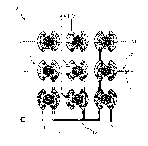
The MEMS hotplate device 1 can be placed in an array as illustrated in Figure
1C. Figure 1C shows an example of an array 20 of 3x3 hot plate devices. Each
device can
be individually addressed. In the example given the devices have 6 heater
elements each.
In the example given there the array is a 3x3 array of MEMS hotplate device.
One could
also conceive a smaller array of 1x1 or 2x2 MEMS hotplate elements,
alternatively a
significantly larger array can also be constructed, of 4x4, 5x5 etc. even up
to 10x10
elements. These arrays built on dies 2.5 x 2,5 mm2, but smaller or larger dies
can be
considered typically ranging from 1x1 mm2 to 10 x 10 mm2 or larger. In Figure
1C the
elements of the array are innumerate in roman numerals, in this example from
Ito IX to
uniquely identify the nine electrical leads needed to heat the plates to nine
unique
temperatures.
The MEMS hotplate devices 1 are used to heat the central plate 4. The heat is
applied by passing a current though the heater devices 6. The current is
driven by
applying a voltage bias, typically between 0-5 volts between the leads 10 and
12. These
leads are metallized 14 to reduce electrical losses between the power source
and the
heating elements. The voltage bias drives a current thought the device,
proportional to
the device resistance. The resistance is typically a function of temperature
and may be
linear or not. The hotplates are calibrated and a look-up table can be used to
determine
Date Recue/Date Received 2020-04-24
8
their temperature by comparing the hot pate element electrical resistance
change with
respect to a reference temperature. For materials such as metal, or highly
doped
semiconductors, as is the case with highly doped silicon with phosphor, the
resistance
increases with temperature. This temperature dependence means that monitoring
the
resistance, for example by measuring the current resulting from the applied
voltage bias,
can be used to determine the temperature of the hotplate of a calibrated
device. The
increasing resistance with rising temperature also helps stabilize the MEMS
hotplate
device as the heating becomes self-limiting. (If the heating elements are made
of a
material with a decreasing resistance with increasing temperature then it is
preferred to
apply a current bias instead of a voltage bias.) The voltage bias can be
constant, ramped
or modulated. A square wave, or individual square pulse can be applied. By
monitoring the
resulting current one can calculate the thermal time constant TT. For known
material
properties and MEMS hotplate device geometries one can use this to calculate
the
thermal load. If the thermal properties are known and the thermal load is
measured then
this information can be used to determine the mass of the material deposited
or etched
from the central hotplate. Hence, the thermal control and feedback module can
used to 1)
set a target temperature, b) set a thermal annealing profile and c) used to
measure
thermal time constants from which material properties and/or deposition and
etch rates
can be deduced. As outlined in the next paragraph the thermal control and
feedback
module can also d) measure piezoresistive changes of the resistance of the
heating
elements and e) thermo-mechanically actuate the device.
The MEMS hotplate devices include an electrode 16 placed below the central
plate. This electrode can be used to capacitively sense the distance between
the central
plate and the electrode. Applying a voltage to electrode 16 will result in the
electrostatic
attraction of the plate. Resonant or pulsed signals can be used to actuate
mechanical
modes in the MEMS hotplate device. These modes can be sensed using the same
capacitive electrode, optically, by reflecting a laser off the surface of the
central hotplate,
and/or piezoresistivity, by measuring changes in the resistance of the heating
arms, which
are also the flexural elements of said resonator. Changes in the resonance
frequency, f, of
the modes (at a fixed temperature) can be used to measure changes in mass, m:
Af Am
f m
The changes in mass, measured though changes in the thermal response time or
preferably by changes in resonance frequency (equivalent to the mechanical
response
time) can be used to determine deposition or etch rates, an important feedback
feature
Date Recue/Date Received 2020-04-24
9
enabled by the MEMS hotplate devices. Of both mechanical and thermal
timescales are
precisely measured, then this information can be used to calculate both the
mass
(mechanical mass) and the thermal load (thermal mass) of the deposited
material. Like
this it is possible to determine a deposition rate or etch rate for each
element of the MEMS
hotplate device array independently and in-situ of the thin film deposition or
etching
system.
To protect the electrical leads from the deposition material, or the reactive
ion
etching, they may be covered. Such masking is illustrated in figure 2A and 2B.
In one
implementation (Figure 2A) a masking plate 22 is mounted on spacers 24 that
raise the
masking plate above the MEMS hotplate device array. In Figure 2B the masking
plate 22
is grown on a planarized spacer 24. The material of the masking plate is
chosen so that it
does not interfere with the thin-film growth process or is not significantly
etched by the
reactive ion etching process. This may be, but is not limited to a hard metal
such as
tungsten or Iron, or alternatively silicon, or silicon carbide, or a ceramic
material. The
spacer may be made of an easily etched material such as silicon dioxide, or a
polymer
such as 5U8, such that the etch process during fabrication fully releases the
MEMS
hotplate device, resulting in a suspended, free standing structure with an
appropriate
undercut.
Depending on the deposition and etch processes performed, it may also be
possible to only mask the heater elements 6, as is illustrated in figure 1B
and in the
example given in the prior art. Here, the electrical readout leads are curved
up at the
edges, illustrated in figure 1B. This prevents an an-isotropically deposited
conductor from
shorting out the structures. For the deposition of very thin, insulating
materials, no such
shielding is required. An example, but not limited to, is the atomic layer
deposition of
A1203.
The MEMS hotplate device array is built on a chip, typically 1x1-10x10 mm2.
This
chip 104 is mounded in a chip holder, typically a ceramic chip holder 102 as
illustrated in
figure 3A (perspective view) and figure 3B cross sectional view. Electrical
contacts are
made from the leads, 10 and 12 to the chip holder pads 108 with wire bonds or
ball bonds
106, typically made of aluminum or gold. A shield 110 with opening 112 is
mounted over
the die and electrical connectors on spacers 114. This shield protects the die
and
electrical leads from coating by the deposition materials or the reactive ion
etching. In
figure 3B illustrates the chip holder 102 mounted in a socket 116. In this
implementation
the socket includes the spacer 114 and shield 110 with the opening 112 which
exposes
Date Recue/Date Received 2020-04-24
10
the MEMS hotplate devices to the flux of deposition material or the reactive
ions. The
contacts 106 of the chip holder interface with contacts on the socket.
Figure 4 illustrates the integration of the socket 116 which includes the chip
holder 102 and mounted die 104, together with a thermometer 118 and
multiplexer 120 on
a disc, such as a PCB 101. This fabrication and analysis platform 100 replaces
the wafer
which would typically be used in such deposition and etching processes. The
electrical
control signals, for sensing and actuation of the MEMS heater devices, are
transmitted to
and from the fabrication and analysis platform through electrical wires 122.
In an
alternative implementation these wires could be replaced by wireless
communication
protocols such as Bluetooth. While in this example the PCB 101 includes
thermometry
feedback 118 and a multiplexer 120, other implementations may include
additional control
and logic elements, including, but not limited to, hall sensors for magnetic
field sensing,
integrated PID loops for temperature control of the MEMS hotplate devices and
phase
locked loop (PLL) circuits for monitoring changes in the resonance frequency
of the
MEMS hotplate devices. In its simplest implementation the fabrication and
analysis
platform 100 only includes interfacing with the communication and control
wires 122.
While the hotplate devices may each independently be set to an individual
temperature,
the temperature measured by the thermometer 118 defines the base temperature
(or
minimum temperature) and is also used for calibration of the MEMS hotplate
devices.
Figures 5, 6, and 7 exemplify deposition systems in conjunction with the MEMS
hotplate devices along with a schematic illustration of the communication and
control
(Figure 7). The examples provided include Cold Wall CVD and Magnetron
sputtering thin-
film deposition systems.
Figure 5 illustrates a Cold Wall Low Pressure Chemical Vapor Deposition
(CWLPCVD) system 150, characterized by a gas manifold system 152 which feeds
the
precursor and carrier gases into the vacuum chamber 140 through a gas vacuum
feedthrough 154. The gas mixture is released into the vacuum chamber through
the cold
showerhead 158. The gas is directed towards the fabrication and analysis
platform with
the array of MEMS hotplate devices which is mounted on a platform 156. The gas
mixture
reaching the hot central hotplate of the MEMS hotplate devices will react and
deposit the
desired material on the central hotplate. Surplus gas is evacuated from the
vacuum
chamber through the vacuum pump port 144. The vacuum is monitored by the
pressure
sensor 142. In order for the of MEMS hotplate devices to function as designed
the
pressure in the vacuum chamber must be low, below 104 mbar for temperatures up
to 300
Date Recue/Date Received 2020-04-24
11
deg C, below 10' mbar for temperatures up to 800 deg C and ideally below 10-3
mbar for
temperature exceeding 800 deg C. MEMS hotplate materials and specific
geometries and
heater element configurations will influence such parameters. For example,
smaller
central hotplates 4, with a diameter for example of less than 50 microns,
coupled to a
larger number of heating elements 6, can sustain higher temperatures at higher
pressures. For temperatures above 1000 deg C thermal radiation becomes a
significant or
even dominant cooling mechanism which in turns limits the size of the hotplate
and
imposes additional constraints on the number of heating elements needed to
obtain a
desired setpoint temperature even as the vacuum pressure drops well below 10
mbar.
In the CWLPCVD realization the fabrication and analysis platform includes a
thermometer 118 for temperature monitoring and calibration but no multiplexing
element.
In this case each element is addressed directly using the commination
electrodes 122b
which are fed out of the vacuum chamber through electrical vacuum feedthrough
port 148
to a control and communication module 200. This module may be stand alone or
interface
with a computer, tablet or smart phone, for example using a USB connection or
wireless
communication protocols.
The second example, illustrated in figure 6, is that of a magnetron sputtering
system 160. The system includes a vacuum chamber 140, vacuum pumping port 144
and
vacuum gauge 142 as well as a blanking shutter 147 and gas inlet port 146. The
blanking
shutter prevents deposition on the fabrication and analysis platform until a
predetermined
time, such as when all set temperatures of the MEMS heater devices have
reached their
desired setpoint. The gas inlet port can be used to feed inter gasses such as
argon into
the chamber, needed for sputtering, as well as chemically active gasses such
as, but not
limited to, hydrogen, nitrogen or oxygen for reactive sputtering. The
magnetron sputtering
system also includes cathode targets 162a-c which may be DC or AC targets
depending
on the desired deposition materials. Typically, SC cathodes are uses for
conductors such
as metals, and AC cathodes for insulators and semiconductors such as 5i02 and
Si.
Reactive sputtering modes can be used for the deposition of Oxides, Nitrides
and
Carbides. The anode is formed by the platform 156 and on the fabrication and
analysis
platform 100. The same pressure-temperature considerations as discussed for
the
CWLPCVD implementation also apply for the magnetron sputtering system, as well
as the
other deposition and reactive ion etching, and thermal annealing and
characterization
systems.
Date Recue/Date Received 2020-04-24
12
In this example of the implementation the on the fabrication and analysis
platform
includes a multiplexing element 120 which can address a large array and
transfer signals
between the fabrication and analysis platform (such as temperature
information) and the
MEMS heating devices (such as the set voltage and measured device resistance)
and the
.. control and communication modules 200a and 200b. In this example the wire
bundle 122
and feedthrough 148 may contain fewer cables as the information is digital,
compared to
the direct electrical access to the devices described previously. There are
two
independent control and communication modules. Control and communication
module
200a is used to set and monitor the temperature profile of the MEMS hotplate
device
array, were the control and communication module 200b is used for monitoring
the
resonance frequency, of the mechanical displacement of the MEMS hotplate
device array.
As discussed above, this information can be used to determine deposition rates
and
additional material properties. In either case the modules can be stand alone
or interface
with a computer 202, tablet or cell phone using USB or Bluetooth
communication.
Figure 7 illustrates the flow of information. This example is specific to the
magnetron sputtering setup which generates a flux of deposition material IF,
but is
equivalent to the other deposition, etching or annealing and characterization
systems. A
computer 202 is used to set a temperature profile and sense the mechanical
displacement
of a MEMS hotplate device array. The information (temperature control Tcont
and
frequency control fcont) is sent to the corresponding communication and
control modules
200a and 200b. These modules interpret the commands and relay the information
into the
vacuum chamber of the deposition system (TData and fData) to the multiplexer
120 on the
fabrication and analysis platform 100. The multiplexer addresses directly the
array and
applied the drive signals Min and records the output signals Mout from the
MEMS hotplate
device array. The multiplexer also interfaces with additional sensors on the
fabrication and
analysis platform such as the temperature sensor 118 used for calibration. The
recorded
information is sent back to the computer via the temperature communication and
control
module 200a and the control unit and the resonance communication and control
module
200b. The communication and control module can set the desired temperature
profile of
the MEMS hotplate device array and interpret measurements, such as changes in
resonance frequency or thermal timescales as described above. Consequently,
both etch
rates and material properties can be deduced from the measurements performed
by the
communication and control units during the deposition process.
The provided thin-film deposition examples are illustrative and not limiting.
Using
the same methodology, the system described can also be included in other,
standardized
Date Recue/Date Received 2020-04-24
13
thin-film deposition systems, such as, but not limited to, Physical Vapor
Deposition System
(in which case the fabrication and analysis platform 100 is inverted, facing
down, as the
material flux would typically come from below), Atomic Layer Deposition,
Sputtering, and
Reactive Ion Sputtering.
Thin-film etching can be performed by reactive ion etching (RIE). Such a setup
is
illustrated in figure 8. The RIE system 170 includes a vacuum chamber 140
consisting of a
vacuum gauge 142 and pumping port 144 as well as a gas vacuum feedthrough line
154
interfacing with a gas flow manifold. Such a system enables the flow of
reactive and inert
gases such as, but not limited to 02, NO, N20, Ar, H2, HBr, SF6, CF4, NF3,
CHF3, C4F8, C12,
.. BCI3, CCI4, NH3. The gas forms a plasma between the electrodes formed by
the chamber
walls and gas inlet 176, held a ground) and the target which consists of the
platform 156
and the fabrication and analysis platform 100 set to an oscillating potential
at radio
frequencies, typically at 13.56 MHz. The temperature of the etch is set by the
array of
MEMS hotplate devices through the communication and control module 200. In
this
example no multiplexing is implemented and the communication and control
module 200
interfaces directly with the MEMS hotplate device array. The communication and
control
module can set the desired temperature profile of the MEMS hotplate device
array and
interpret measurements, such as changes in resonance frequency or thermal
timescales
as described above. Consequently, both etch rates and material properties can
be
deduced from the measurements performed by the communication and control units
during the etching process. The reduced mass will also result in a reduced
thermal load,
hence the etch rate could also be monitored by measuring the thermal time
constant of
the devices. In such an implementation no frequency feedback would be
required. The
temperature communication and control module would simply apply a square wave
voltage bias and measure the corresponding current. This information is passed
on to a
computer, smartphone or tablet using, for example, a USB or Bluetooth
interface. The
same pressure-temperature considerations as discussed for the CWLPCVD
implementation also apply for the RIE system, as well as the other deposition
and thermal
annealing and characterization systems.
Figures 9 and 10 illustrate two examples of post deposition annealing and
characterization. On booth cases the device is placed in a vacuum chamber 140
with
corresponding pressure sensing 142, vacuum port 144, and electrical
feedthrough 148(a-
c). In these examples the chamber is placed in a magnetic homogeneous magnetic
field
Date Recue/Date Received 2020-04-24
14
(Homogeneous Field Setup 300 with corresponding electromagnetic coils 302a and
302b)
(figure 9) and inhomogeneous magnetic field (Inhomogeneous Field Setup 400
with
corresponding electromagnetic coil 402) (figure 10). The purpose if this
implementation is
to study a magnetic material deposited on the MEMS hotplate devices, for
example, but
no limited to Neodymium Iron Boron (NeFeB). Varying the annealing temperature,
annealing time and corresponding temperature ramp rates will result in changes
in the
crystal structure and domain grown of the deposited thin-film. The external
field can
magnetize the thin-film, also at precisely chosen temperatures. Subsequent
frequency
measurements can be used to infer certain material properties such as
magnetization
strength of the annealed and magnetized thin-film.
In the Homogeneous Field Setup depicted in figure 9 the magnetic field is
homogeneous and will result in a restoring torque on a torsional resonator if
the magnet is
aligned in parallel to the external field. This restoring force will increase
the resonance
frequency of the device. The mechanical resonance frequency is determined
capacitively
using the electrodes 264 and read-out by the frequency control unity 200c,
where in this
case the transimpedance amplifier 260 is external, but could be integrated in
200c as well.
In the absence of a magnetic field the resonance frequency can be measured as
a
baseline. In the presence of the homogeneous magnetic field the resonance
frequency
will increase as the magnetization interacts with the external magnetic field
to generate a
restoring force. The strength of magnetization can be inferred from the
frequency
dependence with regards to the applied field.
Inhomogeneous Field Setup depicted in figure 10, the mems device is placed in
a
diverging magnetic field, created for example, by a single coil 402. A
ferromagnetic
material, or a magnetized material, for example, will be attracted (or
possibly repulsed) in
the presence of the magnetic field. This displacement can be measured
capacitively using
the electrode 16 and/or an interferometric setup illustrated by the optical
window 402 used
to shine a laser off the central plate, along with optics 404 and laser
scanning mirrors 406.
In a dynamic implementation 406 is a Doppler vibrometer. The mechanical
actuation is
implemented using a piezoelectric shaker 408 driven by a ac voltage generator
262.
Typical frequencies would range from 10-100 kHz, but may be as low as 100 Hz
or as
high as 10 MHz, or more. The communication and control unit 200a is sued to
set the
annealing temperature profile, where the communication and control unit 200d
is used to
control and measure the mechanical displacement of the MEMS hotplate device.
Date Recue/Date Received 2020-04-24
15
The examples illustrated the annealing of a magnetic thin-film in the presence
of
a magnetic field. The same setup can be used in other material
characterizations
systems, with the requirement that the MEMS hotplate device array is in
vacuum.
Examples include, but are not limited to SEMs, vacuum AFMs, vacuum XRD, and
vacuum
Raman Spectrometers, along with optical microscopes interfacing with a vacuum
chamber
though an optical window. In particular the SEM is a simple interface as the
SEM
chambers tend to be large and are held under high vacuum. The fabrication and
analysis
platform 100 can be mounted on the SEM stage. Most SEM chambers also have
electrical
feedthrough options, so interfacing with a thermal control and feedback module
is
possible. This makes it possible to observe changes in surface morphology with
regards
to the annealing protocol chosen. AFM systems mounted in vacuum chambers can
perform surface topology analysis to much higher degree of precision. One
advantage of
the MEMS hotplate devices is the high rate at which they heat or cool. Hence,
one can
heat, hold, cool and image at relatively high rates (thermal cycling
timescales can be as
low as 1-10 ms) to observe changes over time and thermal profiles, while all
measurements are performed at ambient temperatures. This is particularly
important for
AFM measurements which include direct contact between the AFM tip and the
sample,
requiring that there not be a larger thermal gradient which can prohibit
useful
measurements. The high temperatures which can be applied by the MEMS hotplate
devices may not only anneal the deposited structures, such as changing the
crystal
structure or domains, but can also induce phase changes (melting or
evaporating) and
chemical reactions in multi-material depositions. Hence, the platform can be
used to
measure thermal and chemical properties of the deposited materials.
Date Recue/Date Received 2020-04-24