Note: Descriptions are shown in the official language in which they were submitted.
CA 03079468 2020-04-17
WO 2019/075553 PCT/CA2018/050931
METHOD AND SYSTEM FOR HIGH-RESOLUTION X-RAY DETECTION FOR PHASE
CONTRAST X-RAY IMAGING
Cross-reference to related applications
This application claims the benefit of priority of U.S. Provisional Patent
Applications No.
62/573,759 filed October 18, 2017 and 62/597,622 filed December 12, 2017 which
are hereby
incorporated by reference.
Field of the Disclosure
The disclosure is generally directed at X-ray imaging and, more specifically,
at a method
and system for a high-resolution X-ray detection for phase contrast imaging.
Background of the Disclosure
X-ray imaging has far-reaching applications in visualizing objects using
contrast provided
by the heterogenous x-ray absorption of their composition. Naturally, the
utility of this dominant
paradigm of x-ray imaging diminishes if the penetrating power of x-rays
effectively make the object
transparent. Such is often the case for soft biological tissues or other low-
density materials such
as plastics. In this context, we recall from optics that electromagnetic waves
have both an
amplitude and a phase associated with them. As x-rays penetrate the object,
information is not
only encoded in the amplitude due to absorption, but also in the phase due to
refraction. This is
analogous to a lens in optics, where it is essentially transparent, however
the refraction of visible
light encodes the shape of the lens. X-ray phase contrast imaging (XPC)
comprises methods of
extracting phase information from the x-ray intensity pattern detected by the
detector.
The more practical solutions proposed to date for XPC involve the use of
multiple X-ray
gratings and interferometry techniques (i.e. Talbot Lau) which reduce the dose
efficiency, worsen
spatial resolution, and increase cost and complexity of the imaging chain
making the entire system
bulky and not suitable for low-cost compact applications (e.g. benchtop XPC).
All but the simplest
method, propagation-based XPC (PB-XPC), requires additional apparatus.
Using PB-XPC, the ability to retrieve phase information, that is to detect the
very small
refraction angles of x-rays, falls entirely on the capabilities of the x-ray
source. To date, PB-XPC
is a common technique used at synchrotron facilities where the following three
critical
requirements are simultaneously met for PB-XPC: (1) monochromatic X-rays to
facilitate ease of
image reconstruction, (2) spatially coherent X-rays that can provide a
correlated wave-field from
which to detect phase changes and (3) since spatial coherence is proportional
to the source-to-
1
CA 03079468 2020-04-17
WO 2019/075553 PCT/CA2018/050931
object distance, a high flux of X-rays is necessary because the object is
placed far from the source
and X-ray intensity is inversely proportional to the square of the distance.
Although the PB-XPC
technique has proven to be useful, it is practically limited to use at
synchrotron facilities. Thus,
there is still a need for a compact and fast X-ray phase contrast imaging
system for home lab life
sciences, health and scientific imaging, and non-destructive test applications
that is based on PB-
XPC but does not require a synchrotron source to successfully image low
density materials at low
X-ray exposures.
Therefore, there is provided a novel method and system for high-resolution X-
ray detection
for phase contrast imaging
Summary of the Disclosure
In one aspect of the disclosure, there is provided a phase contrast X-ray
imaging system
for imaging an object including an X-ray source; and an X-ray detector having
a 25 micron or
less pixel pitch; wherein a distance between the X-ray source and the object
(R1_1) is less than
or equal to 10 cm.
In another aspect, R11 is a distance between a source focal point of the X-ray
source
and an object plane of the object. In a further aspect, a distance between the
X-ray detector
and the object (R2_1) is greater than Ocm. In yet another aspect, R2-1 is a
distance between an
object plane of the object and a detector plane of the X-ray detector. In an
aspect, R2-1 is less
than or equal to 200cm.
In a further aspect, the system further includes a second X-ray source; and a
second X-
ray detector; wherein a distance between the second X-ray source and the
object (R1_2) is less
than or equal to 10 cm. In another aspect, a distance between the second X-ray
detector and
the object (R2_2) is greater than Ocm. In another aspect, the X-ray source and
the second X-ray
source shine X-ray beams towards the object in non-parallel directions. In yet
a further aspect,
the X-ray source and the second X-ray source shine X-ray beams towards the
object in
perpendicular directions. In an aspect, a focal spot of the X-ray source is
<30 pm. In another
aspect, the X-ray detector is a multi-layer X-ray detector. In yet another
aspect, the multi-layer
X-ray detector includes direct conversion layers. In another aspect, the multi-
layer X-ray
detector includes direct and indirect conversion layers. in yet another
aspect, the multi-layer X-
ray detector includes indirect conversion layers.
In another aspect of the disclosure, there is provided a method of phase
contrast X-ray
imaging including placing an X-ray source a distance R1 away from an object to
be imaged;
placing an X-ray detector a distance R2 away from the object to be imaged;
directing a
2
CA 03079468 2020-04-17
WO 2019/075553 PCT/CA2018/050931
polychromatic beam at the object via the X-ray source; and detecting the X-ray
photons via the
X-ray detector; wherein the X-ray detector includes pixels having a size less
than or equal to 25
microns; and wherein R1 is less an 10cm. In another aspect, R2 is between Ocm
and 200cm.
In another aspect of the disclosure, there is provided a phase contrast X-ray
imaging
system for imaging an object including an X-ray source; and an X-ray detector;
wherein a
distance between the X-ray source and the object (Ri) is less than or equal to
10 cm; and
wherein a distance between the X-ray detector and the object (R2) is between 0
and 200cm.
In another aspect, R1 is measured between an output of the X-ray source and an
object
plane of the object. In yet another aspect, R2 is measured between a detector
plane of the X-
ray detector and an object plane of the object.
Brief Description of the Drawings
Embodiments of the present disclosure will not be described, by way of example
only, with
reference to the attached Figures.
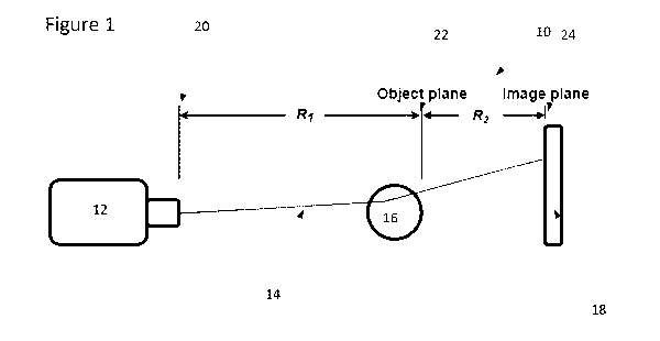
Figure 1 is a schematic diagram of a propagation-based X-ray phase contrast
imaging
system;
Figure 2 is a schematic diagram of a cross-section of the direct-conversion x-
ray detector;
Figure 3 is a photograph of a digital X-ray detector for use in the system of
Figure 1;
Figure 4a is a graph showing DQE vs spatial frequency using the X-ray detector
of Figure
3;
Figure 4b is a graph showing DQE vs spatial frequency using known X-ray
detectors;
Figure 5a is an X-ray image of a bell-pepper seed absorption image with phase
contrast
reduced;
Figure 5b is an X-ray image of a bell-pepper seed absorption image with phase
contrast;
Figure 6 is a schematic diagram of a multilayer detector having layers 1 to N;
Figure 7 is a schematic diagram of a first embodiment of a system
configuration to obtain
multi-energy X-ray images and phase contrast images simultaneously;
Figure 8 is a graph showing penetration depth of x-ray photons in amorphous
selenium
photoconductor material; and
Figure 9 is a flowchart outlining a method of phase contrast X-ray imaging.
Detailed Description of the Disclosure
The disclosure is directed at a method and system for a high-resolution X-ray
detection
for phase contrast imaging. In one embodiment, the system includes an X-ray
source and an X-
3
CA 03079468 2020-04-17
WO 2019/075553 PCT/CA2018/050931
ray detector with a pixel pitch of less than or equal to 25 microns. The X-ray
source is preferably
located a distance R1 from an object plane while the X-ray detector is
preferably located a distance
R2 from the object plane.
Turning to Figure 1, a schematic diagram of a system for high-resolution X-ray
detection
for phase contrast imaging is shown. The system may be seen as a propagation-
based X-ray
phase contract imaging system. In one embodiment, the system enables
propagation-based X-
ray phase contrast imaging (PB-XPC) in a compact, fast manner by approaching
PB-XPC from a
source and detector perspective. The system 10 includes an X-ray source 12
that directs X-rays
(such as in the form of a polychromatic beam 14) towards an object 16 that is
being imaged. The
system further includes a detector 18, located on a side opposite the X-ray
source with respect to
the object 16) to receive, or detect, the X-rays that pass through the object
16 through free-space
propagation. In a preferred embodiment, the X-ray source 12 is a standard
laboratory micro-
focus source and the X-ray detector 18 is a very high resolution and dose
efficient X-ray detector
having a pixel pitch of less than or equal to 25 microns.
As shown in Figure 1, an output plane 20 of the focal spot of the X-ray source
12 is located
a distance R1 from the object plane 22 while an image plane 24 of the X-ray
detector 18 is a
distance R2 from the object plane 22. By selecting a corresponding pixel pitch
(preferably less
than or equal to 25 microns), an optimal (or preferred) R1 (which can be seen
as an X-ray source
focal spot to object plane/source to object distance) and an optimal (or
preferred) R2 (which may
be seen as an object plane to detector image plane/object to detector
distance) may be selected
to achieve, fast, dose efficient PB-XPC using a benchtop device. In one
embodiment, the
selection of the pixel pitch may be based on the X-ray refraction angle of the
X-ray leaving the
object (calculated from the complex refractive index) and the propagation
distance R2. In a
preferred embodiment, a small R2 is more desirable, leading to a deviation of
the X-ray on the
that is detectable by a detector having pixels with a small pixel pitch (such
as less than or equal
to 25 microns).
As was experienced during experiments, the system may detect the minute (in
the range
of 10-5-104 rad) X-ray refraction associated with phase changes encoded by the
object 16.
In one preferred embodiment, the X-ray source 12 may be a standard low-power
(8 VV)
laboratory micro-focus source with a focal spot size of 5 to 9 pm. The focal
spot size is the size
of the X-ray source electron beam that contacts the anode target materials
e.g. tungsten or
molybdenum, which then produces X-rays that propagate to the object 16 and
subsequently to
the detector 18). In current medical imaging solutions, the focal spot size is
0.3 to 1 mm. When
the focal spot is small (such as between 5 to 9 pm), the penumbral blur from
the extent of the
4
CA 03079468 2020-04-17
WO 2019/075553 PCT/CA2018/050931
focal spot is minimized or reduced such that that the X-ray source 12 does not
limit spatial
resolution within the system 10. Given the aim to detect phase changes due to
the object 16, a
coherent or partially coherent incident beam is necessary or preferred. The
lateral coherence
length is proportional to the source-to-object distance, R1, and inversely
proportional to the focal
spot size. That is, a smaller focal spot results in a partially coherent beam
with a smaller R1
distance, or in other words, a more compact system.
One challenge is that a small focal spot in a traditional fixed anode (i.e.
not a costly liquid-
metal jet source), the micro-focus source results in low power output due to
the heat load on the
object. This limitation is a key challenge in obtaining a phase contrast image
in both a short time
and at low x-ray exposures (e.g. to minimize or reduce radiation damage to
objects such as, but
not limited to, biological samples).
Turning to Figure 2, a schematic cross-section of an X-ray detector is shown.
In the
current disclosure, the detector is preferably a high-resolution x-ray
detector based using a direct
conversion photoconductor and complementary metal-oxide semiconductor (CMOS)
pixel
electronics having a pixel pitch of less than or equal to 25 microns.
As shown in Figure 2, the X-ray detector 18 includes a bottom CMOS layer 30
with a
plurality of small sized pixels 32. In the current disclosure, the pixel pitch
of each of the pixels 32
is less than or equal to twenty-five (25) microns. The detector 18 further
includes a
stability/blocking layer 34, a photoconductor layer 36, a blocking layer 38
and an electrode layer
40. The detector 18 may further include a set of bond pads 42 that are used to
enable an electrical
connection for control/data signals.
In one embodiment, the photoconductor layer 36 is an amorphous selenium (a-Se)
photoconductor layer 36. In this embodiment, the blocking layers 34 and 38 on
either side of the
a-Se photoconductor layer 36 may be used to improve mechanical stability of
the detector 18
and/or to reduce the dark current during operation of the detector 18 at high
electric fields. In
another embodiment, the detector 18 may include only one or none of the
blocking layers 34 or
38.
In another embodiment, the stability/blocking layer 34 may be a polyimide
layer that may
function as both, an anticrystallization layer and as a blocking contact on
the bottom of the
photoconductor layer 36. In another embodiment, the blocking layer 38 may be a
parylene layer
that functions as a blocking contact for the photoconductor layer 36. A
contact layer between the
photoconductor layer 36 and the stability/blocking layer may also be, but is
not limited to, a p-type
layer (such as As-doped selenium) or other soft polymer materials. A contact
layer between the
photoconductor layer 36 and the blocking layer 38 may also be, but is not
limited to, a n-type layer
CA 03079468 2020-04-17
WO 2019/075553 PCT/CA2018/050931
such as alkali-metal-doped selenium or cold deposited selenium, or other known
organic and
inorganic hole blocking layers. Although the previous discussion relates to a
direct conversion X-
ray detector, other high-resolution detector technologies, such as indirect
conversion detectors,
or a combination of direct conversion and indirect conversion X-ray detectors
are contemplated.
In direct conversion X-ray detectors, amorphous selenium, silicon, CdZnTe,
CdTe, HgI2,
Pb0, and scintillator infused organic photoconductors such as perovskite
integrated with CMOS
or thin-film-transistor (TFT) pixel arrays may be used for the photoconductor
layer 36. With
indirect conversion X-ray detectors, Csl, LaBr3, and pixelated GOS or Csl
scintillators integrated
CMOS or TFT pixel arrays are may be used.
Excluding x-ray obliquity, which affects both indirect and direct conversion
detectors, the
thickness of the direct conversion photoconductor within the X-ray detector
does not have the
same trade-off with spatial resolution as an indirect conversion
photoconductor because a large
applied electric field transports the X-ray generated charge carriers with
negligible lateral
diffusion.
One advantage of the disclosure is the use of a very fine, or small, pixel
pitch, high dose
efficiency direct conversion X-ray detector to work in conjunction with the
micro-focus source 12
for the PB-XPC approach.
Current X-ray indirect-detection technology exhibits a tradeoff between
spatial resolution
and dose efficiency. The scintillator material used to convert x-rays to
optical photons for detection
by a pixelated matrix of photodiodes results in increased optical scatter with
thickness. Thicker
scintillators absorb more photons but also lead to increased light scattering
while thin scintillators
preserve resolution by limiting scatter but absorb fewer photons and are dose
inefficient reducing
the detective quantum efficiency (DQE). Moreover, trying to visualize very
fine features with lower
spatial resolution detectors requires a large magnification factor which, when
coupled with micro
focal spot (and thus, lower power) X-ray sources additionally leads to longer
scan times and dose.
Turning to Figure 3, a photograph of one embodiment of a pixel pitch imager is
shown.
The pixel pitch imager of Figure 3 is a 5.5um x 6.25 um pixel pitch imager.
Through
experimentation, the dose efficiency measurements were around 10x better than
current systems
and projected results that may be up to 100x better than current detectors by
using pixels having
a size less than or equal to 25 microns. Imaging time can be further reduced
by using high output
micro-focus X-ray tubes (e.g. metal jet X-ray) as the X-ray source, however,
use of a high dose
efficiency detector helps further reduce imaging time (e.g. for high
throughput industrial
applications) and more importantly, to minimize or reduce further radiation
damage to sensitive
biological tissue, especially in life sciences and medical applications.
6
CA 03079468 2020-04-17
WO 2019/075553 PCT/CA2018/050931
Furthermore, in the micrograph of Figure 3, the pixel imager, or hybrid a-
Se/CMOS digital
X-ray detector, the overall chip dimensions are 1.8x3.0 mm2. The a-Se/CMOS
hybrid structure is
visible with a biasing probe for application of positive high voltage to the
gold electrode.
In Figure 4a, which reflect results/measurements using the X-ray detector of
the
disclosure, the DQE calculated for the 70 kVp spectrum using the measured
modulation transfer
function (MTF) and measured noise power spectrum (N PS) are shown. The results
in the 20-60
cycles/mm range exceed all other previously reported X-ray detector DQE
results. Figure 4b
shows a modeled DQE at 70 kVp for an absorption-optimized a-Se photoconductor
layer with a
thickness of 1000-pm assuming no focal spot blur and 100 e- RMS read-out
noise. With optimized
X-ray absorption, the DQE is very high (above 0.5 or 50%) in the 20-60
cycles/mm range. For
the graph of Figure 4b, the photoconductor thickness for the modelled detector
is 1000 microns
while the photoconductor thickness for the detector of Figure 4a was 56
microns.
Using the phase contrast X-ray system of the disclosure, the added detail due
to phase
contrast is demonstrated in Figures 5a and 5b. The hook was used to suspend
the bell pepper
seed which served as the object being imaged. In the case of this phase
contrast image, the
source-to-detector distance was 26 cm (sum of R1 + R2), allowing the images to
be taken in a few
seconds compared to the minutes and hours commonly reported for current phase
contrast
systems. As such, the system of the disclosure may be seen as a highly
compact, fast, low dose
PB-XPC systems. In this experiment, R1 was less than 10 cm for the images
captured (with R2
greater than 0 cm). The R1 values used in the system of the disclosure are in
direct contrast to
current PB-XPC systems which teach away from using R1 values of < 10 cm.
Using the system of the disclosure, phase contrast images were achieved with
R1 values
of <10 cm for a range of R2 values (e.g. between 0 and 200 cm) and pixel sizes
of less than or
equal to 25 microns. In one embodiment, pixels sizes less than 10 microns are
contemplated.
In simulations, a source focal spot of <30 pm was shown to be suitable for
phase contrast
imaging although a focal spot of <10 pm is preferable for sharper images and a
more compact
system.
Turning to Figure 6, a diagram of another embodiment of an X-ray detector for
use with
the system of the disclosure is shown. The X-ray detector 18 of Figure 6 may
be seen as a multi-
layer detector and may enable a compact X-ray imaging system that acquires
both: multi-spectral
(e.g. dual energy spectral X-ray data) as well as a phase contrast image
(including phase retrieval)
simultaneously.
In the current embodiment, the X-ray detector 18 includes a set of conversion
layers 100
(seen as Conversion layer 1, Conversion layer 2, ...Conversion layer N (where
N is any number))
7
CA 03079468 2020-04-17
WO 2019/075553 PCT/CA2018/050931
a set of substrate layers 102 and a set of X-ray filters 104. Different
design/structure of the
conversion layers 100, substrate layers 102 and X-ray filters 104 are
contemplated and Figure
6 provides one such example structure. As will be appreciated, the simplest
implementation of
such a multi-layer detector would include two stacked conversion layers 100
with an intermediate
mid-filter 104. An improved approach could use three stacked conversion layers
with the middle
conversion layer acting as a mid-filter. As will be understood, each of the
conversion layers is
associated with a set of pixels having a size of less than or equal to 25
microns. With N conversion
layers and N set of pixels, N unique data sets may be simultaneously obtained
or generated at a
low object dose i.e. multi-spectral, phase contrast, along with an original
attenuation image.
In the Fresnel region, the "transport of intensity equation" (TIE) implies
that contrast from
intensity variations at the image plane is proportional to the propagation
distance from the object
plane and the spatial gradient of the phase distribution in the object plane.
This differential phase
contrast results in an "edge-enhancement" effect due to phase changes being
most abrupt at the
edges of the object where there is a rapid change in the refractive index.
Although the use of PB-
XPC X-ray imaging results in increased contrast at object boundaries for
better detectability of
materials with poor x-ray absorption, the relationship between the physical
geometry of the object
and its visualization in the image plane is more complicated.
Specifically, the boundaries in the image may not correspond exactly to
boundaries in the
object. To restore quantitative boundary information in the image, a "phase
retrieval"
reconstruction is typically required to be performed. One method for phase
retrieval is a "direct
approach" by solving the deterministic TIE for x-ray intensity and phase
information in the object
plane. Being non-iterative and numerically efficient this method is viable for
use in projection
imaging and for 3D micro-CT.
The TIE, for a single wavelength, includes one known variable (intensity in
the image
plane) and two unknown variables (intensity and phase in the object plane). In
the case of a pure
phase (i.e. no absorption) or homogenous object and monochromatic radiation,
the solution to
the TIE is relatively straightforward. For this case, in the geometric optics
approximation, the
intensity and phase in the object plane are related and a unique solution to
the TIE can be
obtained from a single measurement in the image plane or alternately, a single
image acquisition.
For general inhomogeneous objects (i.e. the more practical situation) with
uncorrelated
absorption and refraction properties, at least two measurements at different
image planes or
different radiation wavelengths are required to solve the system of equations.
This requirement
poses a challenge for radiation dose sensitive (life sciences or medical) or
even high throughput
(e.g. real-time) applications where the time taken to move the detector to
acquire the two
8
CA 03079468 2020-04-17
WO 2019/075553 PCT/CA2018/050931
measurements (i.e. images) necessary for phase retrieval is prohibitive. As
such, the system of
the disclosure allows for multiple images to be retrieved with a lower dose
exposure for the object.
Moreover, most practical applications (e.g. biomedical clinical imaging or
even in industrial
inspection) require the use of commonly available polychromatic x-ray sources,
which makes
obtaining the conventional TIE solution problematic since it inherently
assumes a monochromatic
source.
To overcome the above challenges of obtaining at least two measurements to
solve the
TIE with monochromatic and/or polychromatic sources, the multilayer (i.e.
stacked) X-ray detector
of Figure 6 may be used to simultaneously capture multiple images at different
image planes with
adaptable X-ray spectra for PB-XPC. A multilayer detector typically includes a
plurality of stacked
x-ray conversion layers on optional substrates with optional intermediate x-
ray filter materials
(such as schematically shown in Figure 6), where critically, each conversion
layer captures
information in a different image plane.
Each conversion layer can be a direct conversion layer (such as the proposed
fine pitch
a-Se direct conversion X-ray detector) or an indirect conversion layer. In a
direct conversion layer,
an X-ray semiconductor (e.g. amorphous selenium, silicon, Pb0, HgI2, CdZnTe,
CdTe, organic
semiconductor with nanoparticles, etc.) converts incident X-ray photons
directly into electronic
charge. The X-ray semiconductor can be optionally paired with a readout
electronics plane (e.g.
thin film transistor array, CMOS pixel array) that contains an active matrix
array of readout pixels
(transistors and/or storage capacitor). In certain cases, the X-ray
semiconductor and readout
electronics plane are both part of the X-ray conversion layer.
In an indirect X-ray conversion layer, the scintillator material (e.g. GOS,
Csl, Nal, CaW04,
LYSO, etc.) is used to convert incident X-ray photons into optical photons,
which are then detected
by an underlying pixelated photosensitive readout electronics plane. The
photosensitive readout
electronics plane could be a large area active matrix array of pixels (e.g.
containing a photodiode
with thin film transistors or a photodiode with an active pixel sensor) made
of a variety of materials
including large area thin film inorganic (e.g. amorphous silicon, metal oxide,
LTPS, continuous
grain silicon, crystalline silicon) or even organic semiconductors. In this
embodiment, the
scintillator and photosensitive readout electronics can both be part of the X-
ray conversion layer.
Due to the greater penetration depth of higher energy photons relative to
lower energy
photons (e.g. see Figure 8 for penetration depth in amorphous selenium
semiconductor), a single
x-ray exposure results in each X-ray conversion layer acquiring an image with
a different x-ray
spectrum. The X-ray spectra can be controlled using the thickness of each
conversion layer (i.e.
the semiconductor layer in direct conversion or the scintillator layer in
indirect conversion) and/or
9
CA 03079468 2020-04-17
WO 2019/075553 PCT/CA2018/050931
the filter layer. Characterization of the spectra (without an object) may be
necessary for phase
retrieval.
In one embodiment, the penetration depth is equal to the reciprocal of the X-
ray
attenuation coefficient and corresponds to the depth within a material that
the x-ray intensity
reduces to -37% of its initial value. The discontinuity at -12.7 keV is due to
photoelectric
absorption.
Filter materials can range from common metal mid-filters, such as aluminum and
copper.
If an additional X-ray conversion layer is used as the filter, then, in this
case, there would be three
X-ray conversion layers stacked on top of each other. In principle, at least
two X-ray conversion
layers are necessary but additional layers can be stacked as necessary to
obtain additional
spectral separation, which could improve phase retrieval by allowing the use
of more accurate
reconstruction formulae.
Even further spectral separation could be obtained by modulating the X-ray
semiconductor
thickness in any given direct X-ray conversion layer on a pixel by pixel basis
or alternately,
modulating the scintillator thickness in any given indirect X-ray conversion
layer on a pixel by pixel
basis. By modulating the thickness of the X-ray conversion layer at the pixel
level, spatial
resolution can be a trade-off to obtain extra spectral separation even in a
single layer.
Using very small pixel pitch dimensions (as with our fine pixel pitch detector
having pixel
sizes less than or equal to 25 microns) in each conversion layer can further
improve performance
by detecting the small refraction angle of x-rays (which is necessary for
phase contrast) at shorter
propagation distances from object plane to image plane. X-ray intensity (and
therefore signal-to-
noise ratio) decreases with the inverse square of propagation distance, so
reducing propagation
distance can lower dose as well as potentially speed up phase retrieval
compared to other
propagation-based methods or other phase contrast imaging modalities (e.g.
grating based.)
In another embodiment, to obtain both multi-spectral and phase retrieval data
for PB-XPC,
the system may include two different X-ray sources in conjunction with two
fine-pitch single layer
X-ray detectors that are operating in different planes as schematically shown
in Figure 7. As will
be understood, a fine-pitch single layer X-ray detector is one with pixels
having a size less than
or equal to 25 microns.
As shown in Figure 7, the system includes a first X-ray source 150 that
directs a
polychromatic beam towards an object 152 that is then detected by a first X-
ray detector 154.
The system further includes a second X-ray source 156 that directs a
polychromatic beam
towards the object 152 that is then detected by a second X-ray detector 158.
In one embodiment,
the distance between the first X-ray source 150 and the object plane (Rim or
CA 03079468 2020-04-17
WO 2019/075553 PCT/CA2018/050931
R1_1) and the distance between the second X-ray source 156 and the object
plane (R1 D2 or R1_2)
may be set to the same value while the distance between the object plane and
the image plane
of the first X-ray detector 154 (R2D1 or R1_2) and the distance between the
image plane of the
second X-ray detector 158 and the object plane (R1 D2 or R2_2) may be set to
different values.
The two set of X-ray source and X-ray detector pairs allow the system to
obtain multiple two-
dimensional (2D) images from the first and second X-ray detectors. In an
alternate
embodiment, the beams of the first X-ray source and the second X-ray source
shine X-ray are
directed towards the object in non-parallel directions. In another embodiment,
the beams of the
first X-ray source and the second X-ray source are directed towards the object
in perpendicular
directions.
In both embodiments where multiple images are generated or detected, they may
then be
combined in any known methodologies to obtain a single overall image (if
required) using
reconstruction algorithms.
One advantage of the system of Figure 7 is that the X-ray spectrum from the
first X-ray
source 150 and the X-ray spectrum from the second X-ray source 156 may be
defined
independently of the first X-ray detector 154 and the second X-ray detector
158 leading to
additional simplicity in the reconstruction algorithms. As before, the system
configuration of
Figure 7 may enable acquisition of phase contrast images, phase retrieval,
multi-spectral images
and conventional attenuation images in a single scan. To obtain a three-
dimensional (3D) image,
either the object or the source/detector pairs can be rotated to obtain
multiple projections for
reconstruction or further X-ray source/X-ray detector pairs may be used.
Turning to Figure 9, a flowchart outlining a method of phase contrast imaging
is shown.
Initially, an X-ray source is placed a distance R1 away from the object being
imaged (900). This
distance is preferably less than 10cm and, in one embodiment, is measured from
the focal spot
of the X-ray source to the object plane of the object. An X-ray detector is
then placed a distance
R2 from the object (902) on a side of the object opposite the location of the
X-ray source. This
distance is preferably between Ocm and 200cm and, in one embodiment, is
measured from the
object plane to a detector plane.
The X-ray source then directs a polychromatic beam towards the object (904).
The
resulting photons are then detected by the X-ray detector via its set of
pixels that are sized to be
less than or equal to 25 microns (906). If necessary, further X-ray source and
X-ray detector pairs
may be placed (908) around the object to obtain multiple images with a lower
radiation dose.
While the current disclosure has been directed at a compact phase contrast X-
ray detector
with direct conversion selenium-CMOS detectors, other direct conversion
materials such as HgI2,
11
CA 03079468 2020-04-17
WO 2019/075553 PCT/CA2018/050931
CZT, TIBr, and silicon can be employed in place of selenium and the CMOS
pixels could be
replaced by poly-Si, metal-oxide, or common II-VI or III-V semiconductors.
Moreover, high-
resolution indirect-conversion X-ray detectors (e.g. with thin scintillators,
or pixelated scintillators)
can also be employed albeit likely with lower dose efficiency than direct
conversion detectors.
Micro-computed-tomography (microCT) is also possible with this system by
adding a rotational
stage (or creating a rotating gantry) for generating multiple x-ray projection
images of the object
from different perspectives, and CT reconstruction software.
In addition to providing fast imaging in a compact system, the system of the
disclosure
also has a significant benefit for micro-anatomical imaging to visualize
greater level of detail and
avoid damaging DNA by using less X-ray radiation to acquire an image. As an
example, since
detailed knowledge of genes and the ability to control gene expression is
available in mice and
rats, the ability to quantitate the impact of highly targeted genetic
manipulations on organ structure
and function using phase contrast micro-CT could help answer how genes link to
whole body
pathophysiology. The combination of better visualization of soft tissue using
phase contrast X-ray
and high detector dose efficiency can fundamentally advance genomics by
allowing high
resolution, non-invasive and non-destructive imaging in live, intact animals
and plants, tissues,
and even single cells - tasks that are not possible using other techniques.
Similar advantages
exist for other scientific and non-destructive imaging applications for
example, imaging agricultural
products, plastics, polymers and various nano-composite materials and glasses.
In the preceding description, for purposes of explanation, numerous details
are set forth
in order to provide a thorough understanding of the embodiments. However, it
will be apparent to
one skilled in the art that these specific details may not be required. In
other instances, well-known
structures may be shown in block diagram form in order not to obscure the
understanding. For
example, specific details are not provided as to whether elements of the
embodiments described
herein are implemented as a software routine, hardware circuit, firmware, or a
combination thereof.
Embodiments of the disclosure or components thereof can be provided as or
represented
as a computer program product stored in a machine-readable medium (also
referred to as a
computer-readable medium, a processor-readable medium, or a computer usable
medium having
a computer-readable program code embodied therein). The machine-readable
medium can be
any suitable tangible, non-transitory medium, including magnetic, optical, or
electrical storage
medium including a diskette, compact disk read only memory (CD-ROM), memory
device (volatile
or non-volatile), or similar storage mechanism. The machine-readable medium
can contain
various sets of instructions, code sequences, configuration information, or
other data, which,
when executed, cause a processor or controller to perform steps in a method
according to an
12
CA 03079468 2020-04-17
WO 2019/075553 PCT/CA2018/050931
embodiment of the disclosure. Those of ordinary skill in the art will
appreciate that other
instructions and operations necessary to implement the described
implementations can also be
stored on the machine-readable medium. The instructions stored on the machine-
readable
medium can be executed by a processor, controller, or other suitable
processing device, and can
interface with circuitry to perform the described tasks.
The above-described embodiments are intended to be examples only. Alterations,
modifications and variations can be effected to the particular embodiments by
those of skill in the
art without departing from the scope, which is defined solely by the claims
appended hereto.
13