Note: Descriptions are shown in the official language in which they were submitted.
SYSTEM AND METHOD FOR MITIGATING BROADBAND INTERFERENCE
BACKGROUND
Statement of the Technical Field
[0001] The present document concerns communication systems. More
particularly, the
present document concerns systems and methods for mitigating interference
(e.g., broadband
and/or narrowband) in receivers.
Description of the Related Art
[0002] Conventional radios include Land Mobile Radios ("LMRs"). When LMRs
get
close to broadband sites operating in neighboring frequency allocations, they
experience
relatively high levels of the broadband signal as interference. This
interference can produce
significant intermodulation ("TM") products which may degrade radio
performance or
sensitivity by raising the noise floor of the receiver. These effects are
further aggravated by
the high peak to average power ratio characteristics of broadband signals.
SUMMARY
[0003] This document concerns systems and methods for operating a
communication
device so as to mitigate intermodulation interference (e.g., broadband and/or
narrowband) to
a signal. The methods comprise: continuously monitoring several communication
channels
by the communication device; using a noise floor level estimate of the
communication device
to detect when the communication device is under an influence of high
interference;
determining an optimal level of attenuation to be applied by a variable
attenuator of the
communication device's receiver so as to mitigate the influence of
intermodulation
interference due to the interference signal; and selectively adjusting an
amount of attenuation
being applied by the variable attenuator to achieve the optimal level of
attenuation for best
receiver performance.
[0004] In some scenarios, the methods also comprise: estimating the noise
floor level
with an original attenuation level being applied by the variable attenuator of
the
communication device's receiver. The noise floor level is estimated by
acquiring a power
measurement value for an on channel, a power measurement value for at least
one high side
channel, and a power measurement value for at least one low side channel. A
same or
1
Date Recue/Date Received 2020-06-22
different number of high channel power measurements and low channel power
measurements
may be acquired. The noise floor level is set equal to a minimum value of the
power
measurement values acquired for the measured channels over the receiver's
analysis
bandwidth (e.g., in some scenarios the following channels will be measured as
a minimum:
the on channel, at least one high side channel, and at least one low side
channel will be
measured).
[0005] In those or other scenarios, a detection is made as to when the
communication
device is under the influence of a high level of interference based on results
from comparing
the estimated noise floor level to a threshold value. The threshold value is
equal to a known
thermal noise floor level plus a certain amount X. The certain amount X
variable represents
the amount of noise floor increase allowed before a test is performed to
determine if the
interference is due to intermodulation and the receiver sensitivity can be
improved by adding
some attenuation before a low noise amplifier to put the receiver in a more
linear operating
region.
[0006] The optimal level of attenuation is determined by: iteratively
adding an
incremental level of attenuation (A attenuation) and measuring the noise level
difference (A
noise power) from the previous iteration; calculating a slope that is defined
by a change in
noise power over a change in attenuation; comparing the slope to a threshold
value Y; and
considering the optimal level of attenuation to be the previous level of
attenuation applied by
the variable attenuator when the current slope estimate is less than the
threshold value Y.
BRIEF DESCRIPTION OF THE DRAWINGS
[0007] This disclosure is facilitated by reference to the following drawing
figures, in
which like numerals represent like items throughout the figures.
[0008] FIG. 1 is an illustration of an illustrative system implementing the
present
solution.
[0009] FIG. 2 is an illustration of an illustrative communication device
architecture.
[0010] FIG. 3 is an illustration of an illustrative receiver architecture.
[0011] FIG. 4 is a graph that is useful for understanding LTE interference
in an LMR
band.
2
Date Recue/Date Received 2020-06-22
[0012] FIG. 5 is a graph that is useful for understanding the present
solution.
[0013] FIG. 6 is a flow diagram of a method for mitigating LTE
interference.
[0014] FIG. 7 is a flow diagram of a method for mitigating LTE
interference.
[0015] FIG. 8 an illustration that is useful for determining whether an
estimate noise floor
exceeds a threshold value.
[0016] FIGS. 9-10 each provide a graph that is useful for understanding the
present
solution.
DETAILED DESCRIPTION
[0017] It will be readily understood that the solution described herein and
illustrated in
the appended figures could involve a wide variety of different configurations.
Thus, the
following more detailed description, as represented in the figures, is not
intended to limit the
scope of the present disclosure, but is merely representative of certain
implementations in
various different scenarios. While the various aspects are presented in the
drawings, the
drawings are not necessarily drawn to scale unless specifically indicated.
[0018] Reference throughout this specification to features, advantages, or
similar
language does not imply that all of the features and advantages that may be
realized should be
or are in any single embodiment of the invention. Rather, language referring
to the features
and advantages is understood to mean that a specific feature, advantage, or
characteristic
described in connection with an embodiment is included in at least one
embodiment of the
present invention. Thus, discussions of the features and advantages, and
similar language,
throughout the specification may, but do not necessarily, refer to the same
embodiment.
[0019] This document generally concerns systems and methods for operating a
communication device so as to mitigate intermodulation interference (e.g.,
broadband and/or
narrowband) to a receiver. The methods comprise: continuously monitoring a
plurality of
communication channels by the communication device; using a noise floor level
estimate of
the communication device to detect when the communication device is under an
influence of
high interference; determining an optimal level of attenuation to be applied
by a variable
attenuator of the communication device's receiver so as to mitigate the
influence of
intermodulation interference due to the interference signal; and selectively
adjusting an
3
Date Recue/Date Received 2020-06-22
amount of attenuation being applied by the variable attenuator to achieve the
optimal level of
attenuation for best receiver performance in the presence of the interfering
signal.
[0020] In some scenarios, the methods also comprise: estimating the noise
floor level
with an original attenuation level being applied by the variable attenuator of
the
communication device's receiver. The noise floor level is estimated by
acquiring a power
measurement value for an on channel, a power measurement value for at least
one high side
channel, and a power measurement value for at least one low side channel. A
same or
different number of high channel power measurements and low channel power
measurements
may be acquired. The noise floor level is set equal to a minimum value of the
power
measurement values acquired for the measured channels (e.g., an on channel, at
least one
high side channel, and at least one low side channel) over the receiver's
analysis bandwidth.
[0021] In those or other scenarios, a detection is made as to when the
communication
device is under the influence of a high level of interference based on results
from comparing
the noise floor level estimate to a threshold value. The threshold value is
equal to a known
thermal noise floor level plus a certain amount X. The certain amount X
variable represents
the amount of noise floor increase that is allowed before an attenuation test
is performed to
determine if the interference is due to intermodulation and the receiver
sensitivity can be
improved by adding some attenuation before a low noise amplifier to put the
receiver in a
more linear operating region.
[0022] The optimal level of attenuation is determined by: iteratively
adding an
incremental level of attenuation (A attenuation) and measuring the noise level
difference (A
noise power) from a previous iteration; calculating a slope that is defined by
a change in
noise power over a change in attenuation; comparing the slope to a threshold
value Y; and
considering the optimal level of attenuation to be the previous level of
attenuation (e.g., a(n-
1)) applied by the variable attenuator when the current slope estimate is less
than the
threshold value Y
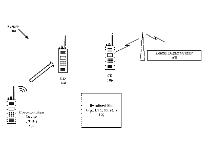
[0023] Referring now to FIG. 1, there is provided an illustration of an
illustrative system
100. System 100 comprises a plurality of communication devices 102, 104, 106,
a Central
Dispatch Center ("CDC") 108, and a broadband site 110. The communication
devices 102-
106 include, but are not limited to, a portable radio (e.g., an LMR), a fixed
radio with a static
location, a smart phone, and/or a base station. The broadband site 110
includes, but is not
limited to, an LMR site, a 2G cellular site, a 3G cellular site, a 4G cellular
site, and/or a 5G
4
Date Recue/Date Received 2020-06-22
cellular site. CDC 108 and broadband site 110 are well known in the art, and
therefore will
not be described herein.
[0024] During operation of system 100, signals are communicated between the
communication devices 102-106 and/or between one or more communication devices
and the
CDC 108. For example, communication device 102 communicates a signal to
communication device 104, and CDC 108 communicates a signal to communication
device
106. Communication devices 104 and 106 perform operations to mitigate
interference caused
by the broadband site 110. The interference results because the raised noise
floor of received
broadband signals (e.g., broadband signal 400 of FIG. 4) causes the noise
floor of the
communication device to be increased when the signal power is above a certain
level. The
manner in which communication devices 104 and 106 mitigate the broadband
interference to
signals will become evident as the discussion progresses.
[0025] Referring now to FIG. 2, there is provided an illustration of an
illustrative
architecture for a communication device 200 which is configured for carrying
out the various
methods described herein for mitigating the broadband interference.
Communication devices
102-106 are the same as or similar to communication device 200. As such, the
discussion
provided below in relation to communication device 200 is sufficient for
understanding
communication devices 102-106. Communication device 200 can include more or
less
components than that shown in FIG. 2 in accordance with a given application.
For example,
communication device 200 can include one or both components 208 and 210. The
present
solution is not limited in this regard.
[0026] As shown in FIG. 2, the communication device 200 comprises an LMR
communication transceiver 202 coupled to an antenna 216. The LMR communication
transceiver can comprise one or more components such as a processor, an
application specific
circuit, a programmable logic device, a digital signal processor, or other
circuit programmed
to perform the functions described herein. The communication transceiver 202
can enable
end-to-end LMR communication services in a manner known in the art. In this
regard, the
communication transceiver can facilitate communication of voice data from the
communication device 200 over an LMR network.
[0027] Although the communication device 200 has been described herein as
comprising
an LMR communication transceiver, it should be understood that the solution is
not limited in
this regard. In some scenarios, the communication network can comprise a
cellular
Date Recue/Date Received 2020-06-22
communication network instead of an LMR type network. In that case, the
communication
device 200 could include a cellular network communication transceiver in place
of an LMR
communication transceiver. In another scenario, the communication device 200
could
include both an LMR communication transceiver and a cellular network
communication
transceiver. In this regard, it should be understood that the solutions
described herein can be
implemented in an LMR communication network, a cellular communication network,
and/or
any other communication network where broadband interference by another
communication
system exists that generates interference energy that may be detected in
neighboring
channels.
[0028] The LMR communication transceiver 202 is connected to a processor
204
comprising an electronic circuit. During operation, the processor 204 is
configured to control
the LMR communication transceiver 202 for providing LMR services. The
processor 204
also facilitates mitigation of interference to signals. The manner in which
the processor
facilitates interference mitigation will become evident as the discussion
progresses.
[0029] A memory 206, display 208, user interface 212 and Input/Output
("I/O") device(s)
210 are also connected to the processor 204. The processor 204 may be
configured to collect
and store data generated by the I/O device(s) 210 and/or external devices (not
shown). Data
stored in memory 206 can include, but is not limited to, one or more look-up
tables or
databases which facilitate selection of communication groups or specific
communication
device. The user interface 212 includes, but is not limited to, a plurality of
user depressible
buttons that may be used, for example, for entering numerical inputs and
selecting various
functions of the communication device 200. This portion of the user interface
may be
configured as a keypad. Additional control buttons and/or rotatable knobs may
also be
provided with the user interface 212. A battery 214 or other power source may
be provided
for powering the components of the communication device 200. The battery 200
may
comprise a rechargeable and/or replaceable battery. Batteries are well known
in the art, and
therefore will not be discussed here.
[0030] The communication device architecture show in FIG. 2 should be
understood to
be one possible example of a communication device system which can be used in
connection
with the various implementations disclosed herein. However, the systems and
methods
disclosed herein are not limited in this regard and any other suitable
communication device
system architecture can also be used without limitation. Applications that can
include the
6
Date Recue/Date Received 2020-06-22
apparatus and systems broadly include a variety of electronic and computer
systems. In some
scenarios, certain functions can be implemented in two or more specific
interconnected
hardware modules or devices with related control and data signals communicated
between
and through the modules, or as portions of an application-specific integrated
circuit. Thus,
the illustrative system is applicable to software, firmware, and hardware
implementations.
[0031] Referring now to FIG. 3, there is provided a more detailed
illustration of an
illustrative receiver portion 300 of the LMR communication transceiver 202.
Receiver 300
comprises a variable attenuator 302, a band selection filter 303, a Low-Noise
Amplifier
("LNA") 304, front end hardware 306, and back end hardware 308. Each of the
listed
devices is known in the art, and therefore will not be described herein.
Still, it should be
noted that the variable attenuator receives signals from the antenna 216 and
applies
attenuation to the place the receiver 300 in a more linear operating region.
The amount of
attenuation is controlled by the processor 204 of FIG. 2. The manner in which
the attenuation
by the variable attenuator 302 is controlled will become evident as the
discussion progresses.
[0032] Referring now to FIG. 4, there is provided a graph that is useful
for understanding
how the noise interference is caused by an LTE signal 400 in the LMR band 402.
Spectrum
404 represents the relative power of the noise interference that is caused by
a spreading of the
LTE signal 400 into the LMR band 402. This additional noise that shows up at
the receiver's
front end degrades the performance of the receiver. Spectrum 406 represents
the noise
interference when both LMR carriers and the LTE signal 400 are present in the
LMR band
402. In this case, there is an even higher interference to signals in the
receiver band. This
apparent noise exists because of a limitation in a performance of the
receiver. If a signal
which is higher than the linear operating region of the receiver and causing
intermodulation
interference is attenuated prior to the receiver's front end, the noise floor
drops rapidly. For
example, if 1 dB of attenuation is added in the receiver, then the noise floor
decreases by 3
dB if the interference is domination by 3rd order intermodulation products.
Thus, an
advantage is obtained by attenuating the signal because the interference
generated by
intermodulation is more attenuated.
[0033] Referring now to FIG. 5, there is provided a graph showing a current
performance
of an LMR receiver when no attenuation is applied prior to its front end
hardware. The
current performance is represented by line 500. Line 500 has a slope of 3:1.
The slope is
defined as the change in noise power over the change in attenuation (i.e., A
noise power/A
7
Date Recue/Date Received 2020-06-22
attenuation). The 3:1 slope is due to the 3rd order IM products caused by an
LTE site's signal
level placing the communication device receiver in a non-linear operating
region. Line 502
represents the desired performance of the LMR receiver with an optimal amount
of
attenuation added to its front end. Line 502 has a slope of 1:1, which
indicates that the LMR
receiver is operating in a more linear operating region. Line 504 represents
the LMR receiver
performance when a 6 dB attenuation is applied to its front end. As can be
seen, there is a 12
dB improvement in LMR receiver performance when the 6 dB attenuation is
applied to its
front end. Line 506 represent the LMR receiver performance when a 12 dB
attenuation is
applied. As can be seen, there is an 18 dB improvement in LMR receiver
performance when
the 12 dB attenuation is applied to its front end.
[0034] Notably, the attenuation should not be continuously applied at the
receiver front
end to mitigate the LTE interference because some sensitivity of the receiver
would be lost
during times when the IM condition does not exit. So, the present solution
waits until the
measured slope p is less than the threshold parameter Y.
[0035] Referring now to FIG. 6, there is provided a method 600 for
mitigating LTE
interference. Method 600 begins with 602 and continues with 604 where a
communication
device (e.g., communication device 104 or 106 of FIG. 1) performs operations
to
continuously monitor a communications channel. Methods for monitoring
communications
channels are well known in the art, and therefore will not be described
herein. The
communication device also receives noise signals and/or communications signals
in 604.
Methods for receiving noise signals and communications signals are well known
in the art,
and therefore will not be described herein.
[0036] In 606, the noise floor level of the communication device is used to
detect when
the communication device is under the influence of IM interference or in an IM
limited
condition. The manner in which the noise floor level is used here will become
more evident
as the discussion progresses. If the communication device is under the
influence of IM
interference, then an optimal level of attenuation that is to be applied by a
variable attenuator
(e.g., variable attenuator 302 of FIG. 3) is determined as shown by 608. In
610, the amount
of attenuation being applied by the variable attenuator is selectively
adjusted based on the
optimal level of attenuation. For example, the level of attenuation being
applied by the
variable attenuator is set equal to the optimal level of attenuation.
Subsequently, 612 is
performed where method 600 ends or other processing is performed (e.g., return
to 602).
8
Date Recue/Date Received 2020-06-22
[0037] Referring now to FIG. 7, there is provided an illustrative method
700 for
mitigating LTE interference. Method 700 includes operations 702-724 to
determine when a
communication device is in an environment where the performance is limited by
IM products
and not thermal noise regardless of what the measured on-channel and adjacent
channel
powers are. This determination is made based on an estimate noise floor of the
communication device's receiver. Notably, operations in box 750 are performed
to detect
when there is a high level of interference. Operations in box 752 are
performed to determine
if the inference is due to IM and to change the attenuation to the optimal
level to mitigate the
IM. All or some of the operations 702-724 can be performed by a communication
transceiver
(e.g., LMR communication transceiver 202 of FIG. 2) and/or a processor (e.g.,
processor 204
of FIG. 2) of a communication device (e.g., communication device 102-106 of
FIG. 1, or
communication device 200 of FIG. 2).
[0038] As shown in FIG. 7, method 700 begins with 702 and continues with
704 where a
communication device (e.g., communication device 104 or 106 of FIG. 1)
performs
operations to continuously monitor a communications channel. Methods for
monitoring
communications channels are well known in the art, and therefore will not be
described
herein. The communication device also receives noise signals and/or
communications signals
in 704. Methods for receiving noise signals and communications signals are
well known in
the art, and therefore will not be described herein.
[0039] Next in 706, the communication device estimates a noise floor k with
an original
attenuation level (e.g., zero) being applied by a variable attenuator (e.g.,
variable attenuator
302 of FIG. 3) of the communication device's receiver (e.g., receiver 300 of
FIG. 3). The
noise floor estimation is achieved in accordance with a process shown in FIG.
8. As shown
in FIG. 8, the process begins by acquiring a measurement of an on channel
power Po in 802,
at least one measurement of a high side channel power P+i, . . ., P+Q as shown
by 804-806,
and at least one measurement of a low side channel power Pi, . . ., P_w as
shown by 808-810.
Q and Ware any integer values. Q and W can have the same or different value.
Techniques
for acquiring channel power measurements are well known in the art, and
therefore will not
be described here. The power measurements are then used in 808 to determine a
noise floor
estimate k. The noise floor estimate k may by example be set equal to the
minimum acquired
power measurement value Prnin. Next, the noise floor estimate k is compared to
a threshold
value thr in 812. The threshold value thr is equal to a thermal noise floor
level (which
depends on the channel bandwidth the noise measurement is performed over) plus
X dB.
9
Date Recue/Date Received 2020-06-22
[0040] X dB is selected based on a given application. The level X is the
amount of
degradation that is allowed before the attenuation test for the existence of
IM is performed
and will vary with specific applications and equipment properties
[0041] Referring now to FIG. 9, a chart is provided that shows that a high
side channel in
box 900 is an interfering adjacent channel, the on channel in box 902 has a
low signal (e.g.,
due to being far away), and the low channel in box 904 has the smallest power
level. In this
scenarios, the noise floor estimate k is set equal to the power level of the
low channel since it
is the minimal power level of the three channels. The present solution is not
limited to the
particulars of this scenario.
[0042] If the noise floor estimate k is greater than the threshold value
thr, then an
assumption is made that the signal is in a non-linear region of the receiver
and is generating
IM (e.g., has at least a 3:1 slope). At this time, a test is performed in
method 700 to
determine if an increased amount of attenuation (e.g., 1 dB) improves the
communication
device's receiver sensitivity, i.e., whether the noise floor level estimate is
decreased more
than Y times the amount of the added attenuation.
[0043] Referring again to FIG. 7, the result R is used in 708 to determine
whether the
estimate noise floor k has increased a certain amount above the threshold thr.
If not
[708:N0], then method 700 returns to 706. If so [708:YES], then method 700
continues with
710.
[0044] In 710, an amount of attenuation applied by the variable attenuator
(e.g., variable
attenuator 302 of FIG. 3) of the communication device's receiver (e.g.,
receiver 300 of FIG.
3) is changed by a given amount (e.g., > 1 dB) to improve the communication
device's
sensitivity. Typical 3rd order IM products have a 3 x increase in the noise
level for a 1 x
increase in the signal level. Typical 5th order IM products have a 5 x
increase in the noise
level for a 1 x increase in the signal level.
[0045] Next in 712, a new noise floor level k' of the communication device
is estimated
with added attenuation. 712 can also involve measuring the difference between
the new
noise floor level k' and the previous noise floor level k. Upon completing
712, method 700
continues with 716. In 716, a slope p of the signal is calculated. Methods for
computing the
slope p of the signal are well known in the art, and therefore will not be
described herein.
Still, it should be understood that the slope p is the change in noise power
over the change in
Date Recue/Date Received 2020-06-22
attenuation. If the slope p is less than Y [718:YES1, then method 700 returns
to 706 as shown
by 720. If the slope p is greater than Y [718:N01, then an assumption is made
that signal
degradation is occurring due to the IM effects. Y is an integer (e.g., 1, 2,
etc.). Accordingly,
722 is performed where the attenuation is set for the signal to the previous
level of
attenuation (e.g., a(k-1), i.e., the original attenuation level plus a total
amount of added
attenuation) to benefit the sensitivity of the receiver. Subsequently, 724 is
performed where
method 700 ends or other processing is performed (e.g., return to 702).
[0046] Referring now to FIG. 10, there is a graph showing results from
operating an
LMR receiver in accordance with the above described method for mitigating LTE
interference. As can be seen in FIG. 10, an 18 dB noise floor reduction is
provided when 6
dB of attenuation to the LMR receiver's front end. This 18 dB noise floor
reduction results in
an improvement in the LMR receiver's sensitivity.
[0047] The described features, advantages and characteristics disclosed
herein may be
combined in any suitable manner. One skilled in the relevant art will
recognize, in light of
the description herein, that the disclosed systems and/or methods can be
practiced without
one or more of the specific features. In other instances, additional features
and advantages
may be recognized in certain scenarios that may not be present in all
instances.
[0048] As used in this document, the singular form "a", "an", and "the"
include plural
references unless the context clearly dictates otherwise. Unless defined
otherwise, all
technical and scientific terms used herein have the same meanings as commonly
understood
by one of ordinary skill in the art. As used in this document, the term
"comprising" means
"including, but not limited to".
[0049] Although the systems and methods have been illustrated and described
with
respect to one or more implementations, equivalent alterations and
modifications will occur
to others skilled in the art upon the reading and understanding of this
specification and the
annexed drawings. In addition, while a particular feature may have been
disclosed with
respect to only one of several implementations, such feature may be combined
with one or
more other features of the other implementations as may be desired and
advantageous for any
given or particular application. Thus, the breadth and scope of the disclosure
herein should
not be limited by any of the above descriptions. Rather, the scope of the
invention should be
defined in accordance with the following claims and their equivalents.
11
Date Recue/Date Received 2020-06-22