Note: Descriptions are shown in the official language in which they were submitted.
1
CA 03085830 2020-06-15
WO 2019/176360 PCT/JP2019/003638
Description
Title of Invention: OPTICAL DEVICE RANGE SENSOR USING
OPTICAL DEVICE, AND MOBILE OBJECT
Technical Field
[0001] Embodiments of the present disclosure relate to an optical device
that scans a laser
beam, a range sensor provided with the optical device, and a mobile object.
Background Art
[0002] In the operations of a mobile object such as a vehicle, a ship, and
an aircraft, tech-
nologies to detect the position of an object in a wide range of angle arc
used. As one
example of such sensing technologies, light detection and ranging (LiDAR) is
known
in the art. The LiDAR is remote sensing based on light, and uses time-of-
flight (TOF)
method in which the distance to the object is measured based on the length of
time it
takes while the laser beams that are emitted from the laser beam source are
reflected by
an object and then return to the sensor. The laser beams are scanned in a wide
angle by
a scanner such as a micro-electromechanical systems (MEMS) mirror and a
polygon
mirror. As known in the art, edge-emitting semiconductor laser that emits
laser beams
parallel to the substrate is used as a LiDAR laser beam source. As it is
difficult to
integrate such edge-emitting semiconductor laser, the use of a vertical-cavity
surface-
emitting laser (VCSEL) device as a light source is under study as the multiple
light
emitting elements of the VCSEL device can easily be integrated into the same
substrate. The VCSEL device performs lasing in a direction perpendicular to
the
substrate. A configuration in which the laser beams that are emitted from a
plurality of
light-emitting points are focused on the surface of a movable mirror using a
VCSEL
array and are optically scanned by the movable mirror is known in the art
(see, for
example, PTL 1).
Citation List
Patent Literature
[0003] PTL 1: Japanese Patent Application Publication No. 2010-151958
Summary of Invention
Technical Problem
[0004] In the known optical scanners, laser beams are scanned as the light
emitted from the
VCSEL device is directly focused on a movable mirror by an optical element
such as a
focus lens. Since the output power of each light emitting element is small,
the output
power of the VCSEL device is increased by two-dimensional integration of the
light
emitting elements.
2
CA 03085830 2020-06-15
WO 2019/176360 PCT/JP2019/003638
[0005] In the LiDAR devices, the laser beams that are emitted from the
laser beam source
need to be scanned at a high angular resolution in order to achieve a
sufficient
measuring resolution and measurable distance. The angular resolution d0 of the
scanning laser beam is expressed in d0=2xtan-1[(a/2)/fl, using the size a of
the light-
emitting area of the laser beam source and the focal length f of the focus
lens that con-
centrates the laser beams onto a movable mirror.
[0006] In order to increase the angular resolution (or decrease d0), the
size a of the light-
emitting area of the VCSEL may be reduced, or the focal length f of the focus
lens may
be increased. In actuality, there is a limit to the extent to which the size
of the light-
emitting area a can be reduced, so that the focal length f of the focus lens
needs to be
made longer.
[0007] The beam waist diameter W of the laser beams that are concentrated
by the lens is
calculated by an equation given below using the divergence angle cp of the
laser beam
and the focal length f of the lens.
W=2fxtan(9/2)
If the focal length f of the lens is lengthened in order to achieve a high
angular
resolution, the beam waist diameter W becomes wider, and a movable mirror with
a
large mirror dimension is required. However, it is desired that the movable
mirror in
LiDAR system be downsized. As the mirror dimension of the MEMS mirror is
smaller,
high-speed and wide-range scanning can be achieved. A smaller polygon mirror
can
perform scanning at high speed, and can make the system more compact.
[0008] LiDAR devices that perform high-speed and wide-range scanning
require laser
beams with a high angular resolution. However, when the focal length is long,
the
beam diameter cannot be stopped down. If the laser beams whose focal length is
made
longer for the purpose of increasing the angular resolution are focused on a
downsized
movable mirror, since the beam diameter is larger than dimension of the
movable
mirror, and some part of light cannot be incident on the movable mirror. In
such cases,
the radiation intensity of light for optical scanning decreases, and the
detectable
distance becomes shortened.
[0009] Embodiments of the present disclosure aim at achieving high-speed
and wide-range
optical scanning with a high angular resolution, without affecting the
detection
distance.
Solution to Problem
[0010] In order to deal with the above technical problems, an optical
element is arranged in
the optical path of each light emitting element of a VCSEL device, and it
controls the
divergence angle reduces the divergence angle of the laser beam emitted from
the
VCSEL device. Due to such a configuration, the laser beams are focused on a
movable
86702562
3
mirror with a small beam waist diameter, and a sufficient radiation intensity
of incident light
can be achieved.
[0011] More specifically, an optical device includes a light source
provided with a plurality of
surface-emitting laser elements to emit a laser beam, a scanner to scan the
laser beam
emitted from the light source, and an optical system disposed in an optical
path between the
light source and the scanner and to guide the laser beam to the scanner. The
optical system
includes a first optical element to control a divergence angle of the laser
beam emitted from
the light source and a second optical element to focus the laser beam that has
passed through
the first optical element onto a to-be-scanned surface of the scanner.
[0011a] According to one aspect of the present invention, there is provided
an optical device
comprising: a light source provided with a plurality of surface-emitting laser
elements
configured to emit a laser beam; a scanner configured to scan the laser beam
emitted from
the light source; and an optical system disposed in an optical path between
the light source
and the scanner and configured to guide the laser beam to the scanner, the
optical system
including: a first optical element configured to control a divergence angle of
the laser beam
emitted from the light source, wherein the first optical element reduces the
divergence angle
of the laser beam emitted from the light source; and a second optical element
configured to
condense the laser beam that has passed through the first optical element onto
a to-be-
sc ___ nned surface of the scanner.
Advantageous Effects of Invention
[0012] Due to the above configurations, high-speed and wide-range optical
scanning can be
achieved with a high angular resolution, without affecting the detection
distance.
Brief Description of Drawings
[0013] The accompanying drawings are intended to depict example embodiments
of the present
invention and should not be interpreted to limit the scope thereof. The
accompanying
drawings are not to be considered as drawn to scale unless explicitly noted.
Also, identical
or similar reference numerals designate identical or similar components
throughout the
several views.
Date Recue/Date Received 2022-07-07
86702562
3a
[Fig. 1] Fig. 1 is schematic diagram illustrating a light detection and
ranging (LiDAR) device
according to an embodiment of the present disclosure.
[Fig. 2] Fig. 2 is a diagram illustrating an example configuration of a laser
beam source
according to an embodiment of the present disclosure.
[Fig. 3] Fig. 3A and Fig. 3B are diagrams each illustrating the relative
positions of a first
optical element and a vertical-cavity surface-emitting laser (VCSEL) array,
according to an
embodiment of the present disclosure.
[Fig. 4] Fig. 4 is a diagram illustrating an example case in which a
diffraction element array
is used as a first optical element, according to an embodiment of the present
disclosure.
[Fig. 5] Fig. 5 is a diagram illustrating the relative positions of a second
optical element and
the VCSEL array, according to an embodiment of the present disclosure.
[Fig. 6] Fig. 6 is a diagram illustrating optical paths of a projection
optical system, according
to an embodiment of the present disclosure.
[Fig. 7] Fig. 7 a diagram illustrating a movable mirror according to an
embodiment of the
present disclosure.
[Fig. 8] Fig. 8 is a diagram illustrating a movable mirror according to an
alternative
embodiment of the present disclosure.
Date Recue/Date Received 2022-07-07
4
CA 03085830 2020-06-15
WO 2019/176360 PCT/JP2019/003638
Ifig.9]Fig. 9 is a diagram illustrating the optical scanning performed by a
light emitter,
according to a first example of the present disclosure.
[fig.10]Fig. 10 is a diagram illustrating the optical scanning performed by a
light
emitter, according to a second example of the present disclosure.
rfig.111Fig. 11 is a diagram illustrating the optical scanning performed by a
light
emitter, according to a third example of the present disclosure.
[fig.12]Fig. 12 is a diagram illustrating the optical scanning performed by a
light
emitter, according to a fourth example of the present disclosure.
[fig.13]Fig. 13 is a diagram illustrating the optical scanning performed by a
light
emitter, according to a fifth example of the present disclosure.
[fig.14]Fig. 14 is a diagram illustrating the optical scanning performed by a
light
emitter, according to a sixth example of the present disclosure.
[fig.1.5]Fig. 15A is a diagram illustrating an intensity distribution of the
laser beams, at
a beam-waist position, that have passed through a microlens array (MLA), when
some
of the laser beams is incident on neighboring microlenses, according to an
embodiment
of the present disclosure.Fig. 15B is a diagram illustrating an intensity
distribution of
the light that is cast to a remote point by a movable mirror, according to an
em-
bodiment of the present disclosure.
[fig.16]Fig. 16A, Fig. 16B, and Fig. 16C are diagrams each illustrating the
relative
positions of a light emitting element and the lens elements of a MLA.
[fig.17]Fig. 17A, Fig. 17B, and Fig. 17C are diagrams each illustrating the
relative
positions of light emitting elements and lens elements when a MLA of a double-
convex type is used, according to an embodiment of the present disclosure.
[fig.18]Fig. 18 is a diagram illustrating an example embodiment in which the
convex
surfaces of lens elements are arranged on the light exiting side of a MLA.
[fig.191Fig. 19A is a diagram illustrating an angular distribution of the
laser beam
emitted through a MLA when the focal length of the MLA matches the distance
between a VCSEL and the MLA, according to an embodiment of the present
disclosure.Fig. 19B is a diagram illustrating an angular distribution of the
laser beam
emitted through a MLA when the focal length of the MLA is longer than the
distance
between a VCSEL and the MLA, according to an embodiment of the present
disclosure.
[fig.201Fig. 20A and Fig. 20B are diagrams each illustrating the light-
receptive width
of a movable mirror and the beam-waist shape of a laser beam, according to an
em-
bodiment of the present disclosure.
[fig.21]Fig. 21A and Fig. 21B are diagrams each illustrating the relation
between the
divergence angle and the beam diameter of a laser beam, according to an
embodiment
of the present disclosure.
5
CA 03085830 2020-06-15
WO 2019/176360 PCT/JP2019/003638
[fig.221Fig. 22 is a diagram illustrating the utilization efficiency of light
for different
scanning angles when scanning is performed with varying divergence angles,
according to an embodiment of the present disclosure.
[fig.2.31Fig. 23 is a diagram illustrating the relation between the amount of
defocusing
of a projector lens and the angular resolution in the sub-scanning direction
of each di-
vergence angle, according to an embodiment of the present disclosure.
[fig.24]Fig. 24 is a schematic diagram illustrating a mobile object provided
with a
LiDAR device according to an embodiment of the present disclosure.
Description of Embodiments
[0014] The terminology used herein is for the purpose of describing
particular embodiments
only and is not intended to be limiting of the present invention. As used
herein, the
singular forms ''a", "an" and "the" are intended to include the plural forms
as well,
unless the context clearly indicates otherwise.
In describing embodiments illustrated in the drawings, specific terminology is
employed for the sake of clarity. However, the disclosure of this
specification is not
intended to be limited to the specific terminology so selected and it is to be
understood
that each specific element includes all technical equivalents that have a
similar
function, operate in a similar manner, and achieve a similar result.
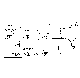
Fig. 1 is a schematic diagram illustrating a light detection and ranging
(LiDAR)
device 100 according to an embodiment of the present disclosure. The LiDAR
device
100 is an example of a range sensor that optically measures the distance. The
LiDAR
device 100 includes a light emitter 1 that emits a laser beam, a light
receiver 2 that
receives the reflected light Lref reflected by an object 40, and a controller
and signal
processor 3 that controls the light emitter 1 and computes the distance based
on the
received reflected light. The light emitter 1 is an example of an optical
device.
[0015] The light emitter 1 includes a laser beam source 11 that is an
example of a light
source, a movable mirror 14 that serves as a scanner, and a projection optical
system
16 that is disposed on the optical path between the laser beam source 11 and
the
movable mirror 14. The projection optical system 16 includes a first optical
element 12
that controls the divergence angle of the laser beam that is emitted from the
laser beam
source 11, and a second optical element 13 that converts the laser beam whose
di-
vergence angle has been controlled into a laser beam with a desired divergence
angle
and angular resolution. The movable mirror 14 scans a desired scanning range 4
with
the laser beam that comes from the second optical element 13 and is incident
on the
movable mirror 14 with a prescribed angular resolution.
[0016] The light receiver 2 includes a light-receiving element 21, an
optical filter 22, and a
condensing optical system 23. The condensing optical system 23 focuses the
retlected
6
CA 03085830 2020-06-15
WO 2019/176360 PCT/JP2019/003638
light Lref reflected by an object 40 on the light-receiving element 21 as
passing
through the optical filter 22. The optical filter 22 is a filter through which
only the
wavelengths near the oscillation wavelength of the laser beam source 11 can
pass
through. The signal-to-noise (SIN) ratio of the light that is incident on the
light-
receiving element 21 improves as wavelengths on both sides of the oscillation
wavelength are cut. The light-receiving element 21 is one or more avalanche
photodiode (APD), and converts the light that has passed through the optical
filter 22
into an electrical signal.
[0017] The controller and signal processor 3 includes a laser beam source
drive circuit 31
that drives the laser beam source 11, a control circuit 32 that controls the
movement (or
deflection angle) of the movable mirror 14, and a signal processing circuit 33
that
computes the distance to the object 40. The laser beam source drive circuit 31
controls
the timing of light emission and light-emission intensity of the laser beam
source 11.
For example, the controller and signal processor 3 is implemented by a large
scale in-
tegration (LS1) chip, an integrated circuit (IC) chip such as a
microprocessor, a logic
device such as a field-programmable gate array (FPGA), and combined use of the
IC
chip and the logic device.
[0018] The light that is emitted from the laser beam source 11 is guided to
the movable
mirror 14 by the first optical element 12 and the second optical element 13,
and the
movable mirror 14 irradiates the object 40 existing in the scanning range 4
with the
scanning light. The reflected light Lref that is reflected by the object 40
passes through
the condensing optical system 23 and the optical filter 22, and is received by
the light-
receiving element 21. The light-receiving element 21 outputs photoelectric
current as a
detection signal, according to the radiation intensity of incident light.
[0019] The signal processing circuit 33 computes the distance to the object
40, which is
calculated from the time difference between a detection signal and a light-
emission
timing signal supplied from the laser beam source drive circuit 31.
[0020] Fig. 2 is a diagram illustrating an example configuration of the
laser beam source 11
according to the present embodiment. For example, the laser beam source 11 in
which
a plurality of laser element groups, each of which is referred to as a layer,
are arranged
on the same plane is composed of a vertical-cavity surface-emitting laser
(VCSEL)
array 11A (surface-emitting laser array). in the following description of the
present
disclosure, a surface-emitting laser element that forms each layer of the
laser beam
source 11 may be referred to simply as a light emitting element. The VCSEL
array
11A includes layers 111-1 to 111-m (that may collectively be referred to as
the layers
1 1 l in the following description), and each of the layers 111 is provided
with a
plurality of light emitting elements 112-1 to 112-n (that may collectively be
referred to
as the light emitting elements 112 where appropriate in the following
description).
7
CA 03085830 2020-06-15
WO 2019/176360 PCT/JP2019/003638
[0021] The light emitting elements 112 are elements that can be integrated
into the same
substrate, and the optical axis of each of the light emitting elements 112 is
orthogonal
to a plane on which the VCSEL array 11A is arranged.
[0022] The timing at which light is emitted from each of the layers 111 is
independently
controlled by the laser beam source drive circuit 31. Moreover, each of the
layers 111
is controlled such that the multiple light emitting elements 112 included in
that layer
111 emit light at the same time.
[0023] In Fig. 2, the multiple layers 111 arc one-dimensionally arranged.
However, no
limitation is indicated thereby, and the VCSEL array 11A in which the multiple
layers
111 are two-dimensionally arranged may be used. The light emitting elements
112 of
each of the layers 111 are minutely arranged with a prescribed pitch with an
ar-
rangement of a honeycomb structure. However, no limitation is intended
thereby. The
shape of the opening of the light emitting elements 112 is also not limited to
a
hexagonal shape. For example, the number of the layers 111 of the VCSEL array
11A,
the number of the light emitting elements 112 in each of the layers 111, and
the
dimension or size of the light-emitting area are designed as desired according
to, for
example, the angular resolution, the scanning range, and the detection
distance that are
required for the LiDAR device 100.
[0024] Fig. 3A and Fig. 3B are diagrams each illustrating the relative
positions of the first
optical element 12 and the VCSEL array 11 A, according to the present
embodiment.
The first optical element 12 is an optical element that controls the
divergence angle of
the laser beam emitted from the VCSEL array 11A. Any desired optical element
array
that can control the divergence angle of the VCSEL array 11A, such as a
microlens
array (MLA) and a diffraction element array, may be adopted as the first
optical
element 12. In the example embodiment as illustrated in Fig. 3A and Fig. 3B, a
MLA
12A is used as the first optical element 12.
[0025] Fig. 3A is a diagram illustrating the VCSEL array 11A and the MLA
12A in an
overlapping manner, in the direction parallel to the optical axis, according
to the
present embodiment. Fig. 3B is a side view of the VCSEL array 11A and the MLA
12A, according to the present embodiment. The MLA 12A includes a plurality of
lens
groups 122 that correspond to the layout of the layers 111 of the VCSEL array
11A.
Each of the lens groups 122 includes a plurality of lens elements 121 as many
as the
light emitting elements 112 of the corresponding layer 111.
[0026] Each of the lens elements 121 is arranged such that the optical axis
matches the
optical axis of the corresponding light emitting element 112, and uses
refraction of
light to control the divergence angle of the laser beam output from each of
the light
emitting elements 112. The lens diameter of the multiple lens elements 121 is
designed
such that the neighboring lens elements 121 do not interfere with each other,
and the
8
CA 03085830 2020-06-15
WO 2019/176360 PCT/JP2019/003638
spacing between the lens elements 121 is narrower than the spacing between the
light
emitting elements 112 of the VCSEL array 11A.
[0027] As illustrated in Fig. 3B, the MLA 12A is arranged on the opposite
side of the
VCSEL array 11A such that the convex surfaces of the lens elements 121 are
placed on
the incident-side of the laser beams output from the VCSEL array 11A. All the
lens
elements 121 of the MLA 12A have the same focal length. The distanced between
the
VCSEL array 11A and the incident plane of the MLA 12A is designed to be equal
to or
shorter than the focal length of the lens elements 121 of the MLA 12A.
[0028] Fig. 4 is a diagram illustrating an example case in which a
diffraction element array
12B is used as the first optical element 12, according to the present
embodiment. The
diffraction element array 12B includes a plurality of lens groups 122 that
correspond to
the layout of the layers 111 of the VCSEL array 11A. Each of the lens groups
122
includes a plurality of diffraction lens 123 as many as the light emitting
elements 112
of the corresponding layer 111.
[0029] The diffraction lens 123 has a concentric cyclic pattern around an
optical axis OA,
and controls the divergence angle of the incident light based on this cyclic
pattern.
Each of the diffraction lenses 123 is arranged such that the optical axis
matches the
optical axis of the corresponding light emitting element 112, and the lens
surface of the
diffraction lens 123 is placed on the incident-side of the laser beams.
[0030] Fig. 5 is a diagram illustrating the relative positions of the
second optical element 13
and the VCSEL array 11A, according to the present embodiment. The second
optical
element 13 is a projector lens that converts the laser beam whose divergence
angle has
been controlled by the MLA 12A into a laser beam with a desired angle of
divergence
and angular resolution.
[0031] "f' denotes the focal length of the projector lens (i.e., the second
optical element 13).
The VCSEL array 11A is arranged at approximately the focal point of the
projector
lens. The angle of divergence of the laser beam 0 and the angular resolution
dO are de-
termined by the focal length f of the projector lens, the size S of the light-
emitting area
of the entirety of the VCSEL array 11A, and the size a of the light-emitting
area of
each of the multiple layers 111, using the First Equation and Second Equation
given
below.
[0032] First Equation
0=2xtan-1[(S/2)/f]
Second Equation
d0=2xtan-1[(a/2)/f]
Fig. 6 is a diagram illustrating optical paths of the projection optical
system 16,
according to the present embodiment. The beam diameters of the laser beams
that have
passed through the projector lens (i.e., the second optical element 13) are
minimized at
9
CA 03085830 2020-06-15
WO 2019/176360 PCT/JP2019/003638
the focal point of the projector lens. The point at which the beam diameter is
minimized is referred to as a beam waist. The beam waist diameter W is
expressed in
the Third Equation using the divergence angle p of the laser beam oscillating
from the
laser beam source and the focal length f of the projector lens.
[0033] Third Equation
W=2fxtan-1(p12)
As understood from the Third Equation as above, the beam waist diameter W can
be
decreased by decreasing the divergence angle p of the laser beam source, and
the light
can be focused on the movable mirror 14 whose area of mirror is small.
[0034] Fig. 7 is a diagram illustrating the MEMS mirror 14A that serves as
the movable
mirror 14. The movable min-or 14 scans the laser beam that has passed through
the
projector lens (i.e., the second optical element 13) in a uniaxial or biaxial
manner and
irradiates the object 40 existing in the scanning range 4 with the scanned
light. The
MEMS mirror 14A is arranged at the beam waist position where the beam diameter
of
the laser beam that has passed through the second optical element 13 is
minimized, i.e.,
approximately the focal point of the second optical element 13.
[0035] The MEMS mirror 14A includes a movable part 144 provided with a
reflection
mirror 145, and a pair of serpentine beams 146 that support the movable part
144 at
both sides of the movable part 144. One end of each one of the serpentine
beams 146 is
fixed to a supporting substrate 143, and the other end of the serpentine beams
146 is
coupled to the movable part 144.
[0036] In each one of the serpentine beams 146, a meandering pattern is
formed as a
plurality of first piezoelectric members 147a and a plurality of second
piezoelectric
members 147b are arranged in alternating sequence having a plurality of
turning
portions between each pair of the first piezoelectric member 147a and the
second
piezoelectric member 147b. An antiphase voltage signal is applied to a
neighboring
pair of the first piezoelectric member 147a and the second piezoelectric
member 147b.
In other words, the phase of the voltage signal that is applied to the first
piezoelectric
member 147a is opposite to the phase of the voltage signal applied to the
second piezo-
electric member 147b. As a result, the serpentine beam 146 is curved in Z-
direction.
[0037] The direction of bending is opposite to each other between a
neighboring pair of the
first piezoelectric member 147a and the second piezoelectric member 147b. The
bending in opposite directions is accumulated, and the movable part 144
provided with
the reflection mirror 145 moves up and down in a rotary motion around a
rotation axis
A. In the example case as illustrated in Fig. 7, the reflection mirror 145 has
a
rectangular shape. However, no limitation is intended thereby. For example,
the re-
flection mirror 145 of an elliptic shape or circular shape may be used.
[0038] A sinusoidal wave that has a drive frequency in view of a mirror
resonant mode
10
CA 03085830 2020-06-15
WO 2019/176360 PCT/JP2019/003638
around the rotation axis A is applied to the first piezoelectric member 147a
and the
second piezoelectric member 147b in opposite phase. As a result, a wide
rotation angle
can be achieved with low voltage.
[0039] Fig. 8 is a diagram illustrating a polygon mirror 14B that serves as
another example
of the movable mirror 14, according to the present embodiment. The polygon
mirror
14B rotates around a rotation axis 141 at a constant velocity. In this
example, plane
mirrors 142a to 142f are disposed on the six inclined planes of a rotor of a
hexagonal
shape. As the rotor rotates on the rotation axis 141, the incident angle of a
laser beam
changes on the mirror surface, and the laser beam can be scanned on the XZ
plane.
[0040] The hades (inclination angles) of the plane mirrors 142a to 142f
with reference to the
rotation axis 141 are different from each other. As a prescribed hade
(inclination angle)
is given to each of the plane mirrors 142a to 142f, the exit angle of a
projector beam in
the Y-axis direction is controlled. Every time the mirror surface where the
laser beam
is reflected is changed, the angle at which the laser beam is output in the Y-
axis
direction changes. The scanning area in the Y-axis direction can be broadened
according to the number of the mirror surfaces that the polygon mirror 14B
has.
First Example
[0041] Fig. 9 is a diagram illustrating the optical scanning performed by
the light emitter 1,
according to a first example. The VCSEL array 11A with one layer and the
movable
mirror 14 of a uniaxial-scanning type are used in the present example
configuration. A
uniaxial-scanning MEMS mirror 14A1 is used as a movable mirror.
[0042] The laser beam that is emitted from the VCSEL array 11A is prevented
from
diverging by the MLA 12A, and is incident on the projector lens (i.e., the
second
optical element 13). The VCSEL array 11A is arranged near the focal length f
on the
incident side of the second optical element 13. The MEMS mirror 14A1 is
arranged
near the focal length f on the light exiting side of the second optical
element 13. The
laser beam that has passed through the second optical element 13 is focused on
the
uniaxial-scanning MEMS mirror 14A1, and is cast in a direction dependent on
the
angle that the incident laser beam forms with the MEMS mirror 14A1.
[0043] In regard to the main scanning direction, the laser beam is scanned
as the rotation
angle of the MEMS mirror 14A1 is changed (see Fig. 7), and in the scanning
range 4
the position of a projection image 10 sweeps in the main scanning direction.
The
scanning range in the main scanning direction depends on the scanning angle of
the
MEMS mirror 14A1. On the other hand, the scanning range in the sub-scanning
direction is determined by the angle of divergence 0 in the sub-scanning
direction of
the VCSEL array 11A. The angle of divergence 0 using Equation 1 as above is de-
termined based on the size S of the light-emitting area of the VCSEL array 11A
in the
sub-scanning direction, and the focal length f of the projector lens (i.e.,
the second
11
CA 03085830 2020-06-15
WO 2019/176360 PCT/JP2019/003638
optical clement 13).
[0044] The angular resolution d0 of the scanning laser beam in both the
main scanning
direction and the sub-scanning direction is determined by the focal length f
of the
projector lens (i.e., the second optical element 13) and the size a of the
light-emitting
area of each of the multiple layers 111 of the VCSEL array 11A, based on the
Second
Equation as above.
[0045] There is a limit to the extent to which the size of the light-
emitting area of each of the
multiple layers 111 can be reduced. However, the laser beam that is emitted
from the
VCSEL array 11A is prevented from diverging by the MLA 12A. Accordingly, a
laser
beam whose beam waist has been stopped down is incident on the reflection area
148
of the MEMS mirror 14A1. Due to this configuration, the radiation intensity of
light
can be prevented from decreasing, and the laser beams can be scanned in a wide
range
while maintaining a high definition.
[0046] In place of the uniaxial-scanning MEMS mirror 14A1, any desired
mirror such as a
polygon mirror, where the angle of the movable mirror uniaxially changes with
reference to the laser beam, may be used.
Second Example
[0047] Fig. 10 is a diagram illustrating the optical scanning performed by
the light emitter 1,
according to a second example of the present disclosure. More specifically,
Fig. 10 il-
lustrates an example configuration in which the VCSEL array 11A with one layer
and
the movable mirror 14 of a biaxial-scanning type are used. A biaxial-scanning
MEMS
mirror 14A2 is used as a movable mirror. As the MEMS mirror 14A2 rotates on a
principal axis Rmain, the laser beams are scanned in the main scanning
direction. As
the MEMS mirror 14A2 rotates on a conjugate axis Rsub, the laser beams are in
the
sub-scanning direction.
[0048] The laser beam that is emitted from the VCSEL array 11A is prevented
from
diverging by the MLA 12A, and is incident on the projector lens (i.e., the
second
optical element 13). The VCSEL array 11A is arranged near the focal length f
on the
incident side of the second optical element 13. The MEMS mirror 14A2 is
arranged
near the focal length f on the light exiting side of the second optical
element 13. The
laser beam that has passed through the second optical element 13 is incident
on the
biaxial-scanning MEMS mirror 14A2, and is cast in a direction dependent on the
angle
that the incident laser beam forms with the MEMS mirror 14A2.
[0049] The MEMS mirror 14A2 changes its angle in the main scanning
direction and the
sub-scanning direction to scan a laser beam. Within the predetermined scanning
range
4, the projection image 10 repeats a sweep in the main scanning direction and
a shift in
the sub-scanning direction in alternating sequence. The scanning ranges in the
main
scanning direction and the sub-scanning direction depends on the scanning
angle of the
12
CA 03085830 2020-06-15
WO 2019/176360 PCT/JP2019/003638
MEMS mirror 14A2. The angular resolution dO of the scanning laser beam in both
the
main scanning direction and the sub-scanning direction is determined by the
focal
length f of the projector lens (i.e., the second optical element 13) and the
size a of the
light-emitting area of each of the multiple layers 111 of the VCSEL array 11A,
based
on the Second Equation as above.
[0050] Also in such an example configuration as above, the laser beam that
is emitted from
the VCSEL array 11A is prevented from diverging by the MLA 12A. Accordingly, a
laser beam whose beam waist has been stopped down is incident on the
reflection area
148 of the MEMS mirror 14A2. Due to this configuration, the radiation
intensity of
light can be prevented from decreasing, and the laser beams can be scanned in
a wide
range while maintaining a high definition.
[0051] In place of the biaxial-scanning MEMS mirror 14A2, any desired
mirror such as a
polygon mirror, where the angle of the movable mirror biaxially changes with
reference to the laser beam, may be used.
Third Example
[0052] Fig. 11 is a diagram illustrating the optical scanning performed by
the light emitter 1,
according to a third example of the present disclosure. In the present
example, the
VCSEL array 11A that include at least two layers 111 in the sub-scanning
direction
and a uniaxial-scanning MEMS mirror 14A1 are used.
[0053] The laser beam that is emitted from the VCSEL array 11A is prevented
from
diverging by the MLA 12A, and is incident on the projector lens (i.e., the
second
optical element 13). The VCSEL array 11A is arranged near the focal length f
on the
incident side of the second optical element 13. The MEMS mirror 14A1 is
arranged
near the focal length f on the light exiting side of the second optical
element 13.
[0054] The timing of light emission of the layers 111-1 to 111-4 of the
VCSEL array 11A is
controlled on an individual basis, and the layers 111-1 to 111-4 of the VCSEL
array
11A are driven in sequence. The laser beams that are emitted from the layers
111-1 to
111-4 are prevented from diverging by the corresponding lens group 122-1 to
122-4 of
the MLA 12A, and are incident on the projector lens (i.e., the second optical
element
13). The positions 131-1 to 131-4 at which the laser beams are incident on the
second
optical element 13 vary in the sub-scanning direction depending on the layer
111 that
is being driven. The laser beam that has passed through the second optical
element 13
is focused by the corresponding one of reflection areas 148-1 to 148-4 of the
uniaxial-
scanning MEMS mirror 14A1, and is cast in a direction dependent on the angle
that the
incident laser beam forms with the MEMS mirror 14A1.
[0055] When the layer 111-1 is being driven, a projection image 10-1 sweeps
in the main
scanning direction at the first position in the sub-scanning direction. When
the layer
111-2 is being driven, a projection image 10-2 sweeps in the main scanning
direction
13
CA 03085830 2020-06-15
WO 2019/176360 PCT/JP2019/003638
at the second position in the sub-scanning direction. When the layer 111-3 is
being
driven, a projection image 10-3 sweeps in the main scanning direction at the
third
position in the sub-scanning direction. When the layer 111-4 is being driven,
a
projection image 10-4 sweeps in the main scanning direction at the fourth
position in
the sub-scanning direction.
[0056] In a similar manner to the first example as above, the scanning
range in the main
scanning direction depends on the scanning angle of the MEMS mirror 14A1. On
the
other hand, the scanning range in the sub-scanning direction is determined by
the angle
of divergence 0 in the sub-scanning direction of the VCSEL array 11A, i.e.,
the size S
of the light-emitting area of the entirety of the VCSEL array 11A, and the
focal length
f of the projector lens (i.e., the second optical element 13), using the First
Equation as
above.
[0057] The angular resolution dO of the scanning laser beam in both the
main scanning
direction and the sub-scanning direction is determined by the focal length f
of the
projector lens (i.e., the second optical element 13) and the size a of the
light-emitting
area of each of the multiple layers 111 of the VCSEL array 11A, based on the
Second
Equation as above.
[0058] In Fig. 11, a plurality of layers 111-1 to 111-4 do not output laser
beams at the same
time. Instead, the timing of light emission is controlled for each one of the
layers 111.
As a result, measurement is performed independently in the four scanning areas
divided in the sub-scanning direction.
[0059] There is a limit to the extent to which the size of the light-
emitting area of each of the
multiple layers 111 can be reduced. However, the laser beams that are emitted
from the
corresponding one of the layers 111 are prevented from diverging by the
multiple lens
groups 122 of the MLA 12A. Accordingly, a laser beam whose beam waist has been
stopped down can be incident on the reflection area 148 of the MEMS mirror
14A1.
Due to this configuration, the radiation intensity of light can be prevented
from de-
creasing, and the laser beams can be scanned in a wide range while maintaining
a high
definition.
[0060] In place of the uniaxial MEMS mirror 14A1, any desired mirror such
as a polygon
mirror, where the angle of the movable mirror uniaxially changes with
reference to the
laser beam, may be used.
Fourth Example
[0061] Fig. 12 is a diagram illustrating the optical scanning performed by
the light emitter 1,
according to a fourth example of the present disclosure. In an example
configuration as
illustrated in Fig. 12, the VCSEL array 11A that include at least two layers
111 in the
sub-scanning direction and the biaxial-scanning MEMS mirror 14A2 are used. The
MEMS mirror 14A2 rotates on a principal axis Rmain to scan the laser beams in
the
14
CA 03085830 2020-06-15
WO 2019/176360 PCT/JP2019/003638
main scanning direction, and rotates on a conjugate axis Rsub to shift the
laser beams
in the sub-scanning direction.
[0062] The laser beam that is emitted from the VCSEL array 11A is prevented
from
diverging by the MLA 12A, and are incident on the projector lens (i.e., the
second
optical element 13), The VCSEL array 11A is arranged near the focal length f
on the
incident side of the second optical element 13. The MEMS mirror 14A1 is
arranged
near the focal length f on the light exiting side of the second optical
element 13.
[0063] In a similar manner to the third example, the timing of light
emission of the layers
111-1 to 111-4 of the VCSEL array 11A is controlled on an individual basis,
and the
layers 111-1 to 111-4 of the VCSEL array 11A are driven in sequence. The laser
beams that are emitted from the layers 111-1 to 111-4 are prevented from
diverging by
the corresponding lens group 122-1 to 122-4 of the MLA 12A, and are incident
on the
corresponding area of the projector lens (i.e., the second optical element
13).
[0064] The laser beam that has passed through the second optical element 13
is concentrated
on the reflection area of the biaxial-scanning MEMS mirror 14A2, and is cast
in a
direction dependent on the angle that the incident laser beam forms with the
MEMS
mirror 14A2. The timing of light emission of the layers 111-1 to 111-4 of the
VCSEL
array 11A is controlled on an individual basis, and the layers 111-1 to 111-4
of the
VCSEL array 11A are driven in sequence. The laser beams that are emitted from
the
layers Ill-Ito 111-4 are prevented from diverging by the corresponding lens
group
122-1 to 122-4 of the MLA 12A, and are incident on the projector lens (i.e.,
the second
optical element 13). The positions 131-1 to 131-4 at which the laser beams are
incident
on the second optical element 13 drive vary in the sub-scanning direction
depending on
the layer 111 that is being driven.
[0065] The laser beam that has passed through the second optical element 13
is concentrated
on one of the corresponding reflection areas 148-1 to 148-4 of the biaxial-
scanning
MEMS mirror 14A2, and is cast in a direction dependent on the angle that the
incident
laser beam forms with the MEMS mirror 14A2.
[0066] When the biaxial-scanning MEMS mirror 14A2 is inclined with
reference to the
conjugate axis Rsub by Osub-n, the projection images that are formed by the
layers
111-1 to 111-4 are referred to as projection images 10-n-1 to 10-n-4,
respectively. In a
similar manner to the third example, when the layer 111-1 is being driven, a
projection
image 10-n-1 sweeps in the main scanning direction at the first position in
the sub-
scanning direction. When the layer 111-2 is being driven, a projection image
10-n-2
sweeps in the main scanning direction at the second position in the sub-
scanning
direction. When the layer 111-3 is being driven, a projection image 10-n-3
sweeps in
the main scanning direction at the third position in the sub-scanning
direction. When
the layer 111-4 is being driven, a projection image 10-n-4 sweeps in the main
scanning
15
CA 03085830 2020-06-15
WO 2019/176360 PCT/JP2019/003638
direction at the fourth position in the sub-scanning direction.
[0067] When the projection images 10-n-1 to 10-n-4 complete a sweep in the
main scanning
direction, the inclination of the biaxial-scanning MEMS mirror 14A2 with
reference to
the conjugate axis Rsub turns to 0sub-(n+1), and a sweep of projection images
10-(n+1)-1 to 10-(n+1)-4 in the main scanning direction is performed in
sequence. By
repeating the above operation, scanning in the sub-scanning direction can be
performed
in a wider range compared with the third example.
[0068] In a similar manner to thc first example, the scanning range in the
main scanning
direction depends on the scanning angle of the MEMS mirror 14A2 in the main
scanning direction. On the other hand, the scanning range in the sub-scanning
direction
is determined by the First Equation and the scanning angle of the MEMS mirror
14A2
in the sub-scanning direction.
[0069] The angular resolution dl) of the scanning laser beam in both the
main scanning
direction and the sub-scanning direction is determined by the focal length f
of the
projector lens (i.e., the second optical element 13) and the size a of the
light-emitting
area of each of the multiple layers 111 of the VCSEL array 11A, based on the
Second
Equation as above.
[0070] In Fig. 12, a plurality of layers 111-1 to 111-4 do not output laser
beams at the same
time. Instead, the timing of light emission is controlled for each one of the
layers 111.
Accordingly, measurement is performed within the scanning range 4
independently in
the four scanning areas divided in the sub-scanning direction.
[0071] There is a limit to the extent to which the size of the light-
emitting area of each of the
multiple layers 111 can be reduced. However, the laser beams that are emitted
from the
multiple layers 111 of the VCSEL array 11A are prevented from diverging by the
multiple lens groups 122 of the MLA 12A. Accordingly, a laser beam whose beam
waist has been stopped down is incident on the corresponding reflection area
148 of
the MEMS mirror 14A2. Due to this configuration, the radiation intensity of
light can
be prevented from decreasing, and the laser beams can be scanned in a wide
range
while maintaining a high definition.
[0072] In place of the biaxial-scanning MEMS mirror 14A2, any desired
mirror such as a
polygon mirror, where the angle of the movable mirror biaxially changes with
reference to the laser beam, may be used.
Fifth Example
[0073] Fig. 13 is a diagram illustrating the optical scanning performed by
the light emitter 1,
according to a fifth example of the present disclosure. In the fifth example,
the VCSEL
array 11A that include at least two layers 111 in the main scanning direction
and the
movable mirror 14 of a uniaxial-scanning type or a biaxial-scanning type are
used. In
the present example as illustrated in Fig. 13, the biaxial-scanning MEMS
mirror 14A2
16
CA 03085830 2020-06-15
WO 2019/176360 PCT/JP2019/003638
is used.
[0074] In the first to fourth examples as above, the multiple layers 111
are scanned in a wide
angle by the movable mirror 14. By contrast, in the fifth example, scanning
area is
divided for each of the layers 111.
[0075] The laser beam that is emitted from the VCSEL array 11A is prevented
from
diverging by the MLA 12A, and are incident on the projector lens (i.e., the
second
optical element 13). The VCSEL array 11A is arranged near the focal length f
on the
incident side of the second optical element 13. The MEMS mirror 14A2 is
arranged
near the focal length f on the light exiting side of the second optical
element 13.
[0076] The laser beam that has passed through the second optical element 13
is concentrated
on the corresponding reflection area of the MEMS mirror 14A2, and is cast in a
direction dependent on the angle that the incident laser beam forms with the
MEMS
mirror 14A2.
[0077] Among the multiple layers 111 of the VCSEL array 11A arranged in the
main
scanning direction, the laser beams that are emitted from the layer 111-1 are
incident
on the corresponding area of the second optical element 13, and a projection
image 101
is formed on a scanning area 411. In a similar manner, the laser beams that
are emitted
from a layer 111-k (in the example of Fig. 13, k denotes an integer of 1 to 4)
are
projected onto the corresponding scanning area 41k by the second optical
element 13,
and an optical image 10k is formed.
[0078] As the MEMS mirror 14A2 performs scanning in the main scanning
direction and the
sub-scanning direction, the optical image 10k sweeps the entirety of the
scanning area
41k. The angular resolution d0 in this configuration in both the main scanning
direction and the sub-scanning direction is based on the Second Equation as
above.
The scanning range 4 in the main scanning direction is determined by the
product of
the optical scanning range of the multiple layers 111 due to the scanning
performed by
MEMS mirror 14A2 and the number of layers of the VCSEL array 11A. The scanning
range in the sub-scanning direction is determined by the scanning range of the
layers
111 due to the scanning performed by MEMS mirror 14A2. The scanning range of
the
movable mirror 14 may be changed such that the size of the scanning area 41
varies for
each of the multiple layers 111.
Sixth Example
[0079] Fig. 14 is a diagram illustrating the optical scanning performed by
the light emitter 1,
according to a sixth example of the present disclosure. ln the sixth example,
the
multiple layers 111 of the VCSEL array 11A are two-dimensionally arranged in
the
main scanning direction and the sub-scanning direction, in comparison to the
scanning
in the fifth example as above. For purposes of simplification, the image of
the MLA
12A is omitted in Fig. 14. Moreover, in accordance with the two-dimensional ar-
17
CA 03085830 2020-06-15
WO 2019/176360 PCT/JP2019/003638
rangement of the layers 111, the multiple lens groups 122 of the MLA 12A are
two-
dimensionally arranged in Fig. 14.
[0080] In the present example, each of the layers 1 1 1 of the VCSEL array
11A is referred to
as a layer 111-ij (where each of i and j denotes a natural number). The laser
beams that
are emitted from the layer 111-ij are prevented from diverging by the
corresponding
lens group 122-ij of the MLA 12A, and are incident on the corresponding
reflection
area 148ij of the MEMS minor 14A2 after passing through the second optical
element
13. The optical image 10ij of the laser beams reflected by the MEMS mirror
14A2 is
projected onto a scanning area 41ij.
[0081] As the MEMS mirror 14A2 is scanned in the main scanning direction
and the sub-
scanning direction, the optical image 10ij scans the entirety of the scanning
area 41ij.
The angular resolution de in the present example is based on the Second
Equation as
above in both the main scanning direction and the sub-scanning direction. The
scanning range in both the main scanning direction and the sub-scanning
direction is
determined by the product of the optical scanning range of the layers 111 due
to the
scanning performed by MEMS mirror 14A2 and the number of layers of the VCSEL
array 11A in each of the scanning directions. The scanning range of the
movable
mirror 14 may be changed such that the size of the scanning area 41 varies for
each of
the multiple layers 111.
[0082] Relative Positions of Light Emitting Elements of VCSEL and Lens
Elements
Fig. 15A and Fig. 15B are diagrams each illustrating the intensity
distribution of a
laser beam when the laser beams that are emitted from a light emitting element
112n
are incident not only on the corresponding lens element 121n but also on an
adjacent
microlenses 121(n+1), according to the present embodiment.
[0083] Fig. 15A is a diagram illustrating an intensity distribution at the
beam waist position,
i.e., an intensity distribution on the reflection plane of the movable mirror
14,
according to an embodiment of the present disclosure. The light that is
emitted from
one of the light emitting elements 112 and is incident on the corresponding
lens
element 121 is focused on the center point, and indicates a high beam
intensity. By
contrast, the light that is incident on a lens element existing in a
peripheral area is
focused on a position different from the image forming position of the target
lens
element 121, and forms an image at a position deviating from the center point,
even at
the beam waist position after passing through the second optical element 13.
The light
that is focused on a peripheral area does not only end up as an optical loss
without
striking the movable mirror 14, but also emerges as stray light at a beam-
waist
position.
[0084] Fig. 15B illustrates an intensity distribution of the light that is
cast (reflected) to a
remote point by the movable mirror 14, according to the present embodiment.
The
Is
CA 03085830 2020-06-15
WO 2019/176360 PCT/JP2019/003638
laser beams that are reflected by the movable mirror 14 are cast to a remote
point, and
the shape of the spot is dispersed in the Y-direction. Even when the shape of
the spot is
dispersed, the laser beams that are incident on the movable mirror 14 after
passing
through the corresponding lens element maintain the intensity to a certain
degree. The
stray light that leaks to the area around after passing through a neighboring
lens
element emerges as stray light of the scanning laser beams. The stray light
that is
present in the periphery of the light to be used to measure the distance leads
to
erroneous detection.
In addition to the necessity for the optical axes of the light emitting
elements 112 and
the lens elements 121 to match, it is desired that the light emitting elements
112 and
the lens elements 121 be arranged such that laser beams do not enter
neighboring lens
elements.
[0085] As an example arrangement, the convex surfaces of the lens elements
121 of the
MLA 12A face the side of the light emitting elements 112 such that the
emergence of
stray light is prevented in the present embodiment.
[0086] Fig. 16A, Fig. 16B, and Fig. 16C are diagrams each illustrating the
principle of the
lens arrangement according to the present embodiment.
[0087] When the lens elements 121 are planoconvex lenses, the MLA 12A is a
lens element
array of a plano-convex type in which the multiple lens elements 121 of a
convex
shape are formed on one side. Typically, as illustrated in Fig. 16B, the flat
side of a
planoconvex lens faces the side of the light emitting elements 112 in view of
the
aberration. However, the effective diameter of each of the lens elements 121
is small in
the case of the MLA 12A, and as known in the art, the thickness of a MLA
substrate is
on the order of several hundred micrometers (um) to several millimeters (mm)
(for
example, 100 urn to 10 mm). As illustrated in Fig. 16B, when the flat side of
the
planoconvex lens faces the side of the light emitting elements 112, at the
timing when
the laser beams that are emitted from a light emitting element 112n reach the
convex
surface of the lens element 121n the laser beams are dispersed equal to or
wider than
the diameter of the lens element 121n, and strike a neighboring lens element
121m.
[0088] In order to handle such a situation, in one example embodiment, as
illustrated in Fig.
16A, the convex surfaces of the lens elements 121 face the side of the light
emitting
elements 112. In the case of LiDAR devices, it is satisfactory as long as the
laser
beams can be controlled within a specific scanning range with a prescribed
angular
resolution. Accordingly, the spherical aberration on the imaging plane does
not have to
be controlled in a strict sense. In other words, the operation of the light
emitter 1 is
almost not at all affected even if the flat side of the MLA does not face the
side of the
light emitting elements 112.
[0089] However, when the distance between the light-emitting surface of the
VCSEL and
19
CA 03085830 2020-06-15
WO 2019/176360 PCT/JP2019/003638
the MLA 12A is too long in such a case as above where the convex surfaces of
the lens
elements 121 face the side of the light emitting elements 112, as illustrated
in Fig. 16C,
laser beams enter neighboring lens elements, and stray light emerges. In order
to avoid
such a situation, the convex surfaces of the lens elements 121 are arranged at
distance
where the optical axes of the light emitting elements 112 match the optical
axes of the
lens elements 121 and the laser beams that are emitted from the light emitting
element
112 do not strike the neighboring ones of the lens elements 121.
[0090] Fig. 17A, Fig. 17B, and Fig. 17C arc diagrams each illustrating the
relative positions
of the light emitting elements 112 and the lens elements 121 when the MLA 12C
of a
double-convex type that has lens elements 121n1 and 121n2 on both sides is
used as
the first optical element 12, according to the present embodiment. As the lens
elements
121n1 and 121n2 of convex type are arranged on both sides of the MLA 12C, the
di-
vergence angle can further be controlled compared with a configuration with
convex
lenses on one side. In this configuration, each of the lens element 121n1 on
the
incident side of the MLA 12C and the lens element 121n2 on the light exiting
side of
the MLA 12C is coaxially arranged with the corresponding light emitting
element
112n.
[0091] Fig. 17A is a diagram illustrating the appropriate relative
positions of the light
emitting element 112n and the lens elements 121n1 and 121n2, according to the
present embodiment. The laser beams that are emitted from the light emitting
element
112n are incident on the convex surface of the lens element 121n1 before the
beam
diameter of those laser beams becomes wider than the lens diameter. The
divergence
angle of the incident laser beams is effectively controlled by the lens
element 121n1
and the lens element 121n2.
[0092] Fig. 17B is a diagram illustrating an arrangement in which the
distance between the
light emitting element 112n and the lens element 121n1 on the incident side is
too
short, according to the present embodiment. On the incident side, the laser
beams are
not incident on the neighboring lens element 121. However, at the timing when
the
laser beams reach the convex surface of the lens element 121n2 on the on the
light
exiting side, the beam diameter of those laser beams becomes wider than the
lens
diameter.
[0093] Fig. 17C is a diagram illustrating an arrangement in which the
distance between the
light emitting element 112n and the lens element 121n1 on the incident side is
too
long, according to the present embodiment. However, at the timing when the
laser
beams reach the convex surface of the lens element 121n1 on the on the
incident side,
the beam diameter of those laser beams becomes wider than the lens diameter.
[0094] When the MLA 12C of a double-convex type is used, it is desired to
be configured
such that the laser beams enter only the corresponding one of the lens
elements 121 on
20
CA 03085830 2020-06-15
WO 2019/176360 PCT/JP2019/003638
both the light entering side and the light exiting side. Due to such a
configuration, the
emergence of stray light can be prevented.
[0095] Fig. 18 is a diagram illustrating an example embodiment in which the
convex
surfaces of the lens elements 121 are arranged on the light exiting side of
the MLA
12A. When the MLA substrate is so thin that the laser beams that are emitted
from the
light emitting element 112n do not enter a neighboring lens elements 121m, the
laser
beams enter only the corresponding lens element 121n, and the laser beams exit
through the convex surface of that lens element 121n. In such cases, the
convex
surfaces of the MLA 12A may be arranged on the light exiting side as
illustrated in
Fig. 18. In other words, in such cases as above, the flat side of the MLA 12A
may be
arranged to face the VCSEL array 11A, When the flat side of the MLA 12A faces
the
side of the light emitting elements 112, a VCSEL substrate can be bonded
together
with a MLA substrate as a package at a wafer level. Accordingly, the
productivity may
increase and the cost may be reduced, which is advantageous. The thickness of
the
MLA substrate as illustrated in Fig. 18 is designed as appropriate in view of
the laser
beams emitted from light emitting elements.
[0096] Focal Length of MLA and Distance between VCSEL and MLA
When the first optical element 12 such as the diffraction element array 12B
and the
MLA 12A or 12C is used, the divergence angles of the laser beams output from
the
multiple light emitting elements 112 of the VCSEL array 11 A can efficiently
be
controlled. However, if the light-emitting areas of the light emitting
elements are
increased to achieve high output power, the reducing effect on the divergence
angle,
which is caused by the first optical element 12, may be affected in an imaging
system.
[0097] If the light-emitting areas are increased in the VCSEL array 11A
where the light
emitting elements 112 are arranged at equal distances, the beam diameter of
the laser
beams increases. In order to prevent the laser beams from entering the
neighboring lens
elements 121 of the MLA 12A, the distance between the VCSEL array 11A and the
MLA 12A needs to be shortened. On the other hand, in the imaging system, the
focal
length of the MLA is shortened, and the divergence angle increases.
[0098] In order to handle such a situation, in the present embodiment, the
first optical
element 12 whose focal length is equal to or longer than the distance d
between the
laser beam source 11 (that is composed of, for example, the VCSEL array 11A)
and
the first optical element 12 (for example, the MLA 12A) is used to achieve the
reducing effect on the divergence angle.
[0099] When the focal length fMLA of the MLA 12A is made longer than the
distance d to
the VCSEL array 11A, the laser beams are deflected by a surface with reduced
curvature (large radius of curvature) compared with curvature with which the
laser
beams are oriented in a parallel direction under ordinary circumstances.
Accordingly,
21
CA 03085830 2020-06-15
WO 2019/176360 PCT/JP2019/003638
the refractive power of light from each light-emitting point is weakened. In
other
words, the divergence angle becomes small compared with when the focal length
fMLA of the MLA 12A is controlled to match the distance d between the VCSEL
and
the MLA.
[0100] Fig. 19A and Fig. 19B are diagrams each illustrating an angular
distribution of the
laser beam emitted through a MLA, according to an embodiment of the present
disclosure. Fig. 19A is a diagram illustrating an angular distribution when
the focal
length fMLA of the MLA matches the distance d between the VCSEL and the MLA
(fMLA=d), according to the present embodiment. Fig. 19B is a diagram
illustrating an
angular distribution when the focal length fMLA of the MLA is longer than the
distance d between the VCSEL and the MLA (fMLA>d), according to the present em-
bodiment.
[0101] In both Fig. 19A and Fig. 19B, the incident plane of the MLA 12A is
arranged away
from the laser beam source whose divergence angle is 18.5 degrees by 80
micrometers
(11m) (d=80 jim), the radiance is used as a function of the angle in the
horizontal
direction (H) and the vertical direction (V) to measure the angle.
[0102] The angular distribution in Fig. 19B (fMLA>d) is closer to a normal
distribution than
the distribution in Fig. 19A (fMLA=d), and the divergence angle in Fig. 19B is
smaller
than the divergence angle in Fig. 19A. When laser beams with broad angular dis-
tribution are focused on the same beam diameter, the intensity gets higher at
the center
and the intensity gets lower in the perimeter zone compared with laser beams
whose
angular distribution is narrow (see the distribution profile of Fig. 19B).
[0103] The loss in light quantity at the movable mirror 14 is equivalent to
the loss in light
quantity of the perimeter zone of the laser beams that were not concentrated
on the
movable mirror 14. Accordingly, even if the divergence angles of laser beams
are all
the same, the image of laser beams with broader angular distribution can be
formed on
the movable mirror 14, with a smaller amount of loss in light quantity. As a
result, the
power of the laser beams that are emitted from the LiDAR device increases, and
the
distance to an object at a long distance can be measured.
[0104] When a MLA whose focal length is longer than the distance d between
the VCSEL
and the MLA is used, the loss in light quantity can be reduced in the imaging
optical
system towards the movable mirror 14, and the LiDAR device can measure the
distance with an improved level of performance.
[0105] Fig. 20A and Fig. 20B are diagrams each illustrating the light-
receptive width of the
movable mirror 14 and the beam-waist shape, according to the present
embodiment. In
the LiDAR devices, laser beams are scanned upon varying the angle of the
movable
mirror 14 with reference to the incident laser beam. Regarding the uniaxial
movable
mirror 14, the light-receptive width Deff of the movable mirror 14 is
expressed in an
22
CA 03085830 2020-06-15
WO 2019/176360 PCT/JP2019/003638
equation given below, using the width D of the movable mirror 14 and the
inclination
OMEMS of the movable mirror 14 with reference to the incident laser beam.
Deff=DxcosOMEMS
[0106] As the inclination of the movable mirror 14 increases, the light-
receptive width
becomes shorter. When wide-angle scanning is performed, the radiation
intensity of
the laser beam that is not focused on the movable mirror 14 increases as the
rotation
angle of the movable mirror 14 increases, and the utilization efficiency of
light may be
affected. In the present embodiment, the divergence angle of the laser beams
is
reduced in advance by the first optical element 12, to minimize the loss in
light
quantity even in the wide-angle scanning.
[0107] Fig. 21A and Fig. 21B are diagrams each illustrating the relation
between the di-
vergence angle and the beam diameter of the laser beam source, according to
the
present embodiment. Fig. 21A is a diagram illustrating the beam diameter in
the sub-
scanning direction when laser beams with varying divergence angles are
concentrated
on the projector lens (i.e., the second optical element 13), according to the
present em-
bodiment. The beam diameters obtained when laser beams whose divergence angle
is
18.5 degrees are concentrated by a projector lens whose focal length is 30
millimeters
(mm) are obtained as a function of the distance from the projector lens, and
are plotted
as the square marks as illustrated in Fig. 21A. The beam diameters obtained
when the
laser beams whose divergence angle is controlled to be 10.6 degrees by the MLA
12A
are concentrated by a projector lens whose focal length is 30 millimeters (mm)
are
obtained and plotted as black dots as illustrated in Fig. 21A. The beam
diameters
obtained when the laser beams whose divergence angle is controlled to be 7.8
degrees
by the MLA 12A are concentrated by a projector lens whose focal length is 30
mil-
limeters (mm) are obtained and plotted as triangular marks as illustrated in
Fig. 21A.
[0108] Regardless of the presence or absence of the MLA 12A, the laser
beams form their
beam waists at a position away from the projector lens by 30 mm, which matches
the
focal length of the projector lens. If the divergence angle is further
controlled by the
MLA 12A, the laser beams may be concentrated with an even smaller beam
diameter.
[0109] Fig. 21B is a graph in which beam waist diameters are plotted as a
function of the di-
vergence angle of the laser beam, according to the present embodiment. The
black dots
indicate measured values, and the dotted lines indicate values calculated
based on the
Third Equation as given above. The focal length f of the projector lens in the
Third
Equation is 30 mm.
[0110] The result of calculation matches the actual beam waist diameter,
and the presence or
absence of an MLA does not matter as long as the light-emitting system is
concerned.
The beam waist diameter after passing through the projector lens (i.e., the
second
optical element 13) can be reduced (see the Third Equation as above),
depending on
23
CA 03085830 2020-06-15
WO 2019/176360 PCT/JP2019/003638
the divergence angle of the laser beam after that laser beam is concentrated
by the
projector lens.
[0111] Fig. 22 is a diagram illustrating the utilization efficiency of
light for different
scanning angles when scanning is performed with varying divergence angles,
according to the present embodiment. In a similar manner to Fig. 21A and Fig.
21B, a
laser beam whose divergence angle is 18.5 degrees where no MLA is involved and
laser beams with the divergence angles of 10.6 degrees and 7.8 degrees where a
MLA
is used arc concentrated on the uniaxial-scanning MEMS mirror 14A by a
projector
lens whose focal length is 30 mm, respectively, at the beam waist position.
The size of
the MEMS mirror 14A is 10 mmx14 mm in the horizontal direction and the
vertical
direction. More specifically, Fig. 22 is a diagram illustrating the
utilization efficiency
of light for different scanning angles when the MEMS mirror 14A rotates in the
main
scanning direction within the range of 140 degrees, according to the present
em-
bodiment.
[0112] As described above, as the divergence angle is smaller, the beam
waist diameter W
of the laser beams that are concentrated by the projector lens becomes small.
Ac-
cordingly, the utilization efficiency of light improves when the scanning
angle gets
wider, and distance can be measured in a wide range of angle. For example,
assuming
that the measurable range is an area with utilization efficiency of light of
95% or
greater, the scannable range of angle is increased from 55 to 100 when the
di-
vergence angle is controlled by the MLA from 18.5 to 10.6 . Further, the
scannable
range of angle is increased from 100 to 120 when the divergence angle is
controlled
by the MLA from 10.6 to 7.8 .
[0113] If such reduction in divergence angle as above is to be applied to a
LiDAR device,
the divergence angle of the VCSEL array 11A is controlled by the MLA 12A. As a
result, the light can be concentrated on the movable mirror 14 whose area of
mirror is
small (for example, the length of a rectangular reflection mirror in the
shorter-side
direction is about 1 mm to 20 mm) in an efficient manner, and long distances
can be
measured in a wide range of angle.
[0114] Fig. 23 is a diagram illustrating the relation between the amount of
defocusing of the
projector lens and the angular resolution in the sub-scanning direction of
each di-
vergence angle, according to the present embodiment. The amount of defocusing
of the
projector lens indicates the distance in which the projector lens is moved
from the focal
point along the optical axis. The negative side in the horizontal axis
indicates cases in
which the projector lens is made close to the VCSEL array, and the positive
side in the
horizontal axis indicates cases in which the projector lens is moved away from
the
VCSEL array.
[0115] As a secondary effect achieved by decreasing the divergence angle,
easing of the
24
CA 03085830 2020-06-15
WO 2019/176360 PCT/JP2019/003638
precision of installation of the projector lens is achieved. As understood
from Fig. 23,
as the divergence angle is decreased, variations a in angular resolution are
small when
the projector lens is displaced from the focal length. As the divergence angle
of the
VCSEL array 11A is controlled due to the MLA 12A, variations in the angular
resolution of the projector lens (i.e., the second optical element 13)
decrease, and
easing of the precision of installation of the projector lens is achieved.
[0116] Fig. 24 is a schematic diagram illustrating a mobile object
installed with the LiDAR
device 100. according to the present embodiment. For example, the mobile
object is a
vehicle 501, and the LiDAR device 100 is attached to the upper side of the
front
windshield or the ceiling of the front seat of the vehicle 501. For example,
the LiDAR
device 100 performs optical scanning in the directions of travel of the
vehicle 501 to
receive the light reflected by the object 40 existing in the directions of
travel. By so
doing, the LiDAR device 100 can recognize the object 40. The light emitter 1
of the
LiDAR device 100 performs optical scanning upon controlling the divergence
angle of
the laser beam in advance by the first optical element 12 such as a microlens
array
(MLA). Accordingly, the optical loss at a scanner such as the movable mirror
14 can
be reduced, and the laser beam can be cast to a remote point with a high
angular
resolution.
[0117] Note that the position to which the LiDAR device 100 is attached is
not limited to the
front and upper side of the vehicle 501, but may be attached to a side or on
the rear of
the vehicle 501. In addition to the application to a vehicle. the LiDAR device
100 is
applicable to any mobile object such as a flight vehicle such as an aircraft
and a drone,
and an autonomous mobile object such as a robot. By adopting the configuration
of the
light emitter 1 according to the embodiments of the present disclosure, the
existence
and position of an object can be detected in a wide range.
[0118] The present disclosure can be implemented in any convenient form,
for example
using dedicated hardware, or a mixture of dedicated hardware and software. The
present disclosure may be implemented as computer software implemented by one
or
more networked processing apparatuses. The processing apparatuses can
compromise
any suitably programmed apparatuses such as a general purpose computer,
personal
digital assistant, mobile telephone (such as a WAP or 3G-compliant phone) and
so on.
Since the present disclosure can be implemented as software, each and every
aspect of
the present disclosure thus encompasses computer software implementable on a
pro-
grammable device. The computer software can be provided to the programmable
device using any conventional carrier medium (carrier means). The carrier
medium can
compromise a transient carrier medium such as an electrical, optical,
microwave,
acoustic or radio frequency signal carrying the computer code. An example of
such a
transient medium is a TCP/IP signal carrying computer code over an IP network,
such
86702562
as the Internet. The carrier medium can also comprise a storage medium for
storing
processor readable code such as a floppy disk, hard disk, CD ROM, magnetic
tape
device or solid state memory device.
[0119] Each of the functions of the described embodiments may be
implemented by one
or more processing circuits or circuitry. Processing circuitry includes a
programmed
processor, as a processor includes circuitry. A processing circuit also
includes devices
such as an application specific integrated circuit (ASIC), digital signal
processor
(DSP), field programmable gate array (FPGA), and conventional circuit
components
arranged to perform the recited functions.
[0120] This patent application is based on and claims priority to Japanese
Patent Application
No. 2018-044805, filed on March 12, 2018, in the Japan Patent Office.
Reference Sings List
[0121] 1 Light emitter (optical device)
2 Light receiver
3 Controller and signal processor
11 Laser beam source
11A VCSEL array
111 Layer (laser element group)
112 Light emitting element (surface-emitting laser element)
12 First optical element
12A MLA (optical element array)
12B Diffraction element array (optical element array)
121 Lens element (optical element)
13 Second optical element
14 Movable mirror
100 LiDAR device (range sensor)
501 Vehicle (mobile object)
Date Recue/Date Received 2021-08-05