Note: Descriptions are shown in the official language in which they were submitted.
CA 03086769 2020-06-23
WO 2019/136202 PCT/US2019/012271
SYSTEM AND METHODS FOR ELECTROKINETIC LOADING OF SUB-MICRON-
SCALE REACTION CHAMBERS
RELATED APPLICATION DATA
[0001] This application claims priority to U.S. provisional application No.
62/614,912 filed
January 8, 2018 and titled, "System and Methods for Electrokinetic Sample
Loading," which
is incorporated by reference herein in its entirety.
FIELD OF THE APPLICATION
[0002] The present application relates to integrated devices and related
instruments that can
perform massively-parallel analyses of samples by providing short optical
pulses to tens of
thousands of reaction chambers or more simultaneously and receiving
fluorescent signals
from the reaction chambers for sample analyses. The instruments may be useful
for point-of-
care genetic sequencing and for personalized medicine.
BACKGROUND
[0003] Instruments that are capable of massively-parallel analyses of
biological or chemical
samples are typically limited to laboratory settings because of several
factors that can include
their large size, lack of portability, requirement of a skilled technician to
operate the
instrument, power need, need for a controlled operating environment, and cost.
When a
sample (e.g., DNA) is to be analyzed using such equipment, a common paradigm
is to extract
a specimen at a point of care or in the field, send the specimen to the lab
and wait for results
of the analysis. The wait time for results can range from hours to days.
BRIEF DESCRIPTION OF THE DRAWINGS
[0004] Various aspects and embodiments of the application will be described
with reference
to the following figures. It should be appreciated that the figures are not
necessarily drawn to
scale. Items appearing in multiple figures are indicated by the same reference
number in all
the figures in which they appear.
[0005] FIG. 1-1 is a schematic of a cross-sectional view of an integrated
device, according to
some embodiments.
CA 03086769 2020-06-23
WO 2019/136202
PCT/US2019/012271
-2-
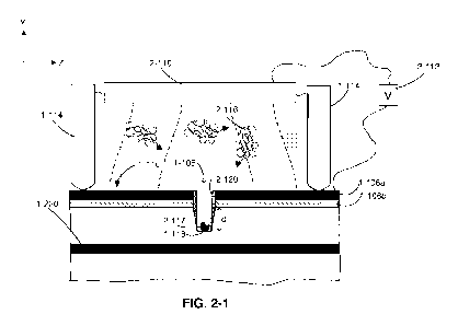
[0006] FIG. 2-1 is a schematic of a cross-section view of an integrated device
having an
electrode configuration for electrokinetic sample loading, according to some
embodiments.
[0007] FIG. 2-2 is a schematic of a cross-section view of an integrated device
having an
electrode configuration for electrokinetic sample loading, according to some
embodiments.
[0008] FIG. 2-3 is a schematic of a cross-section view of an integrated device
having an
electrode configuration for electrokinetic sample loading, according to some
embodiments.
[0009] FIG. 2-4 is a schematic of a cross-section view of an integrated device
having an
electrode configuration for electrokinetic sample loading, according to some
embodiments.
[0010] FIG. 2-5 is a schematic of a cross-section view of an integrated device
having an
electrode configuration for electrokinetic sample loading, according to some
embodiments.
[0011] FIG. 2-6 is a schematic of a cross-section view of an integrated device
having an
electrode configuration for electrokinetic sample loading with contacts to
electrodes formed
as part of the integrated device, according to some embodiments.
[0012] FIG. 2-7 is a schematic of a cross-section view of an integrated device
having an
electrode configuration for electrokinetic sample loading with contacts to
electrodes formed
as part of the integrated device, according to some embodiments.
[0013] FIG. 2-8 is a schematic of a cross-section view of an integrated device
having an
electrode configuration for electrokinetic sample loading with contacts to
electrodes formed
as part of the integrated device, according to some embodiments.
[0014] FIG. 2-9 is a schematic of a cross-section view of an integrated device
having an
electrode configuration for electrokinetic sample loading with vias to
electrodes formed as
part of the integrated device, according to some embodiments.
[0015] FIG. 3-1A is a schematic of a voltage signal applied to electrodes for
electrokinetic
sample loading, according to some embodiments.
[0016] FIG. 3-1B is a schematic of a current waveform provided to electrodes
for
electrokinetic sample loading, according to some embodiments.
[0017] FIG. 3-2 is a schematic of a voltage signal applied to electrodes for
electrokinetic
sample loading, according to some embodiments.
[0018] FIG. 4-1A, FIG. 4-1B, FIG. 4-1C, and FIG. 4-1D depict structures
associated with a
method of forming contacts to an electrically conductive layer(s) of an
integrated device,
according to some embodiments.
CA 03086769 2020-06-23
WO 2019/136202 PCT/US2019/012271
-3-
[0019] FIG. 4-2A, FIG. 4-2B, and FIG. 4-2C depict structures associated with a
method of
forming contact to electrically conductive layer(s) of an integrated device,
according to some
embodiments.
[0020] FIG. 4-3 depicts steps associated with a method of forming vias to an
electrically
conductive layer(s) of an integrated device, according to some embodiments.
[0021] FIG. 4-4A, FIG. 4-4B, and FIG. 4-4C depict structures associated with a
method of
forming a perforated dielectric layer, according to some embodiments.
[0022] FIG. 5-1A is a block diagram of an integrated device and an instrument,
according to
some embodiments.
[0023] FIG. 5-1B is a schematic of an apparatus including an integrated
device, according to
some embodiments.
[0024] FIG. 5-2 is a schematic of a pixel having a reaction chamber, optical
waveguide, and
time-binning photodetector, according to some embodiments.
[0025] FIG. 5-3 is a schematic of an exemplary biological reaction that may
occur within a
reaction chamber, according to some embodiments.
[0026] FIG. 5-4 is a plot of emission probability curves for two different
fluorophores having
different decay characteristics.
[0027] FIG. 5-5 is a plot of time-binning detection of fluorescent emission,
according to
some embodiments.
[0028] FIG. 5-6A is an exemplary time-binning photodetector, according to some
embodiments.
[0029] FIG. 5-6B is an exemplary time-binning photodetector, according to some
embodiments.
[0030] FIG. 5-7A is a schematic illustrating pulsed excitation and time-binned
detection of
fluorescent emission from a reaction chamber, according to some embodiments.
[0031] FIG. 5-7B is a histogram of accumulated fluorescent photon counts in
various time
bins after repeated pulsed excitation of a sample, according to some
embodiments.
[0032] FIG. 5-8A, FIG. 5-8B, FIG. 5-8C, and 5-8D are different histograms that
may
correspond to the four nucleotides (T, A, C, G) or nucleotide analogs,
according to some
embodiments.
CA 03086769 2020-06-23
WO 2019/136202 PCT/US2019/012271
-4-
DETAILED DESCRIPTION
[0033] I. Introduction
[0034] Aspects of the present application relate to integrated devices,
instruments and related
systems capable of analyzing samples in parallel, including identification of
single molecules
and nucleic acid sequencing. Such systems may be compact, easy to carry, and
easy to
operate, allowing a physician or other provider to readily use the system and
transport the
system to a desired location where care may be needed. Analysis of a sample
may include
labeling the sample or associated components (e.g., reaction components) with
one or more
fluorescent markers, which may be used to detect the sample and/or identify
single molecules
of the sample (e.g., individual nucleotide identification as part of nucleic
acid sequencing). A
fluorescent marker may become excited in response to illuminating the
fluorescent marker
with excitation light (e.g., light having a characteristic wavelength that may
excite the
fluorescent marker to an excited state) and, if the fluorescent marker becomes
excited, emit
emission light (e.g., light having a characteristic wavelength emitted by the
fluorescent
marker by returning to a ground state from an excited state). Detection of the
emission light
may allow for identification of the fluorescent marker, and thus, the sample
or a molecule
associated with the sample labeled by the fluorescent marker. According to
some
embodiments, the instrument may be capable of massively-parallel sample
analyses and may
be configured to handle tens of thousands of samples or more simultaneously.
[0035] The inventors have recognized and appreciated that an integrated
device, having
reaction chambers configured to receive the sample and integrated optics
formed on the
integrated device, and an instrument configured to interface with the
integrated device may
be used to achieve analysis of this number of samples. The instrument may
include one or
more excitation light sources, and the integrated device may interface with
the instrument
such that the excitation light is delivered to the reaction chambers using
integrated optical
components (e.g., waveguides, optical couplers, optical splitters) formed on
the integrated
device. The optical components may improve the uniformity of illumination
across the
reaction chambers of the integrated device and may reduce a large number of
external optical
components that might otherwise be needed. Furthermore, the inventors have
recognized and
appreciated that integrating photodetectors on the integrated device may
improve detection
efficiency of fluorescent emissions from the reaction chambers and reduce the
number of
light-collection components that might otherwise be needed.
CA 03086769 2020-06-23
WO 2019/136202 PCT/US2019/012271
-5-
[0036] In the context of single molecule analysis, challenges may arise in
separating a sample
of interest or molecule of interest (e.g., template nucleic acid) from among
other molecules in
a suspension for loading in individual reaction chambers. The inventors have
recognized and
appreciated that isolating a molecule of interest from among other molecules
in a suspension
may be achieved by forming the reaction chambers of the integrated device to
be suitably
sized and shaped to allow for isolation of an individual molecule. In this
manner, a user may
deposit a suspension for analysis on a surface of the integrated device having
an array of the
reaction chambers such that individual reaction chambers may have a high
probability of
receiving a single molecule of the suspension through diffusion. In some
implementations,
the reaction chambers may be suitably sized and shaped such that the
distribution of the
number of molecules that individual reaction chambers receive may allow a
reaction chamber
to receive 0, 1, 2, or more molecules. As an example, the distribution of
molecules of interest
may approximate a Poisson distribution where a fraction (e.g., approximately
35%) of the
reaction chambers receive single molecules.
[0037] In some implementations of the integrated device, a reaction chamber is
positioned
relative to a waveguide such that excitation light propagating through the
waveguide is
coupled to the reaction chamber and illuminates a fluorescent marker used to
label the
molecule. In addition, the reaction chamber is positioned relative to one or
more
photodetectors such that light emitted by the fluorescent molecule is detected
by the
photodetector(s). Challenges may arise in loading molecules into individual
reaction
chambers such that a molecule is positioned within a reaction chamber to allow
for sufficient
excitation of a fluorescent marker and/or sufficient optical detection of
light emitted from a
fluorescent marker. For example, some embodiments of the integrated device
include
reaction chambers that have a bottom surface recessed from a surface of the
integrated device
such that individual reaction chambers have a depth on the order of a hundred
to several
hundred nanometers (e.g., in the range of approximately 100 nm to
approximately 500 nm).
In such embodiments, a molecule and/or a fluorescent marker used to label a
molecule may
need to be positioned proximate to the bottom surface to receive excitation
light and/or for a
photodetector associated with the reaction chamber to receive emission light.
[0038] When using such devices for single molecule analysis, one challenge
that may arise
includes positioning a molecule of interest proximate to the bottom surface of
a reaction
chamber because separating a molecule of interest from a suspension provided
on the surface
of the integrated device may involve moving the molecule of interest from
within the bulk of
CA 03086769 2020-06-23
WO 2019/136202 PCT/US2019/012271
-6-
the suspension and through the depth of the reaction chamber. The efficiency
of loading
molecules into reaction chambers may become diffusion limited due to the
distances that a
molecule may have to move from within the bulk of the suspension to the bottom
surface of a
reaction chamber. For example, the amount of time needed for loading a
molecule into a
reaction chamber increases with the distance of molecule needs to move such
that loading
efficiency may become limited for reaction chambers having large depths. The
amount of
time needed for loading may depend on the size of the molecule such that
larger molecules
may take more time than smaller molecules to move by diffusion from the bulk
of the
suspension to within the reaction chamber. In applications that involve
suspensions having
low molecule concentrations, the low concentration of a molecule of interest
may further
increase the amount of time needed to load the molecules than for suspensions
with high
molecule concentrations. Across an array of reaction chambers, these
limitations that arise
from relying primarily on diffusion for sample loading may impact the ability
to load
molecules within a desired number of reaction chambers in the array such that
only a portion
of the reaction chambers become loaded with a molecule for analysis. The
sample loading
techniques described herein may overcome these limitations by increasing
loading efficiency,
including reducing the time for loading a molecule into a reaction chamber, in
comparison to
relying on diffusion alone. These sample loading techniques may be
particularly suited for
applications that involve loading large molecules, such nucleic acid
molecules, and/or
handling suspensions with particularly low concentrations of molecules. In
applications that
involve nucleic acid molecules, electrokinetic loading may be particularly
beneficial for
molecules containing more than 10,000 bases, 20,000 bases, or 30,000 bases.
Electrokinetic
loading may be particularly beneficial when the concentration of nucleic acid
in a suspension
is less than 100 fM, less than 10 fM, less than 1 fM, or less than 100 pM.
[0039] In particular, the inventors have recognized and appreciated that
applying an electric
field configured to assist loading of a molecule of interest into a reaction
chamber may
improve sample loading efficiency. Such techniques may be considered as
electrokinetic
sample loading because the molecule moves in response to the influence of an
electric field to
a desired location. Using electrokinetic sample loading may involve applying
an electrical
signal to a set of electrodes such that the molecule of interest moves to a
desired location. In
applications where the molecule of interest is charged (e.g., has a net
positive or negative
charge), such techniques may be considered as electrophoretic sample loading
because the
movement of the molecules may depend both on the applied electric field and
the charge of
CA 03086769 2020-06-23
WO 2019/136202 PCT/US2019/012271
-7-
the molecule of interest. In such embodiments, these techniques may be
particularly suited
for transporting a molecule of interest to a desired location because the
electric field may
have a stronger influence on the molecule of interest than for uncharged
molecules.
[0040] Implementing electrokinetic sample loading may involve suitable
positioning of one
or more electrodes configured to generate an electric field, such as in
response to receiving an
electrical signal from circuitry, in the vicinity of a reaction chamber such
that a molecule of
interest moves towards the reaction chamber and/or into the reaction chamber.
The inventors
have recognized and appreciated that the electric field may be generated using
different
arrangements of one or more electrodes. In particular, the inventors have
further recognized
and appreciated that forming an integrated device to include one or more
electrically
conductive layers configured to act as electrode(s) may provide benefits to
improving sample
loading across an array of reaction chambers than if only external electrodes
were
implemented. Incorporating an electrically conductive layer that acts as an
electrode in an
integrated device may allow for improved manipulation of an electric field
(e.g., electric field
strength, directionality) than by using external electrodes alone. In
particular, such an
implementation may allow for generation of an electric field that more
specifically targets
moving molecules from the bulk of a suspension towards and/or into individual
reaction
chambers than through utilization of external electrodes. As an example, the
electrically
conductive layer(s) of an integrated device may act to generate an electric
field having a
suitably high strength at or proximate to a surface of the integrated device
and/or a bottom
surface of a reaction chamber (e.g., a surface recessed from a surface of the
integrated
device), which may improve loading of a molecule. As another example, an
integrated
device may include electrically conductive layer(s) that act as electrode(s)
for individual
reaction chambers of the integrated device such that the electric field for
different reaction
chambers may be individually controlled. As yet another example, an integrated
device may
include electrically conductive layers where one set of layers are configured
to move a
molecule of interest from within the bulk of the suspension towards the
reaction chambers
and another set of layers are configured to move the molecule of interest into
the reaction
chamber. In some instances, the generated electric field may move the molecule
of interest
from within the bulk of a suspension (e.g., in a reservoir positioned over the
integrated
device) towards a reaction chamber.
[0041] In addition, incorporating electrically conductive layer(s) into an
integrated device for
the purpose of electrokinetic sample loading may provide the benefit of
improving the
CA 03086769 2020-06-23
WO 2019/136202 PCT/US2019/012271
-8-
feasibility of implementing an electrokinetic process as part of loading the
sample during use
because it reduces, and in some instances removes, the step of positioning an
electrode
external to the integrated device as part of loading a sample. Instead, a user
may simply
deposit a suspension on a surface of the integrated device and operate
circuitry coupled to the
electrically conductive layer(s) to control generation of an electric field.
In some cases,
operation of the circuitry may be automated (e.g., initiate automatically
after loading a chip
into an instrument and terminate automatically in response to feedback signals
from the chip).
Such a process may improve the amount of time associated with sample loading
and
performing analysis of a sample. In addition, such implementations may improve
the user's
overall experience with using the integrated device and associated instrument
to conduct the
analysis by simplifying the sample loading process.
[0042] According to the techniques described herein, different configurations
of one or more
electrically conductive layers of an integrated device may be used to provide
one or more of
these benefits. In some embodiments of the integrated device, electrically
conductive layer(s)
formed in an integrated device may be formed at or proximate to a surface of
the integrated
device. In some embodiments of the integrated device, some or all of the
reaction chambers
may be formed through the electrically conductive layer(s) of the integrated
device such that
individual reaction chambers form openings or discontinuities within the
electrically
conductive layer(s). In some embodiments, a reaction chamber of an integrated
device may
be separated from an electrically conductive layer of the integrated device by
dielectric
material. In some embodiments, an integrated device may include a circuit,
such as a circuit
coupled to and configured to control a photodetector, formed of the
electrically conductive
layer(s) that are also configured to generate an electric field to assist with
electrokinetic
sample loading, thereby serving a dual purpose for an integrated circuit or
integrated device
and for electrokinetic sample loading. In some configurations, an electric
field that assists
with sample loading may be generated by using the electrically conductive
layer(s) in the
integrated circuit or integrated device as one electrode and another electrode
that is separate
from the integrated device.
[0043] In some embodiments, electrically conductive layer(s) of an integrated
device may be
configured to form both a first electrode and a second electrode used to
assist loading a
molecule into one or more reaction chambers of the integrated device.
Dielectric material
may be formed in the integrated device to electrically isolate the first and
second electrodes
to generate an electric filed, but limit current flow, between the first and
second electrodes.
CA 03086769 2020-06-23
WO 2019/136202 PCT/US2019/012271
-9-
In some embodiments, the same set of electrically conductive layer(s) within
the integrated
device may be used to form both the first electrode and the second electrode.
In such
embodiments, the first electrode and the second electrode may be positioned
relative to the
reaction chamber to generate an electric field laterally over the reaction
chamber. In some
embodiments, a first electrically conductive layer may form a first electrode
and a second
electrically conductive layer may form a second electrode where the first and
the second
electrically conductive layers are separated by dielectric material. In some
embodiments, one
or more sidewalls of reaction chamber may be electrically conductive and
electrically
coupled to one or more electrically conductive layers of the integrated
device. The
electrically conductive sidewall(s) may allow for generation of an electric
field within the
reaction chamber that acts to assist a molecule to move within the reaction
chamber, and in
some instances towards a bottom surface of the reaction chamber.
[0044] To provide electrical signals to the electrically conductive layer(s)
of an integrated
device, an apparatus according to the techniques described herein may include
circuitry
configured to electrically couple to the electrically conductive layer(s)
where the circuitry is
configured to provide electrical signals to the electrically conductive
layer(s) to generate an
electric field. In some embodiments, some or all of the circuitry may be
external to the
integrated device. In some instances, the integrated device may be configured
to interface
with the circuitry such that the circuitry may be electrically coupled through
one or more
electrical connections to assist with sample loading and disconnected or
disabled once a
desired amount of sample loading is achieved. Some embodiments of the
integrated device
may include some or all of the circuitry, such as one or more integrated
circuits formed in the
integrated device and electrically coupled to the electrically conductive
layer(s) of the device.
In some instances, the circuitry may be located both on the integrated device
and external to
the integrated device. Regardless of the configuration of the circuitry, the
circuitry may be
configured to apply a suitable electrical signal to the electrically
conductive layer(s) and/or
external electrode. In some embodiments, the circuitry may be configured to
generate a time-
varying voltage signal and apply the time-varying voltage signal to the
electrically conductive
layer(s). Applying the time-varying voltage signal may generate an electric
field that varies
over time, which may assist with loading of a molecule. A molecule moving
under the
influence of an electric field may have reduced movement or become immobilized
due to a
volume that the molecule occupies in the suspension and how the volume
constrains the
ability of the molecule to move towards and/or into a reaction chambers.
Applying a time-
CA 03086769 2020-06-23
WO 2019/136202 PCT/US2019/012271
-10-
varying voltage may assist with reducing or preventing immobilization of the
molecule by
allowing the molecule to be under the influence of the different types of
electric fields, which
may allow the molecule to reposition or rearrange itself. For example, having
time during a
sample loading process where a molecule is not primarily under the influence
of an electric
field and diffusion dominates the molecule's movement may allow the molecule
to reposition
or rearrange itself, which may assist with loading the molecule into a
reaction chamber when
a subsequent electric field is generated. In some instances, the circuitry may
be configured to
generate a voltage signal having two or more periodic waves with different
frequencies and
apply the signal to the electrically conductive layer(s).
[0045] Other techniques to assist with sample loading may be used in
combination with the
electrokinetic sample loading techniques described herein. Some techniques may
include
introducing one or more agents to a suspension prior to or after depositing
the suspension on
a surface of an integrated device that act to assist with loading a sample of
interest (e.g., a
molecule of interest) into a reaction chamber of the integrated device. Such
agent(s) may
impact the arrangement of the molecule such that it may be more suitable for
loading into a
reaction chamber. One type of agent is a condensing agent configured to reduce
the volume a
molecule of interest occupies in a suspension, which may be considered the
pervaded volume
of the molecule. By introducing a condensing agent, the molecule may have a
smaller
pervaded volume than if the condensing agent was absent and the molecule may
more readily
load into a reaction chamber because of its smaller pervaded volume. Another
type of agent
is a crowding agent configured to reduce the volume accessible to a molecule
in the
suspension. In some embodiments, a crowding agent may increase the
concentration of a
molecule of interest proximate to a surface of the integrated device by
excluding the molecule
of interest from the bulk of the suspension. Examples of suitable condensing
agents and
crowding agents are described further herein and in U.S. Pat. Application No.
15/847,001,
filed December 19, 2017, titled "LOADING MOLECULES INTO REACTION
CHAMBERS FOR ANALYSIS," which is incorporated by reference in its entirety.
[0046] II. Electrokinetic Sample Loading
[0047] A cross-sectional schematic of integrated device 1-102 illustrating a
row of pixels 1-
112 is shown in FIG. 1-1. Pixels 1-112 are formed in pixel region 1-203 of
integrated device
1-102, where individual pixels 1-112 include a reaction chamber 1-108 and
photodetector
region having one or more photodetectors 1-110. Reaction chambers 1-108 may be
formed
CA 03086769 2020-06-23
WO 2019/136202 PCT/US2019/012271
-11-
through surface 1-116 of integrated device 1-102, and in some embodiments
through
electrically conductive layer(s) 1-106. In some embodiments, electrically
conductive layer(s)
1-106 may form surface 1-116 of integrated device 1-102. In some embodiments,
surface 1-
116 of integrated device 1-102 may include dielectric material. Although not
shown in FIG.
1-1, layer(s) of dielectric material may be formed over electrically
conductive layer(s) 1-106,
forming some or all of surface 1-116. In some embodiments of the integrated
device,
openings within the layer(s) of dielectric material may expose a surface of
electrically
conductive layer(s) 1-106 and a reaction chamber may be formed through the
exposed
surface. The resulting configuration may allow for generation of an electric
field having a
desired electric field strength concentrated proximate to the reaction
chamber.
[0048] As shown in FIG. 1-1, pixel region 1-203 may include a recessed region,
which may
be considered as a trench region. Some embodiments may include sample
reservoir 1-114
positioned around some or all of pixel region 1-203, such as by being
positioned around the
trench region as shown in FIG. 1-1. Sample reservoir 1-114 may form a fluid
seal with
surface 1-116 of integrated device 1-102 such that a suspension containing at
least one
sample of interest and/or other components (e.g., crowding agents, condensing
agents) may
be retained within a region over pixel region 1-203. Although FIG. 1-1 only
shows a cross-
sectional view of sample reservoir 1-114, it should be appreciated that, in
some embodiments,
sample reservoir 1-114 may extend in the dimension perpendicular to the view
shown in FIG.
1-1 so that sample reservoir 1-114 forms an enclosed region surrounding pixel
region 1-203.
In some embodiments, sample reservoir 1-114 may be formed on integrated device
1-102 as
part of a packaging process of integrated device 1-102. In such embodiments, a
user may
simply deposit a suspension for analysis within sample reservoir 1-114 as it
is already
positioned to surround pixel region 1-203. In some embodiments, sample
reservoir 1-114
may be detachably coupled to integrated device 1-102. In such embodiments, a
user may
position sample reservoir 1-114 on integrated device 1-102 and deposit a
suspension
containing at least one sample of interest for analysis within sample
reservoir 1-114 prior to
sample analysis. Although only three pixels 1-112 are shown in FIG. 1-1, it
should be
appreciated that any suitable number of pixels may be positioned within a row
of pixels. In
addition, integrated device 1-102 may have any suitable number of rows of
pixels, forming a
pixel array with an array of reaction chambers formed through surface 1-116 of
integrated
device 1-102. Sample reservoir 1-114 may be suitably sized and shaped to
accommodate any
suitable number of reaction chambers 1-108 formed as part of integrated device
1-102.
CA 03086769 2020-06-23
WO 2019/136202 PCT/US2019/012271
-12-
[0049] As part of loading the sample, molecules of interest may enter reaction
chambers 1-
108 and, in some embodiments, may move towards a bottom surface 1-118
positioned
proximate to waveguide 1-220. In embodiments that include sample reservoir 1-
114, loading
a molecule of interest may include using techniques that move the molecule of
interest from
within the bulk of a suspension deposited within sample reservoir 1-114
towards surface 1-
116 of integrated device 1-102. Excitation light propagating along waveguide 1-
220, such as
along the z-direction shown in FIG. 1-1, may illuminate a molecule of interest
and/or a
fluorescent marker labeling the molecule of interest positioned within
reaction chamber 1-
108 by coupling (e.g., evanescently coupling) a portion of the excitation
light from
waveguide 1-220 to reaction chamber 1-108. In some cases, a bottom of the
reaction
chamber is located within one micron of the waveguide 1-220. The molecule of
interest
and/or the fluorescent marker labeling the molecule of interest may emit
emission light in
response to receiving the excitation light, and photodetector(s) 1-110 in the
same pixel as the
reaction chamber 1-108 may receive the emission light. In some cases, metal
layers 1-240
may comprise circuitry for an integrated device 1-102, for example as control
circuitry for
photodetector(s) 1-110.
[0050] According to the techniques described herein, loading of a sample may
include using
electrokinetic sample loading techniques where the integrated device includes
electrically
conductive layer(s) formed into one or more electrodes configured to generate
an electric
field that operates to assist with loading a molecule of interest, for
example, into a reaction
chamber. In some embodiments, the integrated device may include a substrate
having
electrically conductive layer(s) and reaction chamber(s) of the integrated
device may be
formed in a surface of the substrate. FIG. 2-1 shows a schematic of a region
of integrated
device that includes a single reaction chamber 1-108. Sample reservoir 1-114
is shown
around the reaction chamber, but it should be appreciated that more than one
reaction
chamber may be positioned on surface 1-116 of the integrated device and sample
reservoir 1-
114 may be positioned around the multiple reaction chambers. As shown in FIG.
2-1, a
suspension retained within sample reservoir 1-114 may include molecules of
interest 2-116
(e.g., template nucleic acid). In some embodiments, a molecule of interest 2-
116 may
preferentially bind or otherwise interact with a target 2-117 located at a
bottom surface 1-118
of reaction chamber 1-108. In some embodiments, target 2-117 may include
biotin, and a
molecule of interest may include a region that preferentially binds to biotin,
such as
streptavidin. In embodiments where molecules of interest 2-116 are template
nucleic acids,
CA 03086769 2020-06-23
WO 2019/136202 PCT/US2019/012271
-13-
target 2-117 may include a polymerase, which may be immobilized on bottom
surface 1-118.
The polymerase may interact with a template nucleic acid within the reaction
chamber such
that the template nucleic acid is positioned in proximity to bottom surface 1-
118.
[0051] As shown in FIG. 2-1, an integrated device may include electrically
conductive layers
1-106a and 1-106b where reaction chamber 1-108 is formed through both layers 1-
106a and
1-106b. Electrically conductive layers 1-106a and 1-106b may form one or more
electrodes
and may be configured to generate an electric field that operates to assist
loading molecule of
interest 2-116 into reaction chamber 1-108. One or both of electrically
conductive layers 1-
106a and 1-106b may electrically couple to circuitry 2-112. In the embodiment
shown in
FIG. 2-1, circuitry 2-112 is also configured to electrically couple to an
external electrode 2-
110, which is positioned separate from the integrated device and over surface
1-116 of the
integrated device. As shown in FIG. 2-1, external electrode 2-110 may be
separate from
sample reservoir 1-114. In some embodiments, external electrode 2-110 may be
integrated
with sample reservoir 1-114 such that external electrode 2-110 and sample
reservoir 1-114
are mechanically coupled. In other embodiments, external electrode 2-110 may
be
configured to be removably attached to sample reservoir 1-114 such that a user
operating the
system may attach and detach external electrode 2-110 to an interface of the
sample reservoir
1-114. As shown in FIG. 2-1, external electrode 2-110 is positioned in contact
with the fluid
suspension within sample reservoir 1-114. It should be appreciated that some
applications of
the integrated device may involve a different placement of external electrode
2-110 relative
to the suspension located within sample reservoir 1-114. In some embodiments,
external
electrode 2-110 may be positioned over the suspension such that external
electrode 2-110
does not contact the suspension. In other embodiments, external electrode 2-
110 may be
submerged within the suspension.
[0052] Circuitry 2-112 is configured to apply electrical signal(s) to one or
both of layers 1-
106a and 1-106b and electrode 2-110 to generate the electric field that
assists with loading
molecule of interest 2-116 into reaction chamber 1-108. The electric field
(depicted by the
dashed lines) generated by the configuration shown in FIG. 2-1 may be
configured to move a
molecule of interest 2-116 towards surface 1-116 of the integrated device. The
direction of
the electric field can be controlled by the polarity of the electric signal
applied between the
electrode 2-110 and conductive layer(s) 1-106a, 1-106b. Some configurations
may allow for
an electric field to be generated in the vicinity of reaction chamber 1-108
where the electric
field has a higher strength at surface 1-116 than at a distance distal from
surface 1-116, such
CA 03086769 2020-06-23
WO 2019/136202 PCT/US2019/012271
-14-
as within the bulk of the suspension deposited on surface 1-116. Molecules of
interest 2-116
may move towards a region under the influence of the electric field such that
the
configuration shown in FIG. 2-1 drives electrokinetic movement of molecules
towards
surface 1-116, which may increase the total concentration of molecules at
surface 1-116.
[0053] Circuitry 2-112 may be external to the integrated device, such as an
external
controller configured to provide a voltage signal to electrically conductive
layers 1-106a and
1-106b. In some embodiments, circuitry 2-112 may be integrated as part of the
integrated
device. For example, electrical routing may be formed within the integrated
device to
electrically couple with one or both of layers 1-106a and 1-106b. Any suitable
electrically
conductive material may be used to form electrically conductive layers 1-106a
and 1-106b,
including titanium nitride (TiN), titanium, and aluminum (Al). In some
embodiments,
electrically conductive layer 1-106a, which forms surface 1-116, may include
titanium nitride
(TiN) and electrically conductive layer 1-106b may include aluminum (Al). In
other
embodiments, electrically conductive layer 1-106a may include aluminum (Al)
and
electrically conductive layer 1-106b may include titanium nitride (TiN). In
some
embodiments, an electrically conductive layer positioned proximate to a
waveguide of the
integrated device, such as waveguide 1-220, may act to reflect light
propagating along the
waveguide, which may improve optical properties of the integrated device,
including
increasing the amount of light propagating along the waveguide because light
may be
reflected back towards the waveguide.
[0054] Reaction chamber 1-108 may have any suitable depth. Since having a
conductive
layer, such as a metal layer, proximate to the bottom surface of a reaction
chamber may
impact optical properties of the integrated device, including optical
properties associated with
optical coupling of excitation light to the reaction chamber and with optical
detection of light
emitted from the reaction chamber, the depth of reaction chamber 1-108 may
allow for
desired optical properties of the integrated device. In some instances, an
electrically
conductive layer may act as a reflector for light emitted from the reaction
chamber, which
may improve collection of emission light by a photodetector of the integrated
device. Some
embodiments relate to relative positioning of the bottom surface from one or
more
electrically conductive layers to allow for desired optical properties of the
integrated device.
In some instances, the distance d between bottom surface 1-118 and
electrically conductive
layer(s) 1-106 may be in the range of 100 nm and 700 nm, or any value or range
of values in
that range. In some embodiments, distance d may be less than 400 nm.
CA 03086769 2020-06-23
WO 2019/136202 PCT/US2019/012271
-15-
[0055] In some embodiments, reaction chamber 1-108 may have one or more
sidewalls 2-
120, which may be formed of a suitable spacer material (e.g., titanium oxide
(TiO2)). The
spacer material of sidewalls 2-120 may differ from the bottom surface 1-118 to
prevent or
reduce interaction of a molecule of interest with sidewalls 2-120 in
comparison with the
bottom surface 1-118 such that the molecule of interest preferentially binds
or interacts with
the bottom surface 1-118 over the sidewalls 2-120. Such a configuration may
allow for
selective binding, or other type of interaction, of a molecule of interest
with bottom surface,
which may further assist with suitable loading of a molecule of interest into
a reaction
chamber.
[0056] In some embodiments, one or more sidewalls of a reaction chamber may
include
electrically conductive material(s), where the sidewall(s) are electrically
coupled to the
electrically conductive layer(s) of the integrated device. FIG. 2-2
illustrates a cross-sectional
schematic of an integrated device similar to that shown in FIG. 2-1 having
electrically
conductive sidewall(s) 2-122 of reaction chamber 1-108. Sidewall(s) 2-122 may
electrically
couple to electrically conductive layer(s) 1-106 such that applying electrical
signals to
electrically conductive layer(s) allows sidewall(s) 2-122 to also receive
electrical signals and
participate in generating an electric field. In some embodiments, sidewall(s)
2-122 may
include an electrically conductive material that is also used to form one of
the electrically
conductive layers, such as electrically conductive layer 1-106a, as shown in
FIG. 2-2. Any
suitable electrically conductive material may be used to form electrically
conductive
sidewall(s) 2-122, including titanium nitride (TiN), titanium (Ti), tantalum
(Ta), tantalum
nitride (TaN), and tungsten (W). Using an integrated device having
electrically conductive
sidewall(s) of a reaction chamber may generate an electric field within
reaction chamber 1-
108, and in some embodiments may generate an electric field having a high
strength near the
bottom surface 1-118 of the reaction chamber 1-108. Such a configuration of an
integrated
device may increase movement of a molecule of interest towards the bottom
surface 1-118 of
reaction chamber 1-108.
[0057] Some embodiments relate to an integrated device that includes
electrically conductive
layer(s) 1-106 configured to form multiple electrodes in an integrated device.
In such
embodiments, external circuitry may electrically couple to two or more
electrodes formed in
the integrated device. These types of configurations may be used alone or in
combination
with an external electrode. In some embodiments, electrically conductive
layer(s) may be
configured to form a first electrode and a second electrode, where the first
electrode and the
CA 03086769 2020-06-23
WO 2019/136202 PCT/US2019/012271
-16-
second electrode are configured to receive electrical signal(s) to generate an
electric field for
electrokinetic sample loading. Such configurations may allow for
electrokinetic sample
loading without the use of an external electrode, which may improve ease of
use for a user
performing sample analysis. In embodiments where an external electrode is used
in
combination with a set of electrodes formed from electrically conductive
layer(s), circuitry
electrically coupled to the set of electrodes and to the external electrode
may be configured to
apply different electrical signals between different combinations of the
electrodes, which may
allow for improved loading of molecules into individual reaction chambers.
[0058] According to some embodiments, an integrated device may include
multiple
electrically conductive layers 1-106 configured to form two of more
electrodes. The
electrically conductive layers may be separated by dielectric material, which
may reduce or
prevent electrical current between the layers, allowing for electrical signals
to be applied to
the layers to generate an electrical field. FIG. 2-3 shows an exemplary
configuration where
electrically conductive layers form two electrodes as part of an integrated
device. The
integrated device shown in FIG. 2-3 includes electrically conductive layers 1-
106a, 1-106b,
and 1-106c where dielectric layer 2-308 is between electrically conductive
layers 1-106b and
1-106c. In such a configuration, electrically conductive layers 1-106a and 1-
106b may be
considered to form a first electrode and electrically conductive layer 1-106c
may be
considered to form a second electrode. The two electrodes may be positioned
relative to
reaction chamber 1-108 to generate an electric field in the vicinity of
reaction chamber 1-108
in response to the two electrodes receiving electrical signals from circuitry
2-312. It should
be appreciated that any suitable number of electrically conductive layers may
form two
electrodes as long as there is dielectric material positioned between a first
set of electrically
conductive layers and a second set of electrically conductive layers to form
the first and
second electrodes.
[0059] As shown in FIG. 2-3, reaction chamber 1-108 is formed through
dielectric layer 2-
308 such that dielectric layer 2-308 has an opening that overlaps with
reaction chamber 1-
108. In some embodiments, the reaction chamber 1-108 may have tapered
sidewalls such
that a dimension of the opening of dielectric layer 2-308 forming reaction
chamber 1-108 is
smaller than a dimension of an opening of reaction chamber 1-108. For example,
a cross-
sectional dimension (e.g., along the z-direction as shown in FIG. 2-3) of the
opening of
dielectric layer 2-308 is smaller than a cross-sectional dimension (e.g.,
along the z-direction
as shown in FIG. 2-3) of the opening of reaction chamber 1-108. Examples of
suitable
CA 03086769 2020-06-23
WO 2019/136202 PCT/US2019/012271
-17-
dielectric material used to separate two electrically conductive layers in an
integrated device
includes silicon dioxide (SiO2), titanium dioxide (TiO2), tantalum oxide
(Ta05), hafnium
oxide (Hf02), and aluminum oxide (A1203).
[0060] As shown in FIG. 2-3, reaction chamber 1-108 is formed through
electrically
conductive layers 1-106a, 1-106b, and 1-106c. For an array of reaction
chambers of an
integrated device, individual reaction chambers may be formed through each of
electrically
conductive layers 1-106a, 1-106b, and 1-106c. The depth of reaction chamber 1-
108 in these
embodiments may depend on the relative depths of the electrically conductive
layers. In
some embodiments, distance d is between bottom surface 1-118 of reaction
chamber 1-108
and the electrically conductive layer most proximate to bottom surface 1-118,
which in the
integrated device shown in FIG. 2-3 is electrically conductive layer 1-106c.
In the
embodiment shown in FIG. 2-3, reaction chamber 1-108 has sidewalls 2-120,
which may
include spacer material with limited or no electrical conductivity to prevent
or limit electrical
shorting between layers 1-106a, 1-106b and layer 1-106c.
[0061] In some embodiments, an integrated device may include an array of
electrodes formed
of electrically conductive layer(s) where individual electrodes in the array
correspond to
individual reaction chambers. In such embodiments, a first reaction chamber of
the
integrated device may correspond to a first electrode in the array and a
second reaction
chamber of the integrated device may correspond to a second electrode in the
array. The first
and second electrodes may be separated by dielectric material. Circuitry may
apply electrical
signals to individual electrodes in the array, which may allow for individual
control of
electric fields generated for different reaction chambers. Such a
configuration may improve
loading of molecules into reaction chambers because individual reaction
chambers may be
monitored to determine whether a molecule of interest is loaded for analysis
and, if
necessary, modifying the electrical signals applied to the electrode that
corresponds to the
reaction chamber to assist with sample loading. Additionally, in some cases,
the applied
electrical signals may be turned off, reduced, reversed, or reversed and
reduced after the
reaction chamber has been loaded with a sample.
[0062] FIG. 2-4 illustrates a cross-sectional schematic of an integrated
device where
electrically conductive layers 1-106a and 1-106c are sized and shaped, at
least in part, to form
electrodes that correspond to the depicted reaction chamber 1-108. Circuitry 2-
312 may
electrically couple to electrically conductive layers 1-106a and 1-106c, e.g.,
with
interconnects that are located out of the plane of the drawing, and may be
configured to apply
CA 03086769 2020-06-23
WO 2019/136202 PCT/US2019/012271
-18-
electrical signals to layer 1-106c and layers 1-106a, 1-106b. Although only
one reaction
chamber is shown in FIG. 2-4, it should be appreciated that within an array of
reaction
chambers of an integrated device, regions of electrically conductive layers 1-
106a and/orl-
106c can be patterned and positioned to form electrodes that correspond to
individual
reaction chambers. For example, an electrically conductive layer(s) 1-106a
and/or 1-106c
can be patterned to form an isolated electrode surrounding or partially
surrounding a reaction
chamber. In top view, such an electrode may appear annular. The electrodes
formed by
electrically conductive layer 1-106c may be separated by dielectric material 2-
314. As shown
in FIG. 2-4, the individual reaction chambers may be formed through the
discrete regions of
electrically conductive layer 1-106c. For example, a first reaction chamber in
the array may
be formed through a first region of electrically conductive layer 1-106c and a
second reaction
chamber in the array may be formed through a second region of electrically
conductive layer
1-106c where the first and second regions are separated by dielectric
material. As another
example, FIG. 2-9 shows an integrated device having multiple discrete
electrically
conductive layers 1-106c1 and 1-106c2 where a first reaction chamber is formed
through
layer 1-106c1 and a second reaction chamber is formed through layer 1-106c2.
As shown in
FIG. 2-9, layers 1-106c1 and 1-106c2 are separated by a region of dielectric
material 2-614.
In some embodiments, layers 1-106c1 and 1-106c2 are formed by depositing a
layer of a
suitable electrically conductive material and etching portions of the layer to
form layers 1-
106c1 and 1-106c2.
[0063] In some embodiments, sample loading using the integrated devices shown
in FIG. 2-3
and FIG. 2-4 may include using external electrode 2-110 in addition to the two
electrodes
formed by electrically conductive layers 1-106a, 1-106b, and 1-106c. Circuitry
configured to
apply electrical signals to the electrically conductive layer(s) and the
external electrode may
include first circuitry 2-112 configured to apply electrical signals to the
external electrode
and one of the electrodes formed by electrically conductive layer(s) and
second circuitry 2-
312 configured to apply electrical signals to the two electrodes formed by
electrically
conductive layer(s). As shown in FIG. 2-3 and FIG. 2-4, circuitry 2-112 is
electrically
coupled to external electrode 2-110 and electrically conductive layer(s) 1-
106a, 1-106b, and
circuitry 2-312 is electrically coupled to electrically conductive layer 1-
106c and electrically
conductive layer(s) 1-106a, 1-106b. Example electric field lines are depicted
as dashed lines
in FIG. 2-3 and FIG. 2-4. According to some embodiments, the electrodes can be
patterned
to produce an electric field that has an increased intensity in a first region
within 500 nm, for
CA 03086769 2020-06-23
WO 2019/136202 PCT/US2019/012271
-19-
example, of an opening to the reaction chamber compared to a second region
outside the first
region. In some cases, the first region may have a radius larger or smaller
than 500 nm, for
example, between 100 nm and 2 microns.
[0064] As part of a sample loading process, operation of circuitry may include
circuitry 2-
112 and circuitry 2-312 applying different electrical signals to the
electrodes coupled to
circuitry 2-112 and circuitry 2-312. For example, electrical signals applied
by circuitry 2-112
may assist with moving a molecule of interest towards surface 1-116 of the
integrated device
while electrical signals applied by circuitry 2-312 may assist with moving a
molecule of
interest into reaction chamber 1-108. Electrical signals applied by circuitry
2-112 and
circuitry 2-312 may be applied simultaneously, according to some embodiments.
In some
embodiments, electrokinetic sample loading may proceed by applying electrical
signals using
circuitry 2-112 over a first duration of time and applying electrical signals
using circuitry 2-
312 over a second duration of time subsequent to the first duration of time.
[0065] In some implementations of electrokinetic sample loading, circuitry 2-
112 may apply
a first electrical signal between external electrode 2-110 and electrically
conductive layer(s)
1-106a, 1-106b, and circuitry 2-312 may apply a second electrical signal
different than the
first electrical signal between electrically conductive layer 1-106c and
electrically conductive
layer(s) 1-106a, 1-106b. Circuitry 2-112 and circuitry 2-312 may apply the
first electrical
signal and the second electrical signal simultaneously, according to some
embodiments. In
other embodiments, circuitry 2-112 may apply the first electrical signal over
a first duration
of time and circuitry 2-312 may apply the second electrical signal over a
second duration of
time subsequent to the first duration of time. In this manner, applying the
first electrical
signal may move molecules of interest towards surface 1-116, and the
combination of the
first duration of time and the first electrical signal may allow for a desired
concentration of
molecules proximate to surface 1-116 to be achieved. Subsequent application of
the second
electrical signal may move molecules of interest into reaction chambers, and
the combination
of the second electrical signal and the second duration of time may allow for
a desired
amount of reaction chambers to become loaded with a molecule of interest.
[0066] Some embodiments relate to an integrated device that includes
electrodes formed
from the same set of electrically conductive layer(s), where the electrodes
may be configured
to receive electrical signals and generate an electric field to assist with
loading of a molecule
of interest into a reaction chamber. The electrodes may be formed by etching a
region of the
set of electrically conductive layer(s) to form two or more separate regions
of the set of
CA 03086769 2020-06-23
WO 2019/136202 PCT/US2019/012271
-20-
electrically conductive layers. FIG. 2-5 illustrates a cross-sectional
schematic of an
integrated device where electrically conductive layer(s) 1-106a and 1-106b
form different
electrodes. In particular, region 2-502 of electrically conductive layer(s) 1-
106a and 1-106b
has been etched to form a first electrode 2-520 and a second electrode 2-522.
Circuitry 2-512
may be configured to electrically couple to first electrode 2-520 and second
electrode 2-522,
which may generate an electric field. First electrode 2-520 and second
electrode 2-522 may
be positioned relative to reaction chamber 1-108 to generate an electric field
laterally over
reaction chamber 1-108 upon application of electrical signals from circuitry 2-
512. In such
embodiments of the integrated device, surface 1-116 of the integrated device
may have
multiple electrodes arranged to correspond to one or more reaction chambers of
the integrated
device. Although an external electrode is not shown in FIG. 2-5, some
embodiments may
involve applying electrical signals to an external electrode positioned over
reaction chambers
and one or both of first electrode and 2-520 and second electrode 2-522. In
some cases,
region 2-502 may be etched all or nearly all the way around the reaction
chamber 1-108 to
form an annular shaped electrode.
[0067] Some embodiments relate to using circuitry of the integrated device,
such as control
circuitry associated with photodetectors of the integrated device, as one or
more electrodes
for electrokinetic sample loading. FIG. 2-6 illustrates a cross-section
schematic of an
integrated device where metal layer(s) 1-240 have been formed as part of the
integrated
device (e.g., as part of detection circuity located below the reaction
chambers 1-108). In
some embodiments, at least a portion of the circuitry may be configured to
receive electrical
signals for generating an electric field to assist with electrokinetic sample
loading of
molecules into reaction chambers. For example, prior to or intermittently
during operation of
the detection circuitry, at least some of the metal layer(s) 1-240 can be
biased with a signal
used for sample loading. As shown in FIG. 2-6, metal layer(s) 1-240 formed
within the
integrated device are electrically coupled to photodetectors 1-110 to provide
control signals
to photodetectors 1-110 and/or receive readout signals from photodetectors 1-
110. The
integrated device may include a semiconductor (e.g., complementary metal-oxide-
semiconductor (CMOS)) region 2-640, which may include metal layer(s) 1-240.
Optical
structures of the integrated device, including waveguide 1-220, may be formed
within
dielectric material 2-614 where reaction chamber 1-108 and semiconductor
region 2-640 are
separated by dielectric material 2-614.
CA 03086769 2020-06-23
WO 2019/136202 PCT/US2019/012271
-21-
[0068] Some embodiments relate to techniques for forming contacts with
electrically
conductive layer(s) of an integrated device that act as electrode(s) for
electrokinetic sample
loading. Forming the contacts and electrical connections between the contacts
and
electrically conductive layer(s) of the integrated device may occur as part of
packaging of the
integrated device. A packaging process of the integrated device may include
adhering the
integrated device to a printed circuit board. Conductive contacts on the
package (e.g., printed
circuit board) contact electrode(s) formed as part of the integrated device.
In some
embodiments, the conductive contacts of the package may receive electrical
signals from an
instrument, which may include circuitry configured to generate and apply
electrical signals to
the electrode(s) of the integrated device. In some embodiments, the conductive
contacts of
the package may contact a substrate of the integrated device (e.g.,
semiconductor die), which
may include circuitry configured to generate and apply electrical signals to
the electrode(s) of
the integrated device. Additionally or alternatively, wire bonding may be used
to electrically
couple electrically conductive layer(s) of the integrated device to a part of
a package of the
integrated device and/or a substrate of the integrated device. Some
embodiments may
involve complementary-metal-oxide-semiconductor (CMOS) processing techniques
to form
an access region to electrically connect with an electrically conductive layer
of the integrated
device.
[0069] As shown in FIG. 2-6, semiconductor region 2-640 may be formed on
substrate 2-
602, such as a silicon die substrate. In some embodiments, substrate 2-602 may
be attached
to printed circuit board substrate 2-606 via bonding 2-604 (e.g., adhesive
bonding). Contacts
2-608 and 2-610 may be formed on printed circuit board substrate 2-606. As
shown in FIG.
2-6, contact 2-608 may electrically couple to metal layer(s) 1-240, such as by
wire bonding
contact 2-608 to metal layer(s) 1-240. Contact 2-610 may electrically couple
to electrically
conductive layer 1-106b. As shown in FIG. 2-6, a region of the integrated
device is etched to
form recessed region 2-612 to access metal layer(s) 1-240. Recessed region 2-
612 and wire
bonding to contacts 2-606 and 2-610 may occur as part of the packaging process
of integrated
device.
[0070] In some embodiments, a recessed region to access metal layer(s) may be
formed and
electrically conductive layer(s) may be formed over the recessed region to
electrically
connect a metal layer with the electrically conductive layer(s). The metal
layer may be wire
bonded to a contact, such as a contact on a printed circuit board substrate.
As an example,
FIG. 2-7 illustrates recessed region 2-612 to access metal layer 1-240a and
electrically
CA 03086769 2020-06-23
WO 2019/136202 PCT/US2019/012271
-22-
conductive layer 1-106b formed within recessed region and in contact with
metal layer 1-
240a. Recessed region 2-612 also contacts metal layer 1-240a and can allow for
wire
bonding with contact 2-608 of printed circuit board substrate 2-606.
[0071] In some embodiments, packaging component(s) may be used to form
electrical
connections between electrically conductive layer(s) of integrated device and
metal layer(s)
within a semiconductor region of the integrated device as part of forming an
electrical contact
with electrically conductive layer(s). For example a wire bond may pass over
an electrically
conductive layer and a component of the package may press the wire bond into
contact with
the electrically conductive layer, which may be considered as a "wire bond
bridge." As
shown in FIG. 2-8, package component 2-802 presses wire bond 2-804 into
contact with
electrically conductive layer 1-106a, forming a wire bond bridge. Wire bond 2-
804 is in
electrical contact with metal layer(s) 1-240, forming an electrical connection
to contact 2-
608.
[0072] Some embodiments relate to integrated devices having via structures
electrically
coupling conductive layer(s) in the integrated device to circuitry located
within a
semiconductor region of the integrated device. The circuitry in the integrated
device may be
configured to generate and apply electrical signals to the electrically
conductive layer(s)
through the via structures. FIG. 2-9 shows an exemplary cross-sectional
schematic of an
integrated device having conductive via 2-910 formed to electrically couple
conductive layer
1-106c1 to metal layer 1-240a, which is positioned in semiconductor region 2-
640. Similarly,
via 2-920 is shown in FIG. 2-9 to electrically couple conductive layer 1-106c2
to metal layer
1-240b. For illustrative purposes, waveguide 1-220 is shown with dotted lines
in FIG. 2-9 to
indicate the relative positioning of waveguide 1-220 with other structures of
the integrated
device, but is not included in the plane shown in FIG. 2-9 as conductive vias
2-910 and 2-920
are located away from waveguide 1-220 so they do not intrude upon the
waveguide structure.
Although the electrode configuration shown in FIG. 2-9 is similar to the
configuration shown
in FIG. 2-4 in that there is an electrically conductive layer corresponding to
individual
reaction chambers, it should be appreciated that such via structures may be
implemented to
electrically connect an electrically conductive layer forming an electrode
that may assist with
sample loading across multiple reaction chambers.
[0073] Regardless of the configuration of electrodes used for electrokinetic
sample loading,
the electrical signals generated by circuitry coupled and applied to the
electrodes may have
any suitable parameters (e.g., amplitude, temporal profile, duty cycle,
frequency) for
CA 03086769 2020-06-23
WO 2019/136202 PCT/US2019/012271
-23-
achieving loading of molecules into reaction chambers 1-108. In some
embodiments,
parameters of the applied electrical signals may be selected to achieve a
desired level of
efficiency in loading molecules across an array of reaction chambers. For
example,
parameters of the electrical signals may be selected to reduce the amount of
time needed to
achieve sample loading for a particular number, percentage, or ratio of
reaction chambers in
an array of reaction chambers compared to when the electrical signals are not
applied during
loading of the reaction chambers 1-108. Some embodiments involve circuitry
generating and
applying a time-varying voltage signal to electrically conductive layer(s),
and in some
embodiments, to an external electrode. In some cases, DC or exponentially
decaying signals
may be used.
[0074] FIG. 3-1A depicts an example time-varying voltage signal having a
square waveform
that may be applied to an electrode of a reaction chamber 1-108, according to
some
embodiments. In some embodiments, an applied waveform may have a DC offset,
indicated
by the dashed lines in FIG. 3-1A and FIG. 3-1B. The DC offset can provide an
electric field
near the reaction chamber 1-108 that draws a sample toward the reaction
chamber. FIG. 3-
1B depicts an example current response to the square waveform. Application of
such a time-
varying voltage signal may allow for unidirectional movement of a molecule of
interest
towards a surface of an integrated device, and in some instances, into a
reaction chamber. It
should be appreciated that other types of time-varying electrical signals may
be implemented
for electrokinetic sample loading, including time-varying voltage signals
having a sinusoidal
waveform, a sawtooth waveform, and triangle waveform. A peak voltage of an
applied
waveform may be between 50 millivolts and 5 volts. In some implementations,
improved
performance is obtained when a peak voltage of an applied waveform is between
0.5 volt and
1 volt. A frequency of an applied waveform may be between 0.1 Hz and 10 kHz.
In some
embodiments, the applied voltage and frequency can be within 10% of the end
values in these
ranges.
[0075] In some embodiments, the time-varying voltage signal applied to
electrodes for
electrokinetic sample loading may include a combination of multiple periodic
waves (e.g.,
superposition or multiplication of two or more waveforms). One or more of the
applied
waveforms can include a DC bias in some cases. The time-varying voltage signal
may
include a first periodic wave with a first frequency and a first amplitude in
addition to a
second periodic wave with a second frequency and a second amplitude. The first
and second
frequencies may differ, and in some embodiments, the first frequency is less
than the second
CA 03086769 2020-06-23
WO 2019/136202 PCT/US2019/012271
-24-
frequency. Similarly, the first amplitude and the second amplitude may differ,
and in some
embodiments, the first amplitude is greater than the second amplitude. FIG. 3-
2 depicts a
combination, time-varying voltage signal comprising a first square waveform
having a period
Ti and amplitude Al and a second square waveform having a second period T2 and
amplitude A2. As shown in FIG. 3-2, period Ti is greater than period T2, and
amplitude Al
is greater than amplitude A2. Although combined square waveforms are shown,
any
combination of other waveforms (sinusoidal, triangle, sawtooth, exponential
decay, etc.) may
be used in some embodiments. Further, combined waveforms can be of different
types (e.g.,
square wave and sinusoidal wave).
[0076] According to some implementations, electrodes for all reaction chambers
may be
connected together such that an applied signal produces a corresponding
electric field at all
reaction chambers on an integrated device. In some cases, there may be a
plurality of
electrodes that are isolated from each other for receiving applied signals to
produce electric
fields at the reaction chambers 1-108. In such cases, a first set of
electrodes may create a first
electric field for a first group of reaction chambers, a second set of
electrodes may create a
second electric field for a second group of reaction chambers, and so forth.
In some cases,
different signals may be applied to create different electric fields for the
different groups of
reaction chambers. Alternatively or additionally, signals may be applied at
different times to
load groups of reaction chambers at different times. In some implementations,
biasing
circuitry can be arranged similar to read-out circuitry for photodetector
arrays, so that
electrodes for reaction chambers may be individually addressed to create an
electric field at
each reaction chamber 1-108 (or row of reaction chambers, or column of
reaction chambers)
independently of all other reaction chambers.
[0077] During use of the integrated device for sample analysis, a user may
introduce a
suspension (e.g., pipetting a particular suspension volume) having molecules
of interest
proximate to a surface of the integrated device. For example and referring
again to FIG. 1-1,
a user may deposit the suspension on surface 1-116 and/or within pixel region
1-203 of the
integrated device. The recessed pixel region 1-203 and/or sample reservoir 1-
114 may act to
retain the suspension proximate to the surface, such that the suspension does
not substantially
flow from the pixel region 1-203 where the reaction chambers are located.
Electrokinetic
sample loading, according to the techniques described herein, may be used to
load molecules
of interest from a deposited suspension into individual reaction chambers.
Such techniques
may include applying electrical signal(s) to a first and second electrode to
generate an electric
CA 03086769 2020-06-23
WO 2019/136202 PCT/US2019/012271
-25-
field that operates to assist loading a molecule of interest into a reaction
chamber of the
integrated device. One or both of the first and the second electrodes may
include electrically
conductive layer(s) of the integrated device. The electric field may be
generated in a vicinity
of a surface of the integrated device and configured to move the molecule of
interest in a
direction towards a bottom surface of the reaction chamber. In some
embodiments, the
generated electric field may be configured to separate the molecule of
interest from other
components in the suspension (e.g., sample debris, crowding agents, condensing
agents). In
some embodiments, introducing the suspension on the surface of the integrated
device may
include introducing a crowding agent and/or a condensing agent in combination
with the
sample. Additional details on crowding agents and condensing agents are
described herein
including in Section III below.
[0078] Some embodiments may involve modulating the electrical signal applied
to the
electrodes using information identifying whether molecules have been loaded
into individual
reaction chambers of the integrated device. For example, individual molecules
may be
labeled with one or more fluorescent markers, which may be used for
identifying whether a
molecule is loaded in a reaction chamber by illuminating the reaction chamber
with light that
excites the fluorescent marker(s) and using photodetector(s) corresponding to
the reaction
chamber to detect any light emitted from the reaction chamber, which may
include light
emitted by the fluorescent marker(s), in response to the illuminating the
reaction chamber.
Using this feedback information, individual reaction chambers may be monitored
during
electrokinetic sample loading to determine whether molecules have been loaded
into
individual reaction chambers.
[0079] In some applications, this feedback information may inform when to
change the type
of electrical signal that is applied to the electrodes during the sample
loading process. For
example, an electrical signal used for loading molecules may be applied
initially to the
electrodes to allow for loading of the molecules into individual reaction
chambers and a
different electrical signal may be applied to the electrodes in response to
receiving feedback
information identifying that a desired number of reaction chambers have been
loaded with a
molecule. The electrical signal applied in response to receiving the feedback
information
may be configured to generate an electric field that acts to reduce movement
of molecules
into individual reaction chambers and/or reduce movement of a loaded molecule
out of the
reaction chamber in which it is loaded. Such an electrical signal may be
considered as a
"reverse electrical signal" because it acts to prohibit or reduce further
loading of molecules
CA 03086769 2020-06-23
WO 2019/136202 PCT/US2019/012271
-26-
into reaction chambers. Such techniques may further improve loading of
molecules into
reaction chambers by allowing for active monitoring of the reaction chambers
and modifying
the electrical signals applied to the electrodes to account for this feedback
information.
[0080] In embodiments where an electric signal is applied to electrodes such
that an electric
field is generated for a group of reaction chambers, feedback information may
include
information from monitoring across the group of reaction chambers and may
provide an
indication of a number of reaction chambers in the group that are loaded with
a molecule. In
such embodiments, the reverse electrical signal may be applied to the
electrodes in response
to receiving an indication that the number of reaction chambers in the group
that are loaded
with a molecule is equal to or above a threshold number of reaction chambers
that are loaded
with a molecule.
[0081] In embodiments where electrical signals are applied to electrodes such
that the electric
field associated with individual reaction chambers can be modulated, such as
in the
embodiments of the integrated devices shown in FIG. 2-4, FIG. 2-7, and FIG. 2-
9, feedback
information may include information associated with whether particular
reaction chambers
are loaded with a molecule. In such embodiments, a reverse electrical signal
may be applied
to electrodes associated with individual reaction chambers that have been
identified as being
loaded with a molecule based on the feedback information. In this manner,
different electric
fields may be generated proximate to different reaction chambers such that
reaction chambers
that have yet to be loaded with a molecule have an electric field configured
to assist with
sample loading while those reaction chambers that have been identified as
having a loaded
molecule have an electric field to reduce or prevent additional molecules from
entering the
reaction chamber.
[0082] An aspect of performance of the integrated device may relate to the
diffusion of
components in a suspension in/out of the reaction chamber during operation of
the integrated
device (e.g., during analyses of samples). As an example, a DNA complex that
is retained in
a reaction chamber 1-108 can be quite large (have a large pervaded volume),
and the
replication product is growing in size during a sequencing run. In some cases,
a large DNA
complex may occupy much of the volume of the reaction chamber, and thereby
limit the
diffusion rate of fluorescently-labeled nucleotides to the bottom of the
reaction chamber. A
reduced diffusion rate of the labeled nucleotides can limit the sequencing
speed (and
fluorescent pulse rate) as well as the sequencing read length. To improve the
diffusion rate,
electrical signals may be applied to the electrodes during a sequencing run,
for example, to
CA 03086769 2020-06-23
WO 2019/136202 PCT/US2019/012271
-27-
pull at least one untethered end of the DNA out of the reaction chamber. This
would be done
in a way that is similar to the "reverse electrical signal" described above
except that such a
signal would be applied during sequencing or sample analysis when molecules or
proteins
having large pervaded volumes are retained in reaction chambers. In some
cases, a signal
applied to the electrodes during sample analysis may be pulsed periodically to
pull the sample
at least partly out of the well. Such a signal may be applied to electrodes of
reactions
chambers individually for each chamber, applied to groups of chambers, or
applied to all or
nearly all reaction chambers on a chip.
[0083] Circuitry configured to apply electrical signals to the electrodes used
for
electrokinetic sample loading may apply different types of signals. In some
embodiments,
the circuitry may apply a first electrical signal configured to move a
molecule of interest
towards a surface of the integrated device, and apply a second electrical
signal configured to
move the molecule of interest within the reaction chamber. In some instances,
the first
electrical signal is applied to a first electrode and a second electrode, and
the second electrical
signal is applied to the second electrode and a third electrode.
[0084] As discussed above in connection with the different electrode
configurations, circuitry
may apply electrical signals to any suitable combination of electrodes,
including electrodes
formed of electrically conductive layer(s) as well as external electrodes. In
some
embodiments, circuitry may be configured to apply electrical signals to a
first electrode that
includes a first subset of electrically conductive layer(s) and a second
electrode that includes
a second subset of electrically conductive layer(s) that is separated from the
first subset by
dielectric material. In some embodiments, circuitry may be configured to apply
electrical
signals to a first electrode and a second electrode formed of the same
electrically conductive
layer(s). In such embodiments, the first electrode includes a first region of
the electrically
conductive layer(s) and the second electrode includes a second region of the
electrically
conductive layer(s) where the first and the second regions are separated by
dielectric material.
In some embodiments, circuitry may be configured to apply electrical signals
to a first
electrode that includes electrically conductive layer(s) and a second
electrode external to the
integrated device.
[0085] Fabrication of the electrically conductive layer(s) to be formed as
electrodes of an
integrated device may use any suitable silicon-based fabrication processing
(e.g.,
complementary metal-oxide-semiconductor (CMOS) processing). In embodiments
that
implement a wire bond contact, such as wire bond contact of electrically
conductive layer 1-
CA 03086769 2020-06-23
WO 2019/136202 PCT/US2019/012271
-28-
106b to contact 2-610 shown in FIG. 2-6, fabrication may include formation of
a metal layer
in contact with an electrically conductive layer and exposing the metal layer
to form a wire
bond contact. The metal layer may have a thickness in the range of 100 nm to
800 nm, or any
value or range of values in that range. The thickness of the metal layer may
allow for a
robust contact region for wire bonding or an electrically conductive layer
formed over the
metal layer.
[0086] FIGs. 4-1A through FIG. 4-1D show structures associated with an
exemplary process
for forming a metal layer for a wire bond contact to an electrically
conductive layer used to
form an electrode in an integrated device. The first step shown in FIG. 4-1A
includes
forming a metal layer 4-104 (e.g., aluminum (Al)) over dielectric layer 4-102.
Metal layer 4-
104 may have a thickness in the range of 100 nm to 800 nm, or any value or
range of values
in that range. Although not shown in FIG. 4-1A, some embodiments may involve
forming
one or more adhesion layers (e.g., titanium, titanium nitride) underneath
metal layer 4-104.
The second step shown in FIG. 4-1B includes etching a portion of metal layer 4-
104 into
dielectric layer 4-102, which may form a region of the resulting integrated
device having
reaction chambers, such as pixel region 1-203 shown in FIG. 1-1. The third
step shown in
FIG. 4-1C includes forming electrically conductive layers 4-106a and 4-106b
over etched
metal layer 4-104 and dielectric layer 4-102. In some embodiments,
electrically conductive
layer 4-106b includes aluminum and electrically conductive layer 4-106a
includes titanium
nitride. The fourth step shown in FIG. 4-1D includes etching a portion of
electrically
conductive layer 4-106a over metal layer 4-104 to expose electrically
conductive layer 4-
106b. Etching electrically conductive layer 4-106a, and other etching steps
described herein,
may include using any suitable lithography and etching techniques. For
example, a resist
may be applied and patterned to mask regions that are not etched, and the
resist can be
removed after the etching is completed.
[0087] FIGs. 4-2A through FIG. 4-2C show structures associated with an
exemplary process
for forming contacts to electrically conductive layers that may act as
electrodes in an
integrated device. The first step shown in FIG. 4-2A may occur after etching a
metal layer 4-
104 and dielectric material 4-102, such as shown in FIG. 4-1B, and comprise
forming
electrically conductive layer 4-106c, dielectric layer 4-108, electrically
conductive layer 4-
108b, and electrically conductive layer 4-106a over the etched metal layer 4-
104 and
dielectric material 4-102. The second step shown in FIG. 4-2B includes etching
through
layers 4-106a, 4-106b, 4-108, and 4-106c and dielectric material 4-102 to form
a reaction
CA 03086769 2020-06-23
WO 2019/136202 PCT/US2019/012271
-29-
chamber. This step may also include forming sidewall(s) 4-120 on the sides of
the etched
reaction chamber. The third step shown in FIG. 4-2C includes etching contact
opening 4-110
through layers 4-106a, 4-106b, and 4-108 over metal layer 4-104 to expose
electrically
conductive layer 4-106c. This step may also include etching contact opening 4-
112 through
layer 4-106a to expose electrically conductive layer 4-106b. The resulting
integrated device
may have a configuration similar to that shown in FIG. 2-3. It may be
appreciated that sub-
steps (e.g., resist deposition, patterning, removal, cleaning, additional
etching, etc.) may be
carried out to obtain the structures shown in FIG. 4-1A through FIG. 4-1D,
FIG. 4-2A
through FIG. 4-2C, and FIG. 4-4A through FIG. 4-4C.
[0088] Some embodiments relate to fabrication of one or more via(s) within an
integrated
device to connect electrically one or more conductive layer(s) to one or more
metal layer(s),
which may be formed as part of a semiconductor region. Individual vias may be
formed prior
to formation of the electrically conductive layer(s) that electrically couples
to a via. FIG. 4-3
illustrates steps of an exemplary method 4-300 of forming via(s) during
fabrication of an
integrated device, such as the integrated device shown in FIG. 2-9. In step 4-
310, optical
structure(s) (e.g., waveguides) of the integrated device are formed over a
semiconductor
region of the integrated device. With reference to FIG. 2-9, step 4-310 may
include forming
waveguide(s) 1-220 in dielectric material 2-614 over semiconductor region 2-
640, which
includes metal layers 1-240a and 1-240b. In some embodiments, step 4-310 may
include one
or more steps of chemical-mechanical planarization (CMP) processing to form a
planarized
surface for dielectric material 2-614 (e.g., as the dielectric material 2-614
is built up and
integrated structures formed). In embodiments where the integrated device
includes a
recessed or trench region, such as the recessed region 2-905 within pixel
region 1-203 shown
in FIG. 2-9, the recessed region 2-905 may be formed in step 4-310 after
dielectric deposition
and CMP steps, for example.
[0089] The method 4-300 may can comprise step 4-320, which includes etching
vias through
to access metal layer(s) in the semiconductor region. The etching performed in
step 4-320
may include etching through dielectric material, such as dielectric material 2-
614, and/or
some of the material in semiconductor region 2-640 shown in FIG. 2-9, to form
openings that
access the metal layers. The method 4-300 can further comprise step 4-330,
which includes
forming a conductive via 2-910, 2-920 by filling the etched openings with
electrically
conductive material(s). An example of a suitable material used to fill the
etched openings is
tungsten. Step 4-330 may include any suitable metallization processing
techniques, including
CA 03086769 2020-06-23
WO 2019/136202 PCT/US2019/012271
-30-
chemical vapor deposition (CVD). In some embodiments, chemical-mechanical
planarization (CMP) processing may be used following deposition of the
electrically
conductive material(s) in the etched openings to remove excess metal
deposition and to form
a planarized surface over the waveguide leaving conductive plugs (also
referred to as
conductive vias) filling the etched openings. In some embodiments, lithography
and etching
techniques may be used following deposition of the electrically conductive
material(s) in the
etched openings to remove residual material over the waveguide, which may
otherwise
impact optical performance of the waveguide and/or other optical structures of
the resulting
integrated device.
[0090] The method 4-300 can further comprise step 4-340, which includes
forming the
electrically conductive layer(s) 1-106c1, 1-106c2 on the conductive via(s) 2-
910, 2-920, for
example. The electrically conductive layer(s) may be formed using a suitable
deposition
process, including chemical vapor deposition (CVD). Referring to FIG. 2-9,
electrically
conductive layers 1-106c1 and 1-106c2 may be formed at step 4-340. The method
4-300 can
further comprise step 4-350, which includes forming additional layers,
including electrically
conductive layer(s) 1-106a, 1-106b and dielectric layer(s), over the
electrically conductive
layer(s) formed in step 4-340, and forming reaction chamber(s) through the
deposited layers.
In some cases, the recessed region 2-905 can be etched in one or more
dielectric layers that
have been deposited over electrically conductive layer(s) 1-106a, 1-106b.
Examples of
suitable dielectric materials that may be formed over the electrically
conductive layer(s)
include silicon dioxide (SiO2), titanium dioxide (TiO2), tantalum oxide
(Ta05), hafnium
oxide (Hf02), and aluminum oxide (A1203).
[0091] Referring to FIG. 2-9, dielectric material 2-614 and electrically
conductive layers 1-
106a, 1-106b may be formed over electrically conductive layers 1-106c1 and 1-
106c2.
Forming reaction chamber(s) 1-108 may include a multi-step etch process
through one or
more electrically conductive layers and dielectric layer(s). As shown in FIG.
2-9, reaction
chambers 1-108 are formed through electrically conductive layers 1-106a, 1-
106b, and 1-
106c1, 1-106c2 and into dielectric material 2-614. In some embodiments, step 4-
350 may
include forming spacer material on the sidewall(s) of the reaction chamber(s).
For example,
spacer material on sidewalls 2-120 as shown in FIG. 2-9 may be formed in step
4-350.
[0092] Some embodiments of an integrated device may have a surface 1-116
formed, at least
partially, of dielectric material. In some embodiments, one or more layers of
dielectric
material may be formed over the electrically conductive layer(s) and regions
of the one or
CA 03086769 2020-06-23
WO 2019/136202 PCT/US2019/012271
-31-
more layers may be removed to correspond to positions of individual reaction
chambers. In
this manner, the resulting surface of the integrated device may be considered
to have a
"perforated dielectric layer." Such a configuration of an integrated device
may allow for
generating an electric field having a particularly high electric field
proximate to the reaction
chambers. FIG. 4-4A through FIG. 4-4C show structures associated with an
exemplary
process for forming a perforated dielectric layer. The first step shown in
FIG. 4-4A may
occur after etching a metal layer 4-104 and dielectric material 4-102, such as
shown in FIG.
4-1B, and comprise forming electrically conductive layer 4-106c, electrically
conductive
layer 4-108b, electrically conductive layer 4-106a, and dielectric layer 4-408
over the etched
metal layer 4-104 and dielectric material 4-102. The second step shown in FIG.
4-4B
includes etching through dielectric layer 4-408 in regions to expose
electrically conductive
layer 4-106a. Etching dielectric layer 4-408 may include using any suitable
lithography and
etching techniques. The third step shown in FIG. 4-4C includes etching through
layers 4-
106a, 4-106b, 4-108, and 4-106c to form individual reaction chambers at
locations
corresponding to the exposed regions of electrically conductive layer 4-106a.
This step may
also include forming sidewall(s) 4-120 on the sides of the etched reaction
chamber. Although
only one dielectric layer is shown as dielectric layer 4-408, it should be
appreciated that any
suitable number of layers of dielectric material may be formed over the
electrically
conductive layer(s). Examples of dielectric materials that may be used to form
dielectric
layer 4-408 include silicon dioxide (5i02), titanium dioxide (TiO2), tantalum
oxide (Ta05),
hafnium oxide (Hf02), aluminum oxide (A1203), and other metal oxides.
[0093] III. Additional Sample Loading Techniques
[0094] Among other aspects, the present application describes devices and
methods for
loading a sample of interest into a reaction chamber. In some aspects,
techniques described
herein involve steps of contacting a suspension containing samples (e.g.,
molecules, proteins,
or particles of interest) to a surface 1-116 of an integrated device
comprising at least one
reaction chamber having a bottom surface distal to the surface of the
integrated device. A
suspension may comprise a liquid solution that contains a plurality of samples
that is placed
in recessed region 2-905. In some cases, a suspension may comprise a liquid in
which the
samples are dissolved. In some cases, a suspension may comprise a liquid in
which the
samples are dispersed. The term "suspension" is used herein to refer to either
type of sample
mixture. A suspension can further include reaction components that participate
in a reaction
CA 03086769 2020-06-23
WO 2019/136202 PCT/US2019/012271
-32-
that takes place in a reaction chamber. In some embodiments, the suspension
may be
contacted with a crowding agent that further directs the samples toward the
bottom surface of
the reaction chamber. In some embodiments, the suspension may be contacted
with a
condensing agent that condenses (e.g., compacts) the samples. In some
embodiments, the
bottom surface of the reaction chamber comprises a coupling moiety configured
to bind the
sample of interest, under conditions suitable to permit binding of the sample
to the coupling
moiety, thereby coupling the sample to the bottom surface of the reaction
chamber.
[0095] In some aspects, devices and methods described herein may be useful in
techniques
that allow for the detection of an individual sample in a suspension. The
individual sample
may be, by way of example and not limitation, an amino acid, a polypeptide, a
nucleotide,
and/or a nucleic acid. For example, in some embodiments, devices and methods
provided in
the present application may be used in conjunction with single molecule
nucleic acid
sequencing technologies. Single molecule nucleic acid sequencing allows for
the
determination of a sequence of a single template nucleic acid molecule by
monitoring, in real
time, the extension of a nucleic acid molecule that is complementary to the
template nucleic
acid.
[0096] In certain techniques, single molecule nucleic acid sequencing is
performed by
isolating single sequencing templates within each of a plurality of reaction
chambers. In
many applications, however, the total volume of these reaction chambers
relative to the total
suspension volume is considerably low. Additionally, the concentration of
sequencing
template in a suspension that is required to minimize multiple templates in
single reaction
chambers is often so low that the kinetics of loading the sequencing templates
into the
reaction chambers can severely limit the amount of successfully loaded and
sufficiently
active complexes.
[0097] In certain techniques, it is preferable for a single reaction chamber
to comprise a
single sample of interest (e.g., a single sequencing template). Accordingly,
in some
embodiments, when loading a suspension that comprises, for example, a
sequencing
template, onto an integrated device comprising an array of reaction chambers,
care must be
taken to avoid oversaturating the integrated device with a high concentration
of the
sequencing template. It is often advisable, in such instances, to load
suspensions having a
dilute concentration of sequencing template.
[0098] Without wishing to be bound by theory, it is postulated that the
distribution of
sequencing templates in a suspension of dilute concentration across an array
of reaction
CA 03086769 2020-06-23
WO 2019/136202 PCT/US2019/012271
-33-
chambers is best modeled by a Poisson distribution. This discrete probability
distribution
predicts that approximately 37% of the reaction chambers in an array will
contain one
sequencing template, with the remaining reaction chambers containing either
zero or multiple
sequencing templates. In practice, achieving 37% single occupancy across an
array of
reaction chambers can be complicated by any number of chemical and/or
mechanical
variables. In some aspects, devices and methods described herein
advantageously increase
the percentage of single occupancy across an array of reaction chambers.
[0099] In some embodiments, devices and methods described herein are capable
of achieving
single occupancy of molecules of interest in an array of reaction chambers
that is comparable
to, approximately the same as, or greater than the amount predicted by Poisson
statistics. For
example, in some embodiments, devices and methods of the present disclosure
may achieve
single occupancy of molecules of interest between 20% and 25% of reaction
chambers in an
array, between 25% and 30%, between 30% and 35%, between 35% and 37%, between
37%
and 40%, between 40% and 45%, between 45% and 50%, between 50% and 60%,
between
60% and 70%, between 70% and 80%, between 80% and 90%, between 90% and 95%,
between 95% and 99%, or between 95% and 100% of reaction chambers in an array.
In some
cases, the occupancy may be within 10% of the end values in one or more of
these ranges.
[0100] Devices and methods described herein may allow for loading molecules of
interest
into reaction chambers of extremely small volumes. For example, in some
embodiments, the
capacity of a sample reservoir (e.g., a recessed region 2-905) in an
integrated device and all
reaction chambers therein is approximately 20 x 10-6 L, with each reaction
chamber having a
volume of approximately 3 x 10-18 L. In some embodiments, an integrated device
contains
512,000 reaction chambers. Accordingly, in some embodiments, the total volume
of all
reaction chambers accounts for approximately 0.00000768% of the capacity for a
suspension.
[0101] A. Crowding Agents
[0102] In some embodiments, a crowding agent may effectively exclude samples
of interest
(e.g., sequencing templates) from bulk solvent of a suspension. The inclusion
of a crowding
agent may produce a volume exclusion effect that excludes molecules of
interest from the
bulk volume of a suspension, which can assist in driving the molecules of
interest towards
and/or into reaction chambers. As a result, a greater percentage of reaction
chambers are
capable of receiving a successfully loaded molecule of interest. Thus, in some
embodiments,
crowding agents may produce a thermodynamic driving force that effectively
increases the
concentration of the molecule of interest at the surface of an integrated
device. In some
CA 03086769 2020-06-23
WO 2019/136202 PCT/US2019/012271
-34-
embodiments, crowding agents may decrease loading time by having a kinetic
effect that
accelerates the movement of the molecules of interest into the reaction
chambers.
[0103] As used herein, a "crowding agent" is any compound or molecule that
allows for,
enhances, or facilitates sample crowding. Without wishing to be bound by any
particular
mechanism, it is suggested that crowding agents reduce the volume of solvent
that is
available for samples or other macromolecules. This excluded volume effect
limits the
volume accessible to samples or macromolecules as a result of non-specific
interactions, such
as steric repulsion, with the crowding agent. Accordingly, in some
embodiments, a crowding
agent may be referred to as a "volume excluder" or "volume excluding agent."
In some
embodiments, the crowding agent is inert with respect to other components in
the same
suspension. In some embodiments, the crowding agent does not interfere with
reactions
occurring in the same suspension.
[0104] It should be appreciated that different types of crowding agents that
create a volume
exclusion effect may be used as part of the sample loading techniques
described herein.
Some types of crowding agents may attract water, allowing molecules other than
water to
aggregate and/or become concentrated at a particular location, such as at a
surface of an
integrated device. In some instances, the crowding agent binds to and/or ties
up water in a
suspension to exclude a sample or macromolecule in the suspension. Another
type of
crowding agent may act to compact a volume of a molecule of interest, such as
a sequencing
template, in a suspension. Such crowding agents may allow larger sequencing
templates to
be loaded into the reaction chamber because the overall volume of the
sequencing template is
reduced. Other types of crowding agent may promote phase separation and/or
exert osmotic
pressure.
[0105] Including one or more crowding agents as part of a sample loading
process may
facilitate loading of molecules of interest into reaction chambers, including
facilitating
loading of molecules over longer distances and more faster than if no crowding
agents were
used. In this manner, a crowding agent may decrease the time required to
incubate a
suspension on an integrated device comprising reaction chambers before single
molecule
analysis, for example, of samples using the device can be performed. In some
implementations, a particular crowding agent may be selected such that it
stays (e.g.,
preferentially) in a sample reservoir as opposed to migrating into reaction
chambers. In some
embodiments, this promotes a thermodynamic driving force that drives the
loading of
samples (e.g., DNA-polymerase complex) into the reaction chambers. In some
embodiments,
CA 03086769 2020-06-23
WO 2019/136202 PCT/US2019/012271
-35-
lower viscosity crowding agents such as Ficoll or polyvinylpyrrolidone have
high mobility
and poor localization relative to higher viscosity agents and are not as
effective as the higher
viscosity agents. However, it should be appreciated that lower viscosity
agents may be useful
in some contexts.
[0106] In some embodiments, the crowding agent is a polysaccharide. In some
embodiments, the crowding agent is a cellulose molecule. In some embodiments,
the
crowding agent is methyl cellulose. In some embodiments, the crowding agent is
a cellulose
molecule selected from the group consisting of ethyl cellulose, ethyl methyl
cellulose,
hydroxyethyl cellulose, hydroxypropyl cellulose, hydroxyethyl methyl
cellulose,
hydroxypropyl methyl cellulose, ethyl hydroxyethyl cellulose, carboxymethyl
cellulose, and
derivatives and combinations thereof. In some embodiments, the crowding agent
is a Ficoll
polymer. In some embodiments, a crowding agent, such as a cellulose crowding
agent (e.g.,
Methocel MC of 63,000), has an average molecular weight of 50,000 to 500,000
Da (e.g.,
from 50 kDa to 100 kDa in some embodiments, from 100 kDa to 200 kDa in some
embodiments, from 200 kDa to 300 kDa in some embodiments, from 300 kDa to 400
kDa in
some embodiments, and yet from 400 kDa to 500 kDa in some embodiments). In
some cases,
a crowding agent may have an average molecular weight greater than 500 kDa.
[0107] In some embodiments, the crowding agent is provided in a suspension to
which
samples for analysis may be or have been added. In some embodiments,
concentration of the
crowding agent in the suspension is between 0.6% and 0.9% by weight or equal
to either of
the end values. In some embodiments, concentration of the crowding agent in
the suspension
is between 0.9% and 1.8% by weight or equal to either of the end values. In
some
embodiments, concentration of the crowding agent in the suspension is between
1.8% and
2.0% by weight or equal to either of the end values. In some embodiments,
concentration of
the crowding agent in the suspension is between 2.0% and 2.3% by weight or
equal to either
of the end values. In some embodiments, concentration of the crowding agent in
the
suspension is about 2.3% by weight. In some embodiments, the crowding agent is
present in
the suspension between 0.1% by weight to 1.0% by weight, between 1.0% by
weight to 5.0%
by weight in some cases, between 5.0% by weight to 10.0% by weight in some
cases, and yet
between 10.0% by weight to 20.0% by weight in some cases. In some
implementations, the
concentration of the crowding agent in the suspension may have a greater value
than 20% by
weight. In some cases, the concentration of the crowding agent is within 10%
of the
expressed ranges or values above.
CA 03086769 2020-06-23
WO 2019/136202 PCT/US2019/012271
-36-
[0108] In some embodiments, a crowding agent is provided in the form of a gel
(e.g., a
hydrophilic gel) that can be placed in direct contact with a suspension (e.g.,
in a sample
reservoir). Gels can be applied (e.g., in the form of a gel plug) without
being limited by
pipetting considerations and higher concentrations and viscosities of crowding
agent can be
used in the form of a gel. In some embodiments, the crowding agent is provided
in a solid
state. For example, in some embodiments, the crowding agent is provided as a
film, a fibrous
material, a membranous material, an adhesive material, a composite material, a
laminate
material, or some combination thereof.
[0109] B. Condensing Agents
[0110] As used herein, "condensing agent" refers to any natural or synthetic
compound,
which when combined with a sample of interest causes the sample of interest
(e.g., a
molecule or macromolecule) to assume a condensed structure relative to its
structure in
absence of the condensing agent. For example, in a given suspension, the
sample of interest
occupies a smaller volume in the presence of the condensing agent than the
same suspension
lacking the condensing agent. In this manner, a condensing agent may act to
reduce the
occupancy volume of the sample of interest (e.g., a molecule) in the
suspension. In the
context of a molecule in a suspension, a condensing agent may act to reduce
the pervaded
volume of the molecule of interest in the suspension. The condensing agent may
interact
with the molecule of interest such that the molecule adopts a compacted
structure that
occupies a smaller fraction of the total volume in a suspension.
[0111] In some embodiments, the condensing agent is a nucleic acid condensing
agent.
Nucleic acid condensing agents can compact nucleic acids by a variety of
mechanisms,
including, but not limited to, volume exclusion and charge screening. Assays
to evaluate the
capability of an agent to condense nucleic acids are known in the art, e.g.,
as described in
WO/1996/021036, the relevant content of which is incorporated herein by
reference in its
entirety. In some embodiments, a nucleic acid condensing agent interacts with
nucleic acids
via electrostatic charge-charge interactions to induce a collapsing of the
nucleic acid structure
(e.g., nucleic acid condensation). In some embodiments, a condensing agent can
condense a
nucleic acid as a result of one or more of the following: exerting osmotic
pressure to bring
segments of the helical structure together (e.g., molecular crowding effect),
decreasing
repulsive interactions between nucleic acid segments (e.g., by neutralizing
phosphate charge),
and increasing attractive interactions between nucleic acid segments. In some
embodiments,
CA 03086769 2020-06-23
WO 2019/136202 PCT/US2019/012271
-37-
attractive interactions between the DNA segments can be induced by multivalent
cationic
charged condensing agents.
[0112] In some embodiments, a condensing agent comprises a polycation. As used
herein, a
polycation refers generally to a compound having a plurality of positively
charged sites. In
some embodiments, the polycation is polycationic when present in a suspension
that includes
a molecule of interest. For example, in some embodiments, conditions (e.g.,
pH, buffer
capacity, ionic strength) in a suspension comprising a molecule of interest
are such that the
condensing agent is polycationic in the suspension. In some embodiments, the
polycation is
polycationic at physiological pH (e.g., pH ,-=,' 7.4). In some embodiments,
the polycation is a
polymer of positively charged monomeric units, although some non-positively
charged units
may be present in the polymer. Examples of polycations include, in some
embodiments,
polyamines, such as spermine, spermidine, and putrescine. In some embodiments,
the
polycation comprises a polyamino acid, such as polyhistidine, polylysine,
polyarginine, and
polyornithine. Other basic peptides and small basic proteins are further
contemplated for use
as polycationic condensing agents (e.g., histones, protamines). For
polycations composed of
amino acids, either the L- or D- forms may be used. Basic amino acids include
lysine,
arginine, amino acid analogues such as ornithine and canaline, modified basic
amino acids,
such as homoarginine, and other modified amino acids modified to carry a
positive charge,
such as guanidinovalinate, and aminoethylcysteine. Additional examples of
polycations
include polyammoniums (e.g., Polybrene (hexadimethrine bromide)), lipids
(e.g., DOTAP,
DC-Chol/DOPE, DOGS/DOPE, and DOTMA/DOPE).
[0113] C. Loading Suspensions on Integrated Devices
[0114] In some aspects, the present application provides devices and methods
useful for
loading a suspension comprising at least one sample of interest onto a surface
of an integrated
device 1-102 that includes reaction chambers 1-108. Suspension loading may be
conducted
by any number of suitable methods. In some embodiments, the suspension
containing
molecules of interest, for example, is loaded by a practitioner, e.g., via a
pipette, a dispenser,
or any suitable fluid transfer device/system. In some embodiments, the
suspension is loaded
by automated means (e.g., a robotic device/system). In some embodiments, the
suspension is
loaded via one or more microfluidic channels.
[0115] In some embodiments, a sample of interest can be delivered to an
integrated device
(e.g., an integrated device comprising reaction chambers, an array) by methods
that are
generally used to deliver samples to an integrated device. For example,
delivery methods can
CA 03086769 2020-06-23
WO 2019/136202 PCT/US2019/012271
-38-
include suspending the sample of interest in a fluid and flowing the resulting
suspension to
the reaction chambers of the integrated device. This can include simply
pipetting the relevant
suspension onto one or more regions of the integrated device, or this can
include more active
flow methods, such as electro-direction or pressure-based fluid flow. In some
embodiments,
a suspension comprising a sample of interest is flowed into selected regions
of the integrated
device, e.g., where a particular molecule of interest is to be analyzed in a
particular region of
the integrated device. This can be accomplished by masking techniques
(applying a mask to
direct fluid flow), microfluidics, or by active flow methods such as electro-
direction or
pressure based fluid flow, including by ink-jet printing methods. In some
embodiments,
microfluidic flow in patterned microfluidic channels can be used for delivery
of samples in
suspension to reaction chambers. Regions of an integrated device can also be
selective targets
of delivery simply by pipetting the relevant suspension into the correct
region of the
integrated device.
[0116] It should be appreciated that, in some embodiments, compositions used
in sample
loading described herein may be introduced to a surface of an integrated
device in any
suitable order. For example, in some embodiments, a suspension containing
samples is
contacted to the surface prior to being contacted with the crowding agent
and/or condensing
agent. In some embodiments, the suspension may be contacted to the surface and
allowed to
incubate for an incubation period prior to being contacted with the crowding
agent and/or
condensing agent. In some embodiments, a condensing agent is present in the
suspension
during such an incubation period. In some embodiments, the crowding agent
and/or
condensing agent is introduced on the surface immediately or approximately
soon after the
suspension has been introduced. In some embodiments, the suspension comprises
the
crowding agent and/or condensing agent prior to being introduced to the
surface.
[0117] D. Example Samples
[0118] Some examples of samples of interest relating to sequencing are
described in this
section, though the invention is not limited to only the described exemplary
samples. The
described apparatus and sample loading techniques may be applied to proteins,
sub-micron-
scale particles, biologic and non-biologic molecules. As used herein, a
"sequencing
template" is an example of a sample of interest and is a molecule that is the
subject of an
analysis (e.g., a sequencing analysis). In some embodiments, the sequencing
template
comprises a nucleic acid molecule. In some embodiments, the nucleic acid
molecule is
referred to as a "target" or "template" nucleic acid. The nucleic acid
molecule may be
CA 03086769 2020-06-23
WO 2019/136202 PCT/US2019/012271
-39-
between 1 kb and 10 kb in some embodiments, between 10 kb and 25 kb in some
embodiments, between 25 kb and 50 kb in some embodiments, between 50 kb and
100 kb in
some embodiments, between 100 kb and 250 kb in some embodiments, between 250
kb and
500 kb in some embodiments, or between 500 kb and 1000 kb in some embodiments.
In
some cases, nucleic acid molecule may have a length that is within 10% of the
end values in
these ranges.
[0119] In some embodiments, the nucleic acid molecule comprises at least one
hybridized
primer/polymerizing enzyme complex. For example, in some embodiments, the
nucleic acid
molecule is contacted with a sequencing primer that is complementary to a
portion of the
nucleic acid molecule such that the sequencing primer anneals to the nucleic
acid molecule.
This priming location generates a site at which a polymerizing enzyme (e.g., a
DNA or RNA
polymerase) may couple to the nucleic acid molecule to form a hybridized
primer/polymerizing enzyme complex. Accordingly, in some embodiments, a
sequencing
template comprising at least one hybridized primer/polymerizing enzyme may be
referred to
as a "sequencing template complex."
[0120] The term "nucleic acid," as used herein, generally refers to a molecule
comprising one
or more nucleic acid subunits. A nucleic acid may include one or more subunits
selected
from adenine (A), cytosine (C), guanine (G), thymine (T), and uracil (U), or
variants thereof.
In some examples, a nucleic acid is deoxyribonucleic acid (DNA) or ribonucleic
acid (RNA),
or derivatives thereof. In some embodiments, the nucleic acid is a modified
nucleic acid,
including, without limitation, a locked nucleic acid (LNA), a peptide nucleic
acid (PNA), a
triazole-linked nucleic acid, a 2'-F-modified nucleic acid, and derivatives
and analogs thereof.
A nucleic acid may be single-stranded or double-stranded. In some embodiments,
a nucleic
acid generally refers to any polymer of nucleotides.
[0121] A nucleotide (e.g., a nucleoside polyphosphate) can comprise any of an
adenine (A),
cytosine (C), guanine (G), thymine (T), and uracil (U), or variants thereof. A
nucleotide
(e.g., a nucleoside polyphosphate) can comprise a methylated nucleobase. For
example, a
methylated nucleotide can be a nucleotide that comprises one or more methyl
groups attached
to the nucleobase (e.g., attached directly to a ring of the nucleobase,
attached to a substituent
of a ring of the nucleobase). Exemplary methylated nucleobases include 1-
methylthymine, 1-
methyluracil, 3-methyluracil, 3-methylcytosine, 5-methylcytosine, 1-
methyladenine, 2-
methyladenine, 7-methyladenine, N6-methyladenine, N6,N6-dimethyladenine, 1-
methylguanine, 7-methylguanine, N2-methylguanine, and N2,N2-dimethylguanine.
CA 03086769 2020-06-23
WO 2019/136202 PCT/US2019/012271
-40-
[0122] The term "primer," as used herein, generally refers to a nucleic acid
molecule (e.g., an
oligonucleotide), which can include a sequence comprising A, C, G, T, and/or
U, or variants
or analogs thereof. A primer can be a synthetic oligonucleotide comprising
DNA, RNA,
PNA, or variants or analogs thereof. A primer can be designed such that its
nucleotide
sequence is complementary to a target or template nucleic acid, or the primer
can comprise a
random nucleotide sequence. In some embodiments, a primer can comprise a tail
(e.g., a
poly-A tail, an index adaptor, a molecular barcode, etc.). In some
embodiments, a primer can
comprise 5 to 15 bases, 10 to 20 bases, 15 to 25 bases, 20 to 30 bases, 25 to
35 bases, 30 to
40 bases, 35 to 45 bases, 40 to 50 bases, 45 to 55 bases, 50 to 60 bases, 55
to 65 bases, 60 to
70 bases, 65 to 75 bases, 70 to 80 bases, 75 to 85 bases, 80 to 90 bases, 85
to 95 bases, 90 to
100 bases, 95 to 105 bases, 100 to 150 bases, 125 to 175 bases, 150 to 200
bases, or more
than 200 bases.
[0123] As described in the present application, sequencing can include the
determination of
individual subunits of a template biomolecule (e.g., nucleic acid molecule) by
synthesizing
another biomolecule that is complementary or analogous to the template, such
as by
synthesizing a nucleic acid molecule that is complementary to a template
nucleic acid
molecule and identifying the incorporation of nucleotides with time (e.g.,
sequencing by
synthesis). As an alternative, sequencing can include the direct
identification of individual
subunits of the biomolecule.
[0124] IV. Additional Aspects of the System
[0125] An analytic system described herein may include an integrated device
and an
instrument configured to interface with the integrated device. The integrated
device may
include an array of pixels, where a pixel includes a reaction chamber and at
least one
photodetector. A surface of the integrated device may have a plurality of
reaction chambers,
where a reaction chamber is configured to receive a sample from a suspension
placed on the
surface of the integrated device. A suspension may contain multiple samples of
a same type,
and in some embodiments, different types of samples. In this regard, the
phrase "sample of
interest" as used herein can refer to a plurality of samples of a same type
that are dispersed in
a suspension, for example. Similarly, the phrase "molecule of interest" as
used herein can
refer to a plurality of molecules of a same type that are dispersed in a
suspension. The
plurality of reaction chambers may have a suitable size and shape such that at
least a portion
of the reaction chambers receive one sample from a suspension. In some
embodiments, the
CA 03086769 2020-06-23
WO 2019/136202 PCT/US2019/012271
-41-
number of samples within a reaction chamber may be distributed among the
reaction
chambers such that some reaction chambers contain one sample with others
contain zero, two
or more samples.
[0126] In some embodiments, a suspension may contain multiple single-stranded
DNA
templates, and individual reaction chambers on a surface of an integrated
device may be sized
and shaped to receive a sequencing template. Sequencing templates may be
distributed
among the reaction chambers of the integrated device such that at least a
portion of the
reaction chambers of the integrated device contain a sequencing template. The
suspension
may also contain labeled nucleotides which then enter in the reaction chamber
and may allow
for identification of a nucleotide as it is incorporated into a strand of DNA
complementary to
the single-stranded DNA template in the reaction chamber. In some embodiments,
the
suspension may contain sequencing templates and labeled nucleotides may be
subsequently
introduced to a reaction chamber as nucleotides are incorporated into a
complementary strand
within the reaction chamber. In this manner, timing of incorporation of
nucleotides may be
controlled by when labeled nucleotides are introduced to the reaction chambers
of an
integrated device.
[0127] Excitation light is provided from an excitation source located separate
from the pixel
array of the integrated device. The excitation light is directed at least in
part by elements of
the integrated device towards one or more pixels to illuminate an illumination
region within
the reaction chamber. A marker may then emit emission light when located
within the
illumination region and in response to being illuminated by excitation light.
In some
embodiments, one or more excitation sources are part of the instrument of the
system where
components of the instrument and the integrated device are configured to
direct the excitation
light towards one or more pixels.
[0128] Emission light emitted from a reaction chamber (e.g., by a fluorescent
label) may then
be detected by one or more photodetectors within a pixel of the integrated
device.
Characteristics of the detected emission light may provide an indication for
identifying the
marker associated with the emission light. Such characteristics may include
any suitable type
of characteristic, including an arrival time of photons detected by a
photodetector, an amount
of photons accumulated over time by a photodetector, and/or a distribution of
photons across
two or more photodetectors. In some embodiments, a photodetector may have a
configuration that allows for the detection of one or more timing
characteristics associated
with emission light (e.g., fluorescence lifetime). The photodetector may
detect a distribution
CA 03086769 2020-06-23
WO 2019/136202 PCT/US2019/012271
-42-
of photon arrival times after a pulse of excitation light propagates through
the integrated
device, and the distribution of arrival times may provide an indication of a
timing
characteristic of the emission light (e.g., a proxy for fluorescence
lifetime). In some
embodiments, the one or more photodetectors provide an indication of the
probability of
emission light emitted by the marker (e.g., fluorescence intensity). In some
embodiments, a
plurality of photodetectors may be sized and arranged to capture a spatial
distribution of the
emission light. Output signals from the one or more photodetectors may then be
used to
distinguish a marker from among a plurality of markers, where the plurality of
markers may
be used to identify a sample or its structure. In some embodiments, a sample
may be excited
by multiple excitation energies, and emission light and/or timing
characteristics of the
emission light from the reaction chamber in response to the multiple
excitation energies may
distinguish a marker from a plurality of markers.
[0129] A schematic overview of the system 5-100 is illustrated in FIG. 5-1A.
The system
comprises both an integrated device 5-102 that interfaces with an instrument 5-
104. In some
embodiments, instrument 5-104 may include one or more excitation sources 5-106
integrated
as part of instrument 5-104. In some embodiments, an excitation source may be
external to
both instrument 5-104 and integrated device 5-102, and instrument 5-104 may be
configured
to receive excitation light from the excitation source and direct excitation
light to the
integrated device. The integrated device may interface with the instrument
using any suitable
socket for receiving the integrated device and holding it in precise optical
alignment with the
excitation source. The excitation source 5-106 may be configured to provide
excitation light
to the integrated device 5-102. As illustrated schematically in FIG. 5-1A, the
integrated
device 5-102 has a plurality of pixels 5-112, where at least a portion of
pixels may perform
independent analysis of a sample of interest. Such pixels 5-112 may be
referred to as
"passive source pixels" since a pixel receives excitation light from a source
5-106 separate
from the pixel, where excitation light from the source excites some or all of
the pixels 5-112.
Excitation source 5-106 may be any suitable light source. Examples of suitable
excitation
sources are described in U.S. Pat. Application No. 14/821,688, filed August 7,
2015, titled
"INTEGRATED DEVICE FOR PROBING, DETECTING AND ANALYZING
MOLECULES," which is incorporated by reference in its entirety. In some
embodiments,
excitation source 5-106 includes multiple excitation sources that are combined
to deliver
excitation light to integrated device 5-102. The multiple excitation sources
may be
configured to produce multiple excitation energies or wavelengths.
CA 03086769 2020-06-23
WO 2019/136202 PCT/US2019/012271
-43-
[0130] A pixel 5-112 has a reaction chamber 5-108 configured to receive a
single sample of
interest and a photodetector 5-110 for detecting emission light emitted from
the reaction
chamber in response to illuminating the sample and at least a portion of the
reaction chamber
5-108 with excitation light provided by the excitation source 5-106. In some
embodiments,
reaction chamber 5-108 may retain the sample in proximity to a surface of
integrated device
5-102, which may ease delivery of excitation light to the sample and detection
of emission
light from the sample or a reaction component (e.g., a labeled nucleotide).
[0131] Optical elements for coupling excitation light from excitation light
source 5-106 to
integrated device 5-102 and guiding excitation light to the reaction chamber 5-
108 are located
both on integrated device 5-102 and the instrument 5-104. Source-to-chamber
optical
elements may comprise one or more grating couplers located on integrated
device5-102 to
couple excitation light to the integrated device and waveguides to deliver
excitation light
from instrument 5-104 to reaction chambers in pixels 5-112. One or more
optical splitter
elements may be positioned between a grating coupler and the waveguides. The
optical
splitter may couple excitation light from the grating coupler and deliver
excitation light to at
least one of the waveguides. In some embodiments, the optical splitter may
have a
configuration that allows for delivery of excitation light to be substantially
uniform across all
the waveguides such that each of the waveguides receives a substantially
similar amount of
excitation light. Such embodiments may improve performance of the integrated
device by
improving the uniformity of excitation light received by reaction chambers of
the integrated
device.
[0132] Reaction chamber 5-108, a portion of the excitation source-to-chamber
optics, and the
reaction chamber-to-photodetector optics are located on integrated device 5-
102. Excitation
source 5-106 and a portion of the source-to-chamber components are located in
instrument 5-
104. In some embodiments, a single component may play a role in both coupling
excitation
light to reaction chamber 5-108 and delivering emission light from reaction
chamber 5-108 to
photodetector 5-110. Examples of suitable components, for coupling excitation
light to a
reaction chamber and/or directing emission light to a photodetector, to
include in an
integrated device are described in U.S. Pat. Application No. 14/821,688, filed
August 7,
2015, titled "INTEGRATED DEVICE FOR PROBING, DETECTING AND ANALYZING
MOLECULES," and U.S. Pat. Application No. 14/543,865, filed November 17, 2014,
titled
"INTEGRATED DEVICE WITH EXTERNAL LIGHT SOURCE FOR PROBING,
CA 03086769 2020-06-23
WO 2019/136202 PCT/US2019/012271
-44-
DETECTING, AND ANALYZING MOLECULES," both of which are incorporated by
reference in their entirety.
[0133] Pixel 5-112 is associated with its own individual reaction chamber 5-
108 and at least
one photodetector 5-110. The plurality of pixels of integrated device 5-102
may be arranged
to have any suitable shape, size, and/or dimensions. Integrated device 5-102
may have any
suitable number of pixels. The number of pixels in integrated device 2-102 may
be in the
range of approximately 10,000 pixels to 1,000,000 pixels or any value or range
of values
within that range. In some embodiments, the pixels may be arranged in an array
of 512
pixels by 512 pixels. Integrated device 5-102 may interface with instrument 5-
104 in any
suitable manner. In some embodiments, instrument 5-104 may have an interface
that
detachably couples to integrated device 5-102 such that a user may attach
integrated device 5-
102 to instrument 5-104 for use of integrated device 5-102 to analyze at least
one sample of
interest in a suspension and remove integrated device 5-102 from instrument 5-
104 to allow
for another integrated device to be attached. The interface of instrument 5-
104 may position
integrated device 5-102 to couple with circuitry of instrument 5-104 to allow
for readout
signals from one or more photodetectors to be transmitted to instrument 5-104.
Integrated
device 5-102 and instrument 5-104 may include multi-channel, high-speed
communication
links for handling data associated with large pixel arrays (e.g., more than
10,000 pixels).
[0134] A cross-sectional schematic of integrated device 5-102 illustrating a
row of pixels 5-
112 is shown in FIG. 5-1B. Integrated device 5-102 may include coupling region
5-201,
routing region 5-202, and pixel region 5-203. Pixel region 5-203 may include a
plurality of
pixels 5-112 having reaction chambers 5-108 positioned on a surface at a
location separate
from coupling region 5-201, which is where excitation light (shown as the
dashed arrow)
couples to integrated device 5-102. Reaction chambers 5-108 may be formed
through metal
layer(s) 5-116. One pixel 5-112, illustrated by the dotted rectangle, is a
region of integrated
device 5-102 that includes a reaction chamber 5-108 and photodetector region
having one or
more photodetectors 5-110.
[0135] FIG. 5-1B illustrates the path of excitation (shown in dashed lines) by
coupling a
beam of excitation light to coupling region 5-201 and to reaction chambers 5-
108. The row
of reaction chambers 5-108 shown in FIG. 5-1B may be positioned to optically
couple with
waveguide 5-220. Excitation light may illuminate a sample located within a
reaction
chamber. The sample or a reaction component (e.g., fluorescent label) may
reach an excited
state in response to being illuminated by the excitation light. When in an
excited state, the
CA 03086769 2020-06-23
WO 2019/136202 PCT/US2019/012271
-45-
sample or reaction component may emit emission light, which may be detected by
one or
more photodetectors associated with the reaction chamber. FIG. 5-1B
schematically
illustrates the path of emission light (shown as the solid line) from a
reaction chamber 5-108
to photodetector(s) 5-110 of pixel 5-112. The photodetector(s) 5-110 of pixel
5-112 may be
configured and positioned to detect emission light from reaction chamber 5-
108. Examples
of suitable photodetectors are described in U.S. Pat. Application No.
14/821,656, filed
August 7, 2015, titled "INTEGRATED DEVICE FOR TEMPORAL BINNING OF
RECEIVED PHOTONS," which is incorporated by reference in its entirety. For an
individual pixel 5-112, a reaction chamber 5-108 and its respective
photodetector(s) 5-110
may be aligned along a common axis (along the y-direction shown in FIG. 5-1B).
In this
manner, the photodetector(s) may overlap with the reaction chamber within a
pixel 5-112.
[0136] The directionality of the emission light from a reaction chamber 5-108
may depend on
the positioning of the sample in the reaction chamber 5-108 relative to metal
layer(s) 5-116
because metal layer(s) 5-116 may act to reflect emission light. In this
manner, a distance
between metal layer(s) 5-116 and a fluorescent marker positioned in a reaction
chamber 5-
108 may impact the efficiency of photodetector(s) 5-110, that are in the same
pixel as the
reaction chamber, to detect the light emitted by the fluorescent marker. The
distance between
metal layer(s) 5-116 and the bottom surface of a reaction chamber 5-106, which
is proximate
to where a sample may be positioned during operation, may be in the range of
100 nm to 500
nm, or any value or range of values in that range. In some embodiments the
distance between
metal layer(s) 5-116 and the bottom surface of a reaction chamber 5-108 is
approximately
300 nm.
[0137] The distance between the sample and the photodetector(s) may also
impact efficiency
in detecting emission light. By decreasing the distance light has to travel
between the sample
and the photodetector(s), detection efficiency of emission light may be
improved. In
addition, smaller distances between the sample and the photodetector(s) may
allow for pixels
that occupy a smaller area footprint of the integrated device, which can allow
for a higher
number of pixels to be included in the integrated device. The distance between
the bottom
surface of a reaction chamber 5-108 and photodetector(s) may be in the range
of 1 p.m to 15
p.m, or any value or range of values in that range.
[0138] Photonic structure(s) 5-230 may be positioned between reaction chambers
5-108 and
photodetectors 5-110 and configured to reduce or prevent excitation light from
reaching
photodetectors 5-110, which may otherwise contribute to signal noise in
detecting emission
CA 03086769 2020-06-23
WO 2019/136202 PCT/US2019/012271
-46-
light. As shown in FIG. 5-1B, the one or more photonic structures 5-230 may be
positioned
between waveguide 5-220 and photodetectors 5-110. Photonic structure(s) 5-230
may
include one or more optical rejection photonic structures including a spectral
filter, a
polarization filter, and a spatial filter. Photonic structure(s) 5-230 may be
positioned to align
with individual reaction chambers 5-108 and their respective photodetector(s)
5-110 along a
common axis. Metal layers 5-240, which may act as a circuitry for integrated
device 5-102,
may also act as a spatial filter, in accordance with some embodiments. In such
embodiments,
one or more metal layers 5-240 may be positioned to block some or all
excitation light from
reaching photodetector(s) 5-110.
[0139] Coupling region 5-201 may include one or more optical components
configured to
couple excitation light from an external excitation source. Coupling region 5-
201 may
include grating coupler 5-216 positioned to receive some or all of a beam of
excitation light.
Examples of suitable grating couplers are described in U.S. Pat. Application
No. 15/844,403,
filed December 15, 2017, titled "OPTICAL COUPLER AND WAVEGUIDE SYSTEM,"
which is incorporated by reference in its entirety. Grating coupler 5-216 may
couple
excitation light to waveguide 5-220, which may be configured to propagate
excitation light to
the proximity of one or more reaction chambers 5-108. Alternatively, coupling
region 5-201
may comprise other well-known structures for coupling light into a waveguide.
[0140] Components located off of the integrated device may be used to position
and align the
excitation source 5-106 to the integrated device. Such components may include
optical
components including lenses, mirrors, prisms, windows, apertures, attenuators,
and/or optical
fibers. Additional mechanical components may be included in the instrument to
allow for
control of one or more alignment components. Such mechanical components may
include
actuators, stepper motors, and/or knobs. Examples of suitable excitation
sources and
alignment mechanisms are described in U.S. Pat. Application No. 15/161,088,
filed May 20,
2016, titled "PULSED LASER AND SYSTEM," which is incorporated by reference in
its
entirety. Another example of a beam-steering module is described in U.S. Pat.
Application
No. 15/842,720, filed December, 14, 2017, titled "COMPACT BEAM SHAPING AND
STEERING ASSEMBLY," which is incorporated herein by reference.
[0141] A sample to be analyzed may be introduced into reaction chamber 5-108
of pixel 5-
112. The sample may be a biological sample or any other suitable sample, such
as a chemical
sample. In some cases, the suspension may include multiple molecules of
interest and the
reaction chamber may be configured to isolate a single molecule. In some
instances, the
CA 03086769 2020-06-23
WO 2019/136202 PCT/US2019/012271
-47-
dimensions of the reaction chamber may act to confine a single molecule within
the reaction
chamber, allowing measurements to be performed on the single molecule.
Excitation light
may be delivered into the reaction chamber 5-108, so as to excite the sample
or at least one
fluorescent marker attached to the sample or otherwise associated with the
sample while it is
within an illumination area within the reaction chamber 5-108.
[0142] In operation, parallel analyses of samples within the reaction chambers
are carried out
by exciting some or all of the samples within the reaction chambers using
excitation light and
detecting signals with the photodetectors that are representative of emission
light from the
reaction chambers. Emission light from a sample or reaction component (e.g.,
fluorescent
label) may be detected by a corresponding photodetector and converted to at
least one
electrical signal. The electrical signals may be transmitted along conducting
lines (e.g., metal
layers 5-240) in the circuitry of the integrated device, which may be
connected to an
instrument interfaced with the integrated device. The electrical signals may
be subsequently
processed and/or analyzed. Processing or analyzing of electrical signals may
occur on a
suitable computing device either located on or off the instrument.
[0143] Instrument 5-104 may include a user interface for controlling operation
of instrument
5-104 and/or integrated device 5-102. The user interface may be configured to
allow a user
to input information into the instrument, such as commands and/or settings
used to control
the functioning of the instrument. In some embodiments, the user interface may
include
buttons, switches, dials, and a microphone for voice commands. The user
interface may
allow a user to receive feedback on the performance of the instrument and/or
integrated
device, such as proper alignment and/or information obtained by readout
signals from the
photodetectors on the integrated device. In some embodiments, the user
interface may
provide feedback using a speaker to provide audible feedback. In some
embodiments, the
user interface may include indicator lights and/or a display screen for
providing visual
feedback to a user.
[0144] In some embodiments, instrument 5-104 may include a computer interface
configured
to connect with a computing device. Computer interface may be a USB interface,
a FireWire
interface, or any other suitable computer interface. Computing device may be
any general
purpose computer, such as a laptop or desktop computer. In some embodiments,
computing
device may be a server (e.g., cloud-based server) accessible over a wireless
network via a
suitable computer interface. The computer interface may facilitate
communication of
information between instrument 5-104 and the computing device. Input
information for
CA 03086769 2020-06-23
WO 2019/136202 PCT/US2019/012271
-48-
controlling and/or configuring the instrument 5-104 may be provided to the
computing device
and transmitted to instrument 5-104 via the computer interface. Output
information
generated by instrument 5-104 may be received by the computing device via the
computer
interface. Output information may include feedback about performance of
instrument 5-104,
performance of integrated device 5-112, and/or data generated from the readout
signals of
photodetector 5-110.
[0145] In some embodiments, instrument 5-104 may include a processing device
configured
to analyze data received from one or more photodetectors of integrated device
5-102 and/or
transmit control signals to excitation source(s) 2-106. In some embodiments,
the processing
device may comprise a general purpose processor, a specially-adapted processor
(e.g., a
central processing unit (CPU) such as one or more microprocessor or
microcontroller cores, a
field-programmable gate array (FPGA), an application-specific integrated
circuit (ASIC), a
custom integrated circuit, a digital signal processor (DSP), or a combination
thereof.) In
some embodiments, the processing of data from one or more photodetectors may
be
performed by both a processing device of instrument 5-104 and an external
computing
device. In other embodiments, an external computing device may be omitted and
processing
of data from one or more photodetectors may be performed solely by a
processing device of
integrated device 5-102.
[0146] A non-limiting example of a biological reaction taking place in a
reaction chamber 5-
330 is depicted in FIG. 5-2. In this example, sequential incorporation of
nucleotides and/or
nucleotide analogs into a growing strand that is complementary to a target
nucleic acid is
taking place in the reaction chamber. The sequential incorporation can be
detected to
sequence a series of nucleic acids (e.g., DNA, RNA). The reaction chamber may
have a
depth in the range of approximately 100 to approximately 500 nm, or any value
or range of
values within that range, and a diameter in the range of approximately 80 nm
to
approximately 200 nm. A metallization layer 5-540 (e.g., a metallization for
an electrical
reference potential) may be patterned above the photodetector to provide an
aperture that
blocks stray light from adjacent reaction chambers and other unwanted light
sources.
According to some embodiments, polymerase 5-520 may be located within the
reaction
chamber 5-330 (e.g., attached to a base of the reaction chamber). The
polymerase may take
up a target nucleic acid 5-510 (e.g., a portion of nucleic acid derived from
DNA), and
sequence a growing strand of complementary nucleic acid to produce a growing
strand of
CA 03086769 2020-06-23
WO 2019/136202 PCT/US2019/012271
-49-
DNA 5-512. Nucleotides and/or nucleotide analogs labeled with different
fluorophores may
be dispersed in a suspension above and within the reaction chamber.
[0147] When a labeled nucleotide and/or nucleotide analog 5-610 is
incorporated into a
growing strand of complementary nucleic acid, as depicted in FIG. 5-3, one or
more attached
fluorophores 5-630 may be repeatedly excited by pulses of optical energy
coupled into the
reaction chamber 5-330 from the waveguide 5-315. In some embodiments, the
fluorophore
or fluorophores 5-630 may be attached to one or more nucleotides and/or
nucleotide analogs
5-610 with any suitable linker 5-620. An incorporation event may last for a
period of time up
to about 100 ms. During this time, pulses of fluorescent emission resulting
from excitation of
the fluorophore(s) by pulses from the mode-locked laser may be detected with a
time-binning
photodetector 5-322. By attaching fluorophores with different emission
characteristics (e.g.,
fluorescent decay rates, intensity, fluorescent wavelength) to the different
nucleotides
(A,C,G,T), detecting and distinguishing the different emission characteristics
while the strand
of DNA 5-512 incorporates a nucleic acid and enables determination of the
nucleotide
sequence of the growing strand of DNA.
[0148] According to some embodiments, an instrument 5-104 that is configured
to analyze
samples based on fluorescent emission characteristics may detect differences
in fluorescent
lifetimes and/or intensities between different fluorescent molecules, and/or
differences
between lifetimes and/or intensities of the same fluorescent molecules in
different
environments. By way of explanation, FIG. 5-4 plots two different fluorescent
emission
probability curves (A and B), which may be representative of fluorescent
emission from two
different fluorescent molecules, for example. With reference to curve A
(dashed line), after
being excited by a short or ultrashort optical pulse, a probability pA(t) of a
fluorescent
emission from a first molecule may decay with time, as depicted. In some
cases, the decrease
in the probability of a photon being emitted over time may be represented by
an exponential
decay function PA(t) = PAoe¨tir A , where PA0 is an initial emission
probability and TA is a
temporal parameter associated with the first fluorescent molecule that
characterizes the
emission decay probability. TA may be referred to as the "fluorescence
lifetime," "emission
lifetime," or "lifetime" of the first fluorescent molecule. In some cases, the
value of TA may
be altered by a local environment of the fluorescent molecule. Other
fluorescent molecules
may have different emission characteristics than that shown in curve A. For
example,
another fluorescent molecule may have a decay profile that differs from a
single exponential
decay, and its lifetime may be characterized by a half-life value or some
other metric.
CA 03086769 2020-06-23
WO 2019/136202 PCT/US2019/012271
-50-
[0149] A second fluorescent molecule may have a decay profile that is
exponential, but has a
measurably different lifetime TB, as depicted for curve B in FIG. 5-4. In the
example shown,
the lifetime for the second fluorescent molecule of curve B is shorter than
the lifetime for
curve A, and the probability of emission is higher sooner after excitation of
the second
molecule than for curve A. Different fluorescent molecules may have lifetimes
or half-life
values ranging from about 0.1 ns to about 20 ns, in some embodiments.
[0150] The inventors have recognized and appreciated that differences in
fluorescent
emission lifetimes can be used to discern between the presence or absence of
different
fluorescent molecules and/or to discern between different environments or
conditions to
which a fluorescent molecule is subjected. In some cases, discerning
fluorescent molecules
based on lifetime (rather than emission wavelength, for example) can simplify
aspects of an
instrument 5-104. As an example, wavelength-discriminating optics (such as
wavelength
filters, dedicated detectors for each wavelength, dedicated pulsed optical
sources at different
wavelengths, and/or diffractive optics) may be reduced in number or eliminated
when
discerning fluorescent molecules based on lifetime. In some cases, a single
pulsed optical
source operating at a single characteristic wavelength may be used to excite
different
fluorescent molecules that emit within a same wavelength region of the optical
spectrum but
have measurably different lifetimes. An analytic system that uses a single
pulsed optical
source, rather than multiple sources operating at different wavelengths, to
excite and discern
different fluorescent molecules emitting in a same wavelength region can be
less complex to
operate and maintain, more compact, and may be manufactured at lower cost.
[0151] Although analytic systems based on fluorescent lifetime analysis may
have certain
benefits, the amount of information obtained by an analytic system and/or
detection accuracy
may be increased by allowing for additional detection techniques. For example,
some
analytic systems 5-160 may additionally be configured to discern one or more
properties of a
sample based on fluorescent wavelength and/or fluorescent intensity.
[0152] Referring again to FIG. 5-4, according to some embodiments, different
fluorescent
lifetimes may be distinguished with a photodetector that is configured to time-
bin fluorescent
emission events following excitation of a fluorescent molecule. The time
binning may occur
during a single charge-accumulation cycle for the photodetector. A charge-
accumulation
cycle is an interval between read-out events during which photo-generated
carriers are
accumulated in bins of the time-binning photodetector. The concept of
determining
fluorescent lifetime by time-binning of emission events is introduced
graphically in FIG. 5-5.
CA 03086769 2020-06-23
WO 2019/136202 PCT/US2019/012271
-51-
At time te just prior to ti, a fluorescent molecule or ensemble of fluorescent
molecules of a
same type (e.g., the type corresponding to curve B of FIG. 5-4) is (are)
excited by a short or
ultrashort optical pulse. For a large ensemble of molecules, the intensity of
emission may
have a time profile similar to curve B, as depicted in FIG. 5-5.
[0153] For a single molecule or a small number of molecules, however, the
emission of
fluorescent photons occurs according to the statistics of curve B in FIG. 5-4,
for this example.
A time-binning photodetector 5-322 may accumulate carriers generated from
emission events
into discrete time bins (three indicated in FIG. 5-5) that are temporally
resolved with respect
to the excitation time of the fluorescent molecule(s). When a large number of
emission
events are summed, carriers accumulated in the time bins may approximate the
decaying
intensity curve shown in FIG. 5-5, and the binned signals can be used to
distinguish between
different fluorescent molecules or different environments in which a
fluorescent molecule is
located.
[0154] Examples of a time-binning photodetector are described in U.S. Pat.
Application No.
14/821,656, filed August 7, 2015, titled "INTEGRATED DEVICE FOR TEMPORAL
BINNING OF RECEIVED PHOTONS," which is incorporated herein by reference. For
explanation purposes, a non-limiting embodiment of a time-binning
photodetector is depicted
in FIG. 5-6A. A single time-binning photodetector 5-900 may comprise a photon-
absorption/carrier-generation region 5-902, a carrier travel/capture region 5-
906, and carrier
storage region having one or more charge carrier storage regions 5-908a, 5-
908b, 5-908c,
which may correspond to time bins. The carrier travel/capture region may be
connected to
the charge carrier storage regions by carrier-transport channels 5-907. Only
three carrier-
storage bins are shown, but there may be more or less. In some embodiments, a
single time-
binning photodetector 5-900 includes at least two charge carrier storage
regions. There may
be a read-out channel 5-910 connected to the charge carrier storage regions.
The photon-
absorption/carrier-generation region 5-902, carrier travel/capture region 5-
906, charge carrier
storage regions 5-908a, 5-908b, 5-908c, and read-out channel 5-910 may be
formed by
doping the semiconductor locally and/or forming adjacent insulating regions to
provide
photodetection capability and confine carriers. A time-binning photodetector 5-
900 may
include a drain 5-904 formed to connect with carrier travel/capture region 5-
906. Drain 5-
904 may be configured to discard charge carriers at particular times. By
removing
photogenerated charge carriers in this manner, unwanted charge carriers
produced in response
to excitation light may be discarded. A time-binning photodetector 5-900 may
include a
CA 03086769 2020-06-23
WO 2019/136202 PCT/US2019/012271
-52-
plurality of electrodes 5-920, 5-922, 5-932, 5-934, 5-936, 5-940 formed on the
substrate that
are configured to generate electric fields in the device for transporting
charge carriers through
the photodetector. The plurality of electrodes may establish a potential
gradient such that
charge carriers travel toward drain 5-904.
[0155] In operation, fluorescent photons may be received at the photon-
absorption/carrier-
generation region 5-902 at different times and generate carriers. For example,
at
approximately time ti three fluorescent photons may generate three carrier
electrons in a
depletion region of the photon-absorption/carrier-generation region 5-902. An
electric field
in the device (due to doping and/or an externally applied bias to electrodes 5-
920 and 5-922,
and optionally or alternatively to 5-932, 5-934, 5-936) may move the carriers
to the carrier
travel/capture region 5-906. In the carrier travel/capture region, distance of
travel translates
to a time after excitation of the fluorescent molecules. At a later time ts,
another fluorescent
photon may be received in the photon-absorption/carrier-generation region 5-
902 and
generate an additional carrier. At this time, the first three carriers have
traveled to a position
in the carrier travel/capture region 5-906 adjacent to the second storage bin
5-908b. At a later
time t7, an electrical bias may be applied between electrodes 5-932, 5-934, 5-
936 and
electrode 5-940 to laterally transport carriers from the carrier
travel/capture region 5-906 to
the storage bins. The first three carriers may then be transported to and
retained in the first
bin 5-908a and the later-generated carrier may be transported to and retained
in the third bin
5-908c. In some implementations, the time intervals corresponding to each
storage bin are at
the sub-nanosecond time scale, though longer time scales may be used in some
embodiments
(e.g., in embodiments where fluorophores have longer decay times).
[0156] The process of generating and time-binning charge carriers after an
excitation event
(e.g., excitation pulse from a pulsed optical source) may occur once after a
single excitation
pulse or be repeated multiple times after multiple excitation pulses during a
single charge-
accumulation cycle for the photodetector 5-900. After charge accumulation is
complete,
carriers may be read out of the storage bins via the read-out channel 5-910.
For example, an
appropriate biasing sequence may be applied to at least electrode 5-940 and a
downstream
electrode (not shown) to remove carriers from the storage bins 5-908a, 5-908b,
5-908c.
[0157] Time-binning photodetector 5-900 may be configured to discard charge
carriers
produced from photons of excitation light, or other unwanted light. The timing
of the raising
of one or more potential barriers within the carrier travel/capture region 5-
906 may be timed
such that photogenerated carriers produced by unwanted light, including
excitation light,
CA 03086769 2020-06-23
WO 2019/136202 PCT/US2019/012271
-53-
travels towards drain 5-904 and not towards charge carrier storage regions 5-
908a, 5-908b, 5-
908c. The timing of applying a voltage to an electrode, such as electrode 5-
922, to raise a
potential barrier may occur after a period of time such that some or all of
the charge carriers
generated during the period of time travel towards drain 5-904 and are not
directed to charge
carrier storage regions 5-908a, 5-908b, 5-908c. Subsequent charge carriers
generated, after
the period of time, may be selectively directed to charge carrier storage
regions 5-908a, 5-
908b, 5-908c. In some embodiments, the excitation light is a pulse of
excitation light, and
time-binning photodetector 5-900 may be configured to discard at least some of
the charge
carriers produced from photons of an excitation light pulse over a first
period of time. After
the first period of time, time-binning photodetector 5-900 may selectively
direct, over a
second period of time, one or more charge carriers produced by incident
photons into
respective charge carrier storage regions based upon times at which the charge
carriers are
produced.
[0158] After a number of excitation events, the accumulated signal in each
electron-storage
bin may be read out to provide a histogram having corresponding bins that
represent the
fluorescent emission decay rate, for example. Such a process is illustrated in
FIG. 5-7A and
FIG. 5-7B. The histogram's bins may indicate a number of photons detected
during each
time interval after excitation of the fluorophore(s) in a reaction chamber. In
some
embodiments, signals for the bins will be accumulated following a large number
of excitation
pulses, as depicted in FIG. 5-7A. The excitation pulses may occur at times I-
-el, te2, te3, ... teN
which are separated by the pulse interval time T. There may be between 105 and
107
excitation pulses applied to the reaction chamber during an accumulation of
signals in the
electron-storage bins. In some embodiments, one bin (bin 0) may be configured
to detect an
amplitude of excitation light delivered with each optical pulse, and be used
as a reference
signal (e.g., to normalize data).
[0159] In some embodiments, a time-binning photodetector may generate charge
carriers in a
photon absorption/carrier generation region and directly transfer charge
carriers to a charge
carrier storage bin in a charge carrier storage region. In such embodiments,
the time-binning
photodetector may not include a carrier travel/capture region. Such a time-
binning
photodetector may be referred to as a "direct binning pixel." Examples of a
time-binning
photodetectors, including direct binning pixels, are described in U.S. Pat.
Application No.
15/852,571, filed December, 22, 2017, titled "INTEGRATED PHOTODETECTOR WITH
DIRECT BINNING PIXEL," which is incorporated herein by reference. For
explanation
CA 03086769 2020-06-23
WO 2019/136202 PCT/US2019/012271
-54-
purposes, a non-limiting embodiment of a time-binning photodetector is
depicted in FIG. 5-
6B. As shown in FIG. 5-6B, time-binning photodetector 5-950 includes photon
absorption/carrier generation region 5-952, bins of charge carrier storage
region 5-958, and
readout circuitry 5-960 that reads out signals from the bins of charge carrier
storage region 5-
958. The bin to which a charge carrier is transferred is based on the time of
arrival of a
photon in photon absorption/carrier generation region 5-952 that produces the
charge carrier.
FIG. 5-6B shows an example of time-binning photodetector having two bins in
charge carrier
storage region 5-958: bin 0 and bin 1. In some instances, bin 0 may aggregate
charge carriers
received in one period following a trigger event (e.g., a pulse of excitation
light), and bin 1
may aggregate charge carriers received in a later time period with respect to
a trigger event.
However, charge storage region 5-958 may have any number of bins, such as one
bin, three
bins, four bins, or more. Time-binning photodetector 5-950 may include
electrodes 5-953, 5-
955, and 5-956, which may be configured to apply voltages to establish
potential gradients to
direct charge carriers. Time-binning photodetector 5-950 may include rejection
region 5-965,
which may act as a drain or otherwise be configured to discard charge carriers
produced in
photon absorption/carrier generation region 5-952. A period of time when
charge carriers are
rejected by rejection region 5-965 may be timed to occur during a trigger
event, such as an
excitation light pulse.
[0160] Since an excitation light pulse may produce a number of unwanted charge
carriers in
photon absorption/carrier generation region 5-952, a potential gradient may be
established in
pixel 5-950 to drain such charge carriers to rejection region 5-965 during a
rejection period.
As an example, rejection region 5-965 may include a high potential diffusion
area where
electrons are drained to a supply voltage. Rejection region 5-965 may include
an electrode 5-
956 that charge couples region 5-952 directly to rejection region 5-965. The
voltage of the
electrode 5-956 may be varied to establish a desired potential gradient in
photon
absorption/carrier generation region 5-952. During a rejection period, the
voltage of the
electrode 5-956 may be set to a level that draws carriers from the photon
absorption/carrier
generation region 5-952 into the electrode 5-956, and out to the supply
voltage. For example,
the voltage of the electrode 5-956 may be set to a positive voltage to attract
electrons, such
that they are drawn away from the photon absorption/carrier generation region
5-952 to
rejection region 5-965. Rejection region 5-965 may be considered a "lateral
rejection region"
because it allows transferring carriers laterally from region 5-952 to a
drain.
CA 03086769 2020-06-23
WO 2019/136202 PCT/US2019/012271
-55-
[0161] Following the rejection period, a photogenerated charge carrier
produced in photon
absorption/carrier generation region 5-952 may be time-binned. Individual
charge carriers
may be directed to a bin based on their time of arrival. To do so, the
electrical potential
between photon absorption/carrier generation region 5-952 and charge carrier
storage region
5-958 may be changed in respective time periods to establish a potential
gradient that causes
the photogenerated charge carriers to be directed to respective time bins. For
example,
during a first time period a barrier 5-962 formed by electrode 5-953 may be
lowered, and a
potential gradient may be established from photon absorption/carrier
generation region 5-952
to bin 0, such that a carrier generated during this period is transferred to
bin 0. Then, during a
second time period, a barrier 5-964 formed by electrode 5-955 may be lowered,
and a
potential gradient may be established from photon absorption/carrier
generation region 5-952
to bin 1, such that a carrier generated during this later period is
transferred to bin 1.
[0162] In some implementations, only a single photon on average may be emitted
from a
fluorophore following an excitation event, as depicted in FIG. 5-7A. After a
first excitation
event at time ti, the emitted photon at time tfi may occur within a first time
interval, so that
the resulting electron signal is accumulated in the first electron-storage bin
(contributes to bin
1). In a subsequent excitation event at time te2, the emitted photon at time
tt2 may occur
within a second time interval, so that the resulting electron signal
contributes to bin 2.
[0163] After a large number of excitation events and signal accumulations, the
electron-
storage bins of the time-binning photodetector 5-322 may be read out to
provide a multi-
valued signal (e.g., a histogram of two or more values, an N-dimensional
vector, etc.) for a
reaction chamber. The signal values for each bin may depend upon the decay
rate of the
fluorophore. For example and referring again to FIG. 5-4, a fluorophore having
a decay
curve B will have a higher ratio of signal in bin 1 to bin 2 than a
fluorophore having a decay
curve A. The values from the bins may be analyzed and compared against
calibration values,
and/or each other, to determine the particular fluorophore, which in turn
identifies the
nucleotide or nucleotide analog (or any other molecule or sample of interest)
linked to the
fluorophore when in the reaction chamber.
[0164] To further aid in understanding the signal analysis, the accumulated,
multi-bin values
may be plotted as a histogram, as depicted in FIG. 5-7B for example, or may be
recorded as a
vector or location in N-dimensional space. Calibration runs may be performed
separately to
acquire calibration values for the multi-valued signals (e.g., calibration
histograms) for four
different fluorophores linked to the four nucleotides or nucleotide analogs.
As an example,
CA 03086769 2020-06-23
WO 2019/136202 PCT/US2019/012271
-56-
the calibration histograms may appear as depicted in FIG. 5-8A (fluorescent
label associated
with the T nucleotide), FIG. 5-8B (fluorescent label associated with the A
nucleotide), FIG.
5-8C (fluorescent label associated with the C nucleotide), and FIG. 5-8D
(fluorescent label
associated with the G nucleotide). A comparison of the measured multi-valued
signal
(corresponding to the histogram of FIG. 5-7B) to the calibration multi-valued
signals may
determine the identity "T" (FIG. 5-8A) of the nucleotide or nucleotide analog
being
incorporated into the growing strand of DNA.
[0165] In some implementations, fluorescent intensity may be used additionally
or
alternatively to distinguish between different fluorophores. For example, some
fluorophores
may emit at significantly different intensities or have a significant
difference in their
probabilities of excitation (e.g., at least a difference of about 35%) even
though their decay
rates may be similar. By referencing binned signals (bins 1-3) to measured
excitation light
bin 0, it may be possible to distinguish different fluorophores based on
intensity levels.
[0166] In some embodiments, different numbers of fluorophores of the same type
may be
linked to different nucleotides or nucleotide analogs, so that the nucleotides
may be identified
based on fluorophore intensity. For example, two fluorophores may be linked to
a first
nucleotide (e.g., "C") or nucleotide analog and four or more fluorophores may
be linked to a
second nucleotide (e.g., "T") or nucleotide analog. Because of the different
numbers of
fluorophores, there may be different excitation and fluorophore emission
probabilities
associated with the different nucleotides. For example, there may be more
emission events
for the "T" nucleotide or nucleotide analog during a signal accumulation
interval, so that the
apparent intensity of the bins is significantly higher than for the "C"
nucleotide or nucleotide
analog.
[0167] The inventors have recognized and appreciated that distinguishing
nucleotides or any
other biological or chemical samples based on fluorophore decay rates and/or
fluorophore
intensities enables a simplification of the optical excitation and detection
systems in an
instrument 5-104. For example, optical excitation may be performed with a
single-
wavelength source (e.g., a source producing one characteristic wavelength
rather than
multiple sources or a source operating at multiple different characteristic
wavelengths).
Additionally, wavelength discriminating optics and filters may not be needed
in the detection
system. Also, a single photodetector may be used for each reaction chamber to
detect
emission from different fluorophores.
CA 03086769 2020-06-23
WO 2019/136202 PCT/US2019/012271
-57-
[0168] The phrase "characteristic wavelength" or "wavelength" is used to refer
to a central or
predominant wavelength within a limited bandwidth of radiation (e.g., a
central or peak
wavelength within a 20 nm bandwidth output by a pulsed optical source). In
some cases,
"characteristic wavelength" or "wavelength" may be used to refer to a peak
wavelength
within a total bandwidth of radiation output by a source.
[0169] The inventors have recognized and appreciated that fluorophores having
emission
wavelengths in a range between about 560 nm and about 900 nm can provide
adequate
amounts of fluorescence to be detected by a time-binning photodetector (which
may be
fabricated on a silicon wafer using CMOS processes). These fluorophores can be
linked to
biological molecules of interest such as nucleotides or nucleotide analogs.
Fluorescent
emission in this wavelength range may be detected with higher responsivity in
a silicon-based
photodetector than fluorescence at longer wavelengths. Additionally,
fluorophores and
associated linkers in this wavelength range may not interfere with
incorporation of the
nucleotides or nucleotide analogs into growing strands of DNA. The inventors
have also
recognized and appreciated that fluorophores having emission wavelengths in a
range
between about 560 nm and about 660 nm may be optically excited with a single-
wavelength
source. An example fluorophore in this range is Alexa Fluor 647, available
from Thermo
Fisher Scientific Inc. of Waltham, Massachusetts. The inventors have also
recognized and
appreciated that excitation light at shorter wavelengths (e.g., between about
500 nm and
about 650 nm) may be required to excite fluorophores that emit at wavelengths
between
about 560 nm and about 900 nm. In some embodiments, the time-binning
photodetectors
may efficiently detect longer-wavelength emission from the samples or
associated
components in the reaction chamber, e.g., by incorporating other materials,
such as Ge, into
the photodetectors active region.
[0170] In some embodiments, a sample may be labeled with one or more markers,
and
emission associated with the markers is discernable by the instrument. For
example, the
photodetector may be configured to convert photons from the emission light
into electrons to
form an electrical signal that may be used to discern a lifetime that is
dependent on the
emission light from a specific marker. By using markers with different
lifetimes to label
samples, specific samples may be identified based on the resulting electrical
signal detected
by the photodetector.
[0171] A suspension may contain multiple types of molecules and different
luminescent
markers may uniquely associate with a molecule type. During or after
excitation, the
CA 03086769 2020-06-23
WO 2019/136202 PCT/US2019/012271
-58-
luminescent marker may emit emission light. One or more properties of the
emission light
may be used to identify one or more types of molecules in the suspension.
Properties of the
emission light used to distinguish among types of molecules may include a
fluorescence
lifetime value, intensity, and/or emission wavelength. A photodetector may
detect photons,
including photons of emission light, and provide electrical signals indicative
of one or more
of these properties. In some embodiments, electrical signals from a
photodetector may
provide information about a distribution of photon arrival times across one or
more time
intervals. The distribution of photon arrival times may correspond to when a
photon is
detected after a pulse of excitation light is emitted by an excitation source.
A value for a time
interval may correspond to a number of photons detected during the time
interval. Relative
values across multiple time intervals may provide an indication of a temporal
characteristic of
the emission light (e.g., lifetime). Analyzing a sample may include
distinguishing among
markers by comparing values for two or more different time intervals within a
distribution.
In some embodiments, an indication of the intensity may be provided by
determining a
number of photons across all time bins in a distribution.
[0172] The described embodiments can be implemented in various configurations.
Example
configurations include configurations (1)-(32) and methods (33)-(53) below.
(1) An integrated device comprising a reaction chamber formed through a
surface of
the integrated device; and at least one electrically conductive layer forming
at least one
electrode arranged adjacent to the reaction chamber, wherein the at least one
electrode, when
biased, produces at least one electric field that assists loading a sample
into the reaction
chamber.
(2) The integrated device of configuration (1), wherein a maximum dimension of
the
reaction chamber is less than one micron.
(3) The integrated device of configuration (1) or (2), wherein the at least
one
electrode is arranged to produce an electric field that has an increased
intensity in a first
region within 500 nm of an opening to the reaction chamber compared to a
second region
outside the first region.
(4) The integrated device of any one of configurations (1)-(3), wherein the
electric
field assists loading a sample from a suspension placed in contact with the
surface over the
reaction chamber.
(5) The integrated device of any one of configurations (1)-(4), wherein the
reaction
chamber is configured to hold only one sample for analysis of the sample.
CA 03086769 2020-06-23
WO 2019/136202 PCT/US2019/012271
-59-
(6) The integrated device of any one of configurations (1)-(5), wherein a
bottom of
the reaction chamber terminates within one micron from an optical waveguide.
(7) The integrated device of any one of configurations (1)-(6), wherein a
first
electrically conductive layer of the at least one electrically conductive
layer is patterned to
form two electrodes adjacent to the reaction chamber, wherein the two
electrodes, when
biased, produce an electric field that is mainly oriented laterally.
(8) The integrated device of any one of configurations (1)-(7), further
comprising: a
semiconductor region in a substrate below the reaction chamber; a
photodetector formed in
the semiconductor region; and a conductive interconnect connected to the
photodetector,
wherein the conductive interconnect is a first electrically conductive layer
of the at least one
electrically conductive layer.
(9) The integrated device of any one of configurations (1)-(8), wherein the
surface
comprises a surface of a first electrically conductive layer of the at least
one electrically
conductive layer.
(10) The integrated device of any one of configurations (1)-(9), wherein the
reaction
chamber extends through one or more electrically conductive layers of the at
least one
electrically conductive layer.
(11) The integrated device of any one of configurations (1)-(10), further
comprising
electrically conductive material formed on a sidewall of the reaction chamber
and electrically
coupled to a first electrically conductive layer of the at least one
electrically conductive layer.
(12) The integrated device of any one of configurations (1)-(11), further
comprising:
a dielectric layer formed between a first electrically conductive layer and a
second
electrically conductive layer of the at least one electrically conductive
layer; and an opening
in the dielectric layer that overlaps with the reaction chamber, wherein a
dimension of the
opening in the dielectric layer is smaller than a dimension of an opening of
the reaction
chamber at the surface.
(13) The integrated device of any one of configurations (1)-(12), wherein the
at least
one electrically conductive layer includes a first layer comprising aluminum
and/or titanium
in contact with a second layer comprising titanium nitride.
(14) The integrated device of any one of configurations (1)-(13), wherein a
distance
between a bottom surface of the reaction chamber and a first electrically
conductive layer of
the at least one electrically conductive layer is less than 400 nm.
CA 03086769 2020-06-23
WO 2019/136202 PCT/US2019/012271
-60-
(15) The integrated device of any one of configurations (1)-(14), wherein the
at least
one electrically conductive layer comprises: a first electrically conductive
layer located at the
surface of the integrated device; and a second electrically conductive layer
located below the
surface and separated from the first electrically conductive layer by
dielectric material,
wherein the reaction chamber extends through the first electrically conductive
layer and the
second electrically conductive layer.
(16) The integrated device of configuration (15), wherein the second
electrically
conductive layer extends no more than three microns in a lateral direction
from the reaction
chamber, excluding any conductive interconnect connected to the second
electrically
conductive layer.
(17) The integrated device of any one of configurations (1)-(16), further
comprising a
conductive via formed vertically and adjacent to the reaction chamber, wherein
the
conductive via connects a first electrically conductive layer of the at least
one electrically
conductive layer to conductive interconnect below the reaction chamber.
(18) The integrated device of any one of configurations (1)-(17), wherein the
reaction
chamber is one of a plurality of reaction chambers arranged on the surface of
the integrated
device and having a same structure as the reaction chamber and wherein the at
least one
electrically conductive layer further forms at least one electrode arranged
adjacent to each
reaction chamber of the plurality of reaction chambers.
(19) The integrated device of configuration (18), further comprising bias
circuitry
formed on the integrated device and arranged to provide a same bias to a first
electrode at
each reaction chamber of the plurality of reaction chambers.
(20) The integrated device of configuration (18), further comprising bias
circuitry
formed on the integrated device and arranged to provide a bias to a first
electrode formed
from a first electrically conductive layer of the at least one electrically
conductive layer at
each reaction chamber in a first group of reaction chambers independently of a
first electrode
formed from the first electrically conductive layer at each reaction chamber
in a second group
of reaction chambers.
(21) The integrated device of configuration (18), further comprising bias
circuitry
formed on the integrated device and arranged to provide a bias to a first
electrode formed
from a first electrically conductive layer of the at least one electrically
conductive layer at a
reaction chamber of the plurality of reaction chambers independently of a
first electrode
CA 03086769 2020-06-23
WO 2019/136202 PCT/US2019/012271
-61-
formed from the electrically conductive layer at any other reaction chamber of
the plurality of
reaction chambers.
(22) The integrated device of any one of configurations (1)-(21), further
comprising
bias circuitry formed on the integrated device and arranged to provide a first
bias to a first
electrode of the at least one electrode and a second electrode to produce a
first electric field
and a second electric field different from the first electric field that
assist in loading the
sample into the reaction chamber.
(23) The integrated device of any one of configurations (1)-(22), further
comprising a
sample reservoir having a fluid seal with the surface and configured to retain
a suspension
comprising a plurality of the samples.
(24) The integrated device of configuration (23), further comprising an
external
electrode configured to contact the suspension in the sample reservoir.
(25) An apparatus for analyzing samples, the apparatus comprising an
integrated
device having: a reaction chamber formed through a surface of the integrated
device; and at
least one electrically conductive layer forming at least one electrode
arranged adjacent to the
reaction chamber, wherein the at least one electrode, when biased, produces at
least one
electric field that assists loading a sample into the reaction chamber.
(26) The apparatus of configuration (25), wherein a maximum dimension of the
reaction chamber is less than one micron and the reaction chamber is
configured to hold one
sample for analysis of the sample.
(27) The apparatus of configuration (25) or (26), further comprising bias
circuitry
configured to produce at least one bias and apply the at least one bias to the
at least one
electrically conductive layer.
(28) The apparatus of configuration (27), wherein a first bias of the at least
one bias
comprises a periodic waveform.
(29) The apparatus of configuration (27), wherein a first bias of the at least
one bias
comprises a combination of two periodic waveforms.
(30) The apparatus of any one of configurations (27)-(29), further comprising:
a
photodetector located adjacent to the reaction chamber; and feedback circuitry
arranged to
change the first bias in response to the photodetector detecting that the
sample has been
loaded in the reaction chamber.
(31) The apparatus of any one of configurations (27)-(30), further comprising:
a
sample reservoir having a fluid seal with the surface and configured to retain
a suspension
CA 03086769 2020-06-23
WO 2019/136202 PCT/US2019/012271
-62-
comprising a plurality of the samples; and an external electrode configured to
contact the
suspension in the sample reservoir, wherein the bias circuitry is further
configured to apply a
second bias of the at least one bias to the external electrode.
(32) The apparatus of configuration (31), wherein the bias circuitry is
further
configured to apply the first bias during a first time interval and to apply
the second bias
during a second time interval that is different from the first time interval.
At least some of the above configurations (1) through (32) may be used in
practicing
the following method embodiments.
(33) A method for loading a sample of interest in an integrated device, the
method
comprising: receiving a suspension that includes the sample of interest onto a
surface of the
integrated device, wherein the suspension covers a reaction chamber formed
into the surface;
applying an electrical signal between a first electrode and a second
electrode; and generating
an electric field that operates to assist loading, into the reaction chamber,
the sample of
interest.
(34) The method of (33), wherein generating the electric field comprises
generating
the electric field that has an increased intensity in a first region within
500 nm of an opening
to the reaction chamber compared to a second region outside the first region.
(35) The method of (33) or (34), wherein the first electrode is located
adjacent to the
reaction chamber and the reaction chamber has a maximum dimension of less than
one
micron.
(36) The method of (33) or (34), wherein the first electrode is external to
the
integrated device and the reaction chamber has a maximum dimension of less
than one
micron.
(37) The method of any one of (33) through (36), wherein the electric field
acts on
the sample of interest differently from other components in the suspension.
(38) The method of any one of (33) through (37), wherein applying the
electrical
signal comprises: applying a first electrical signal to move the sample of
interest towards the
surface of the integrated device from the suspension; and applying a second
electrical signal
to move the sample of interest within the reaction chamber.
(39) The method of any one of (33) through (38), wherein applying the
electrical
signal comprises applying an electrical signal that is a combination of two
periodic
waveforms.
CA 03086769 2020-06-23
WO 2019/136202 PCT/US2019/012271
-63-
(40) The method of any one of (33) through (39), further comprising applying
an
additional electrical signal to the first electrode that reduces or impedes
loading, into the
reaction chamber, a second sample of interest.
(41) The method of any one of (33) through (40), further comprising applying
an
additional electrical signal to the first electrode that moves a portion of
the sample of interest
out of the reaction chamber.
(42) The method of any one of (33) through (41), further comprising applying a
second electrical signal between a third electrode and the first electrode
that is different from
the electrical signal applied between the first electrode and second
electrode.
(43) The method of any one of (33) through (42), further comprising
introducing into
the suspension a crowding agent configured to increase the concentration of
the sample of
interest proximate to the surface of the integrated device.
(44) The method of (43), wherein the crowding agent is a polysaccharide.
(45) The method of (44), wherein the polysaccharide is a cellulose compound
selected from the group consisting of methyl cellulose, ethyl cellulose, ethyl
methyl cellulose,
hydroxyethyl cellulose, hydroxypropyl cellulose, hydroxyethyl methyl
cellulose,
hydroxypropyl methyl cellulose, ethyl hydroxyethyl cellulose, and
carboxymethyl cellulose.
(46) The method of any one of (33) through (45), further comprising
introducing into
the suspension a condensing agent configured to reduce the pervaded volume of
the sample
of interest in the suspension.
(47) The method of (46), wherein the condensing agent comprises a polycation
that is
polycationic in the suspension, and the polycation is selected from spermine,
spermidine,
polylysine, polyarginine, polyhistidine, polyornithine, putrescine, and
protamine.
(48) The method of any one of (33) through (47), wherein the sample of
interest
comprises a nucleic acid molecule.
(49) The method of (48), wherein the nucleic acid molecule is between about 1
kb to
about 10 kb, between about 10 kb to about 25 kb, between about 25 kb to about
50 kb,
between about 50 kb to about 100 kb, between about 100 kb to about 250 kb,
between about
250 kb to about 500 kb, or between about 500 kb to about 1000 kb.
(50) A method of forming an integrated device comprising: forming at least one
electrically conductive layer over a region of dielectric material, wherein
the dielectric
material includes at least one waveguide; forming a reaction chamber through
the at least one
electrically conductive layer; and forming at least one electrode configured
to generate, when
CA 03086769 2020-06-23
WO 2019/136202 PCT/US2019/012271
-64-
biased, an electric field that operates to assist loading a sample of interest
into the reaction
chamber.
(51) The method of (50), wherein the reaction chamber has a maximum dimension
less than one micron.
(52) The method of (50) or (51), wherein forming at least one electrically
conductive
layer comprises forming a conductive layer over a semiconductor region that
that is part of an
integrated circuit in the semiconductor region.
(53) The method of (52), further comprising forming a photodetector arranged
to
detect emission light from the reaction chamber, wherein the photodetector is
part of the
integrated circuit in the semiconductor region.
[0173] IV. Conclusion
[0174] Having thus described several aspects and embodiments of the technology
of this
application, it is to be appreciated that various alterations, modifications,
and improvements
will readily occur to those of ordinary skill in the art. Such alterations,
modifications, and
improvements are intended to be within the spirit and scope of the technology
described in
the application. It is, therefore, to be understood that the foregoing
embodiments are
presented by way of example only and that, within the scope of the appended
claims and
equivalents thereto, inventive embodiments may be practiced otherwise than as
specifically
described. In addition, any combination of two or more features, systems,
articles, materials,
kits, and/or methods described herein, if such features, systems, articles,
materials, kits,
and/or methods are not mutually inconsistent, is included within the scope of
the present
disclosure.
[0175] Also, as described, some aspects may be embodied as one or more
methods. The acts
performed as part of the method may be ordered in any suitable way.
Accordingly,
embodiments may be constructed in which acts are performed in an order
different than
illustrated, which may include performing some acts simultaneously, even
though shown as
sequential acts in illustrative embodiments.
[0176] All definitions, as defined and used herein, should be understood to
control over
dictionary definitions, definitions in documents incorporated by reference,
and/or ordinary
meanings of the defined terms.
[0177] The indefinite articles "a" and "an," as used herein in the
specification and in the
claims, unless clearly indicated to the contrary, should be understood to mean
"at least one."
CA 03086769 2020-06-23
WO 2019/136202 PCT/US2019/012271
-65-
[0178] The phrase "and/or," as used herein in the specification and in the
claims, should be
understood to mean "either or both" of the elements so conjoined, i.e.,
elements that are
conjunctively present in some cases and disjunctively present in other cases.
[0179] As used herein in the specification and in the claims, the phrase "at
least one," in
reference to a list of one or more elements, should be understood to mean at
least one element
selected from any one or more of the elements in the list of elements, but not
necessarily
including at least one of each and every element specifically listed within
the list of elements
and not excluding any combinations of elements in the list of elements. This
definition also
allows that elements may optionally be present other than the elements
specifically identified
within the list of elements to which the phrase "at least one" refers, whether
related or
unrelated to those elements specifically identified.
[0180] In the claims, as well as in the specification above, all transitional
phrases such as
"comprising," "including," "carrying," "having," "containing," "involving,"
"holding,"
"composed of," and the like are to be understood to be open-ended, i.e., to
mean including
but not limited to. The transitional phrases "consisting of' and "consisting
essentially of'
shall be closed or semi-closed transitional phrases, respectively.