Note: Descriptions are shown in the official language in which they were submitted.
CA 03087595 2020-07-03
WO 2019/155117 PCT/F12019/050065
1
Diffractive display element with grating mirror
Field of the Invention
The invention relates to diffractive display technology. In particular, the
invention relates to
lightguide-based diffractive display elements comprising an in-coupling
grating, an out-
coupling grating and, optionally, an exit pupil expander (EPE) grating. Such
display
elements can be used in personal displays, such as head-mounted displays
(HMDs), for
example near-to-eye displays (NEDs), and head-up displays (HUDs).
Background of the Invention
HMDs and HUDs can be implemented using waveguide technology. Light can be
coupled
to a waveguide, redirected therein or coupled out of the waveguide using
diffraction
gratings. In one conventional display design, light is directed from a
projector to an in-
coupling grating, which diffracts the incoming light into the waveguide, where
it
propagates via total internal reflections towards an out-coupling grating. The
out-coupling
grating diffracts light out of the waveguide, reproducing the image originally
displayed to
the in-coupling grating. An EPE grating can be used between the in- and out-
coupling
gratings to extend the viewable area of the display laterally.
One problem in waveguide-based displays is that the total efficiency of the
waveguide
element, i.e. a waveguide body and the gratings arranged thereon, is very low,
typically
about 0.1 - 5 %. This is because relatively low coupling efficiencies of the
gratings and
other losses that take place while the light travels in the element.
Thus, there is a need for improved waveguide displays.
Summary of the Invention
It is an aim of the invention to increase the efficiency of waveguide
displays.
The aim is achieved by what is stated in the independent claims.
CA 03087595 2020-07-03
WO 2019/155117 PCT/F12019/050065
2
The invention is based on the idea of providing at least one grating-based
mirror to the
waveguide element such that light having strayed from the route from the in-
coupling
grating towards the out-coupling grating is returned to this route. That is,
light otherwise
lost is mirrored back to one of the gratings that define the "normal" route of
light, and
further towards the out-coupling grating.
According to one aspect, there is provided a diffractive display element
comprising a
waveguide body, an in-coupling region for diffractively coupling light into
the waveguide
body, and an out-coupling region for diffractively coupling light out of the
waveguide body,
said light being adapted to propagate from said in-coupling region to the out-
coupling
region along a primary route. According to the invention, the element further
comprises at
least one grating mirror outside said primary route for diffractively
mirroring light strayed
from said primary route back to said primary route.
Straying from the primary route can occur e.g. due to diffraction in one or
more diffraction
orders away from the primary route or due to travelling of a light ray across
a grating
region on the primary route without interacting therewith.
According to another aspect, there is provided a personal image display
device, such as a
comprising a diffractive display element of the present kind and an image
projector for
targeting an image to the in-coupling region where it is diffractively coupled
into the
lightguide for travelling vie total internal reflections. The image is out-
coupled by the out-
coupling region of the element towards an eye of the user, who sees the
original image.
The device can be a head-mounted display (HMD), such as a near-to-the-eye
display
(NED) or a head-up display (HUD).
The invention offers significant benefits. First of all, the invention in
general increases the
efficiency of the waveguide element, since the mirror gratings are capable of
capturing
light otherwise wasted and consequently more light is guided from the in-
coupler to the
out-coupler. This has the benefit that the brightness of the display is
increased, or
alternatively that the output power of the projector can be decreased.
Embodiments of the invention have further benefits. For example, when the
grating mirror
is used in connection with in-coupling or out-coupling grating, the uniformity
of the image
can be increased, as will be explained later in more detail.
Also, by means of the invention the size of the in-coupling grating can be
decreased,
which has a positive effect on the for factor of the display and size
requirements.
CA 03087595 2020-07-03
WO 2019/155117 PCT/F12019/050065
3
It should be noted that edges of the waveguide cannot be used as mirrors (e.g.
by coating
them with reflective material) as they produce a mirror image that does not
match with the
original virtual image. However, the present grating-based mirror maintains
the topology of
the image and therefore strengthens it.
The dependent claims are directed to selected embodiments of the invention.
In some embodiments, the in-coupling region comprises a grating having an in-
coupling
period and the grating mirror comprises a grating having a grating mirror
period, which
amounts to half of the in-coupling period. This is particularly beneficial for
an in-coupling
grating mirror or a vertical EPE grating mirror, typically having a grating
lines parallel to
the grating lines of the in-coupling grating.
In some embodiments, the out-coupling region comprises a grating having an out-
coupling
period and the grating mirror comprises a grating having a grating mirror
period, which
amounts to half of the out-coupling period. This is particularly beneficial
for an out-
coupling grating mirror or a horizontal EPE grating mirror, typically having
grating lines
normal to the grating lines of the in-coupling grating.
In some embodiments, the grating mirror is adapted to use the first reflective
diffraction
order for said mirroring. In particular the first positive order can be used.
In some embodiments, the grating mirror is configured to reflect light
essentially into an
opposite propagation direction with respect to the propagation direction of
the strayed
light. However, oblique reflections can be used too, as will be exemplified
later.
In some embodiments, the grating mirror is associated with, i.e. located
behind, the in-
coupling region, as seen from the primary route. In one example, the grating
mirror is
adapted to direct at least part of light diffracted from the in-coupling area
to the grating
mirror past the in-coupling region to the primary route. This can be used to
increase
intensity uniformity of the display. In another example, the in-coupling
region is
polarization-sensitive and the element comprises means for changing the
polarization
state of the mirrored light, for preventing out-coupling of mirrored light
passing the in-
coupling region. This further increases efficiency.
In some embodiments, the grating mirror is associated with, i.e. located
behind, the out-
coupling region, as seen from the primary route. This increases the overall
efficiency of
the display, and also, the uniformity of the image.
CA 03087595 2020-07-03
WO 2019/155117 PCT/F12019/050065
4
In some embodiments, the element further comprises an exit pupil expander
(EPE) region
forming part of the primary route. There are two grating mirrors associated
with, i.e.
located behind (as seen from the primary route) the EPE region, laterally on
different
sides thereof. This also improves the overall efficiency of the display, which
has specific
significance when an EPE is used as it otherwise causes significant losses
while
increasing the exit pupil of the display.
In typical embodiments, at least a majority of the grating mirror, typically
the entire grating
mirror, is located outside a zone, which is laterally spanned by the in-
coupling and the out-
coupling regions and, optionally, an exit pupil expander region. This zone is
herein called
a "primary propagation zone" which contains the primary route the light is
intended to
travel from the in-coupler to the out-coupler and further out of the
waveguide.
In some embodiments, the dimension of the grating mirror in the primary
mirroring
direction is larger than the hop length of propagating light that is to be
mirrored. This
ensures maximum efficiency.
The number of grating mirrors on a single waveguide can be e.g. one, two,
three or four.
The four typical positions mentioned above are exemplified in detail below.
Next, embodiments of the invention and advantages thereof are discussed in
more detail
with reference to the attached drawings.
Brief Description of the Drawings
Fig. 1 shows a top view of a traditional grating setup.
Figs. 2A and 2B show detailed top views of a grating mirror is associated with
an in-
coupling grating.
Fig. 3 shows a detailed top view of grating mirrors associated with an EPE
grating.
Fig. 4A shows a detailed top view of a grating mirror associated with an out-
coupling
grating.
Fig. 4B shows k-space representation of the mirroring event taking place in
the
configuration of Fig. 4A.
Figs. 5A-D show waveguide general views of waveguide elements comprising
waveguide
mirrors in different positions thereof.
CA 03087595 2020-07-03
WO 2019/155117 PCT/F12019/050065
Fig. 6 illustrates the primary propagation zone and path of light.
Detailed Description of Embodiments
Fig. 1 illustrates a traditional grating configuration for a diffractive
lightguide. A lightguide
surface contains an in-coupling 11, an exit pupil expansion (EPE) 12, and an
out-coupling
5 13 grating. As discussed, the total efficiency of diffractive lightguides
like this is typically
relatively low. All gratings cause some light loses. The in-coupler produces
by the +/-1
diffraction orders the rays 15 and 14. The energy of the ray 14 is lost. The
EPE grating
turns part of the incident energy of the ray 15 towards the out-coupler and
the rest is lost
via the ray 16. Out-coupler partially out-couples the rays coming from the EPE
but rays 17
remain inside the lightguide after the out-coupler. The generally undesired,
loss-causing
rays 14, 16, 17 are herein collectively called "strayed light" or "stray
rays".
By redirecting the stray rays 14, 16, and 17 onto the out-coupler by means of
embodiments of the invention, the total efficiency of the lightguide is
increased. As
discussed, this is advantageously carried out using a grating, which acts as a
mirror,
thereby being capable of reflecting light essentially back to its original
propagation
direction.
To summarize, the strayed light may comprise e.g. light escaping the in-
coupling region
into opposite diffraction order than light directly directed to said primary
route, light
escaping the out-coupling region without being coupled out therefrom, light
escaping an
exit pupil expander region towards its original propagation direction, or
light escaping an
exit pupil expander region into opposite direction than the out-coupling
region.
Embodiments of the invention provide benefits in all of these cases.
In one example, the grating mirror is a linear (one-dimensional) grating
having a period
which is exactly half of the period of the in-coupling grating of the element.
The grating
line direction between these two gratings is typically the same or tilted by
90 degrees,
depending on the position of use of the grating mirror. It should be noted
that although an
orthogonal geometry, where the EPE causes a 90-degree change in the
propagation
direction of light is exemplified herein, the invention can be used in any
other geometry
too.
Fig. 2A illustrates an in-coupling grating 21 ("in-coupler") that is
accompanied with a
grating mirror 22A. The first diffraction order of the in-coupler 22A produces
rays 23, 26
CA 03087595 2020-07-03
WO 2019/155117 PCT/F12019/050065
6
towards the primary route, while the minus first orders produces rays 24, 28
that
propagate towards the grating mirror 22A. The reflection from the grating
mirror 22A of
oblique rays 24 produces rays 25 that are parallel with rays 23, thus
bypassing the in-
coupler 21 towards the primary propagation path. This configuration can be
used for
example to increase brightness in particular on the corner area of the image,
as illustrated
more specifically in Fig. 5A. This area suffers from low brightness in
conventional
configurations.
Rays 28 that have low angle of incidence are, reflected back towards the in-
coupler 21 as
rays 29, whereby part of them is out-coupled by the in-coupler. This is
generally
undesired, but can be at least party prevented by using a polarization-
sensitive in-coupler
21 and a grating mirror 22 that changes the polarization state of the incident
light.
Alternatively, there may be a polarization-changing element on a surface of
the waveguide
between the in-coupler 21 and the grating mirror 22A.
Fig. 2B shows an alternative embodiment where the grating mirror is partly
arranged
around the in-coupler, that is. Here, nearly half of the periphery of the in-
coupler 21 is
surrounded by the grating mirror 22B. This can be used to further increase
efficiency by
"capturing" strayed light.
The grating mirror 22A, 22B has a grating vector (Gm jc) that is otherwise the
same as the
grating vector of the in-coupler 21 (Gic) but it is two times longer, i.e. Gm
jc = 2 Gic. This
means that the grating grooves of the in-coupler 21 and the grating mirror
22A, 22B are
parallel but the period of the grating mirror 22A, 22B is only half from the
period of the in-
coupler 21. The grating mirror 22A, 22B needs to be so long in the direction
of ray
propagation that each ray will interact with the grating mirror 22A, 22B at
least once.
These advantageous principles generally apply to other embodiments too.
In Fig. 3, two grating mirrors 32, 33 are used to enhance the efficiency of an
EPE grating
31. When the incident ray 34 interacts with the EPE grating 31, vertical and
horizontal
output rays 36, 38 are generated. The horizontal output rays 35 propagate
towards the
out-coupler. A vertical output ray 36 hits a vertically arranged grating
mirror 32 and gets
reflected back towards the EPE grating. The vertical grating mirror 32 has a
grating vector
GVM_EPE = -2Gic. Due to the direction of the EPE grating vector, the rays 37
propagating
towards the in-coupler partially split into rays 38 that propagate upwards
towards the
horizontal grating mirror 33 having the grating vector GHM_EPE = -2 Goc, where
Goc is the
grating vector of the out-coupling grating. The reflected rays 39 interact
again with the
CA 03087595 2020-07-03
WO 2019/155117 PCT/F12019/050065
7
EPE grating. The light rays diffract and split inside EPE. A part of the
diffracted rays ends
up to the out-coupler and some on the vertical grating mirror. This means that
if the
grating mirrors would have 100% efficiency, light would escape essentially
only towards
the out-coupler and no light would be lost.
Fig. 4A shows an out-coupler 41 with a grating mirror 42. A ray 43 that has
travelled
through the out-coupler diffracts from the grating mirror producing the
reflected ray 44.
The reflected ray travels through the out-coupler 41 and partially out-couples
towards the
eye. The grating mirror 42 has a grating vector Gm_oc = 2 Goc.
Fig. 4B shows how the normalized wave vector components of the virtual image
are
shifted by the grating vectors of the out-coupler 41 and the grating mirror 42
in the (kx, ky)
plane. The out-coupler 41 moves the image box from a first location 45 inside
the
"refraction index donut" to a second location 46 in the center while the
grating mirror 42
moves the image from the first location 45 to a third location 47, sill inside
the "donut",
propagating into the opposite direction. When a light ray propagates via total
internal
reflection inside the lightguide, the (kx, ky) normalized wave vector has a
length that is
larger than one (refractive index of air) but smaller than the refractive
index of the
waveguide (nwg). The longer the (kx, ky) vector, the longer the jumps the ray
takes when
propagating between the waveguide surfaces.
Fig. 4B also shows how the location of an image point 48 (marked by black dot)
changes
in respect of the unit circle after the grating reflection. The distance gets
larger. This
means that after the grating reflection, the ray propagates with longer jumps.
The reverse
happens for the (kx, ky) points that are closer to the outer than the inner
boundary. Thus,
the grating mirror can be used to obtain more uniform intensity distribution
at the out-
coupler as the average jump lengths of downward and upward propagating rays
gets
more equalized. This also means that the in-coupler can be made smaller in one
dimension as typically the size of the in-coupler is defined from the maximum
jump
lengths that rays take inside the lightguide. The smaller the in-coupler, the
smaller the
projector, and better the form factor of the eyewear. The more uniform
intensity
distribution at the out-coupler also means that the uniformity of white color
over the field of
view and the eyebox gets better.
Figs. 5A-D illustrate the embodiments described above in detail with the aid
of an
exemplary waveguide 50 comprising an in-coupler 52, EPE grating 54 and out-
coupler 56.
In Fig. 5A, there is an in-coupling grating mirror 53A positioned behind the
in-coupler 52.
CA 03087595 2020-07-03
WO 2019/155117 PCT/F12019/050065
8
The mirror 53A and EPE 54 are positioned to with respect to the in-coupler 52
such that
the EPE is capable of capturing rays exiting the in-coupler in the "wrong"
direction also
into at least some oblique angles. This increases the homogeneity of the image
in the
front corner area. As discussed above with reference to Figs. 2A and 2B,
improvement of
efficiency can also be achieved by capturing using directly horizontal rays,
in particular
taking advantage of polarization.
Figs. 5B schematically illustrates the benefits of using a horizontal and a
vertical mirror
grating 53B, 530, respectively, adjacent to the EPE grating 54. As can be
seen, the
portion of light that passes the EPE horizontally is mirrored back by the
vertically arranged
mirror grating 530. A significant portion of mirrored light is further
directed to the
horizontally arranged mirror grating 53B by the EPE, and further reflected
back towards
the out-coupler 56.
Fig. 5C illustrates the benefit of a mirror grating 53B behind the out-coupler
56.
Fig. 5D shows a grating configuration in which a doubly periodic out-
coupling/pupil
expansion grating 560D is surrounded by horizontal (533D, 534D) and vertical
(531D,
532D) grating mirrors. The in-coupling grating 520D can be a normal linear
grating or a
doubly periodic grating. The in-coupling grating 520D can be located within
the outer
boundaries of the combined out-coupling/pupil expansion grating 560D, as shown
in Fig.
5D, or on a side thereof.
In all cases, the mirror grating preferably has a width that is at least the
same or larger
than the respective dimension of the grating it is associated with. The
perpendicular in-
plane dimension, i.e. length in the main propagation direction, of the mirror
grating is
preferably larger than the hop (jump) length of the rays propagating via total
internal
reflections in the waveguide, which depends on the thickness of the substrate,
the
.. wavelength(s) used and the propagation angles of the rays as determined by
the gratings.
In some embodiments, the mirror grating has an essentially rectangular shape.
Typically,
the dimension of the grating mirror parallel to its grating vector (length) is
shorter than the
dimension along the grating lines (width).
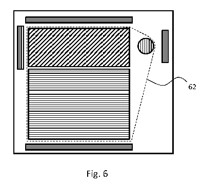
Finally, Fig. 6 illustrates a primary propagation zone 62, which is laterally
spanned by the
in-coupling, out-coupling and EPE gratings (i.e. a zone fully enclosing the
gratings with
minimum circumference; like a rubber band placed around the gratings). Thus,
the
primary route is entirely defined by these gratings together with properties
of the
CA 03087595 2020-07-03
WO 2019/155117 PCT/F12019/050065
9
waveguide, whereby the primary propagation path of the rays remains inside
this zone.
The mirror gratings are located outside this zone. It is however not excluded
that some
portions of the mirror gratings would be inside the primary propagation zone
62, as the
case might be in the configuration of Fig. 2B, for example. However,
typically, at least
50%, such as at least 75% of each mirror grating is outside this zone 62.
In some applications, in which large exit pupil is not required, the EPE
grating can be
omitted.
Instead or in addition to an EPE grating, the element may comprise one or more
intermediate gratings adapted to modify the light field inside the waveguide.
One or more
.. additional grating mirrors may be associated with such additional gratings.
While in typical embodiments, which are beneficial in terms of simplicity of
manufacturing,
the grating mirror is located on the same surface of the waveguide than the
grating it is
associated with, it can also be located on the other surface. It is also not
excluded that
there are mirror gratings on both surfaces.
It should be noted that the invention is applicable also in various other
display geometries
and configurations. For example, the field-of-view (FOV) or total wavelength
range can be
split by a suitable grating arrangement such that the FOV or wavelengths
propagate at
least partly along different routes. In these cases, the mirror gratings and
principles herein
discussed can be used for all these gratings and routes separately.
In the case of multilayer waveguides, each layer carrying for example a
different
wavelength band, embodiments of the invention can be applied separately to
each layer.
Embodiments of the invention are usable both with broadband illumination and
narrowband (including narrow multi-band) illumination and projectors.
The waveguide can be a planar piece of transparent material, typically plastic
or glass,
.. having two parallel main surfaces. All gratings 52, 53A-D, 54, 56 can be
fabricated for
example as surface relief gratings (SRGs) or by providing additional material
onto the
surface as diffractive features, or other diffractive optical elements (DOEs).
In one
example, the gratings comprise linear features made of at least one oxide or
nitride
material, such as TiO2, Si3N4, and Hf02, on a glass waveguide.