Language selection

Search

Patent 3087609 Summary

Third-party information liability

Some of the information on this Web page has been provided by external sources. The Government of Canada is not responsible for the accuracy, reliability or currency of the information supplied by external sources. Users wishing to rely upon this information should consult directly with the source of the information. Content provided by external sources is not subject to official languages, privacy and accessibility requirements.

Claims and Abstract availability

Any discrepancies in the text and image of the Claims and Abstract are due to differing posting times. Text of the Claims and Abstract are posted:

  • At the time the application is open to public inspection;
  • At the time of issue of the patent (grant).
(12) Patent Application: (11) CA 3087609
(54) English Title: WAVEGUIDE ELEMENT AND WAVEGUIDE STACK FOR DISPLAY APPLICATIONS
(54) French Title: ELEMENT DE GUIDE D'ONDES ET EMPILEMENT DE GUIDES D'ONDES POUR APPLICATIONS D'AFFICHAGE
Status: Application Compliant
Bibliographic Data
(51) International Patent Classification (IPC):
  • G02B 27/00 (2006.01)
  • G02B 5/18 (2006.01)
  • G02B 6/00 (2006.01)
  • G02B 27/01 (2006.01)
  • G02B 27/10 (2006.01)
  • G02B 27/42 (2006.01)
(72) Inventors :
  • BLOMSTEDT, KASIMIR (Finland)
  • OLKKONEN, JUUSO (Finland)
(73) Owners :
  • DISPELIX OY
(71) Applicants :
  • DISPELIX OY (Finland)
(74) Agent: ROBIC AGENCE PI S.E.C./ROBIC IP AGENCY LP
(74) Associate agent:
(45) Issued:
(86) PCT Filing Date: 2019-03-08
(87) Open to Public Inspection: 2019-10-03
Availability of licence: N/A
Dedicated to the Public: N/A
(25) Language of filing: English

Patent Cooperation Treaty (PCT): Yes
(86) PCT Filing Number: PCT/FI2019/050188
(87) International Publication Number: WO 2019185977
(85) National Entry: 2020-07-03

(30) Application Priority Data:
Application No. Country/Territory Date
20185295 (Finland) 2018-03-28

Abstracts

English Abstract

The invention relates to a waveguide display element comprising a waveguide body and an in-coupling grating (21) arranged to the waveguide body. The in-coupling grating (21) is configured to couple incoming light into the waveguide body into two separate directions (26A, 26B) using opposite diffraction orders (IC:+1, IC:-1) for splitting the field of view of the incoming light. Further the in-coupling grating (21) is configured, typically by setting its period suitably short, such that said coupling takes place only at wavelengths below a threshold wavelength residing in the visible wavelength range. The invention also relates to a waveguide stack (51 A, 51 B, 51 C).


French Abstract

L'invention concerne un élément d'affichage à guide d'ondes comprenant un corps de guide d'ondes et un réseau d'injection par couplage (21) disposé sur le corps de guide d'ondes. Le réseau d'injection par couplage (21) est configuré pour coupler la lumière entrante dans le corps de guide d'ondes dans deux directions séparées (26A, 26B) en utilisant des ordres de diffraction opposés (IC:+1, IC:-1) afin de diviser le champ de vision de la lumière entrante. En outre, le réseau d'injection par couplage (21) est configuré, habituellement en réglant sa période suffisamment courte, de telle sorte que ledit couplage a lieu uniquement à des longueurs d'onde inférieures à une longueur d'onde de seuil résidant dans la plage de longueurs d'onde visibles. L'invention concerne également un empilement de guides d'ondes (51 A, 51 B, 51 C).

Claims

Note: Claims are shown in the official language in which they were submitted.

CA 03087609 2020-07-03
WO 2019/185977 PCT/F12019/050188
6
Claims
1. A waveguide display element comprising
¨ a waveguide body,
¨ an in-coupling grating arranged to the waveguide body,
wherein the in-coupling grating is configured to couple incoming light into
the waveguide
body into two separate directions using opposite diffraction orders for
splitting the field of
view of the incoming light, the grating further being configured such that
said coupling
takes place only at wavelengths below a threshold wavelength residing in the
visible
wavelength range, wherein the in-coupling grating has a period, which is short
enough to
prevent coupling of wavelengths above said threshold wavelength into the
waveguide
body.
2. The element according to claim 1, wherein the threshold wavelength is in
the range of
500-540 nm or 620-660 nm, such as 510-530 nm or 630-650 nm, for example 520 nm
or
640 nm.
3. The element according to any of the preceding claims, wherein the waveguide
body
has an index of refraction higher than 1.8, such as 1.9 - 2.1.
4. The element according to any of the preceding claims, further comprising
¨ two first reflective gratings or first exit pupil expander gratings on
different sides of
the in-coupling grating corresponding to said separate directions,
¨ at least one second exit pupil expander grating adapted to receive light
from the
two first reflective gratings or exit pupil expander gratings, respectively,
¨ a single out-coupling grating adapted to receive light from the at least
one second
exit pupil expander grating.
5. The element according to claim 4, comprising a single second exit pupil
expander
grating.
6. The element according to claim 5, comprising two second exit pupil expander
gratings
at least partly on different sides of the out-coupling grating.
7. The element according to claim 6, wherein the second exit pupil expander
gratings
extend to the opposite side of the out-coupling grating, as seen from the
first exit pupil
expander gratings.

CA 03087609 2020-07-03
WO 2019/185977 PCT/F12019/050188
7
8. The element according to claim 6 or 7, wherein at least part of the light
is adapted to
travel from the first exit pupil expander gratings to the second exit pupil
expander gratings
via a region of the waveguide layer on which the out-coupling grating is
located, and
further back to the out-coupling grating.
9. The element according to any of the preceding claims, wherein the in-
coupling gratings
are adapted to couple light into the waveguide layers using the first positive
and first
negative diffraction orders, such as the first positive and negative
transmission diffraction
orders.
10. A waveguide stack for diffractive displays, the stack comprising at least
two
waveguide layers, wherein at least one of the waveguide layers is a waveguide
element
according to any of the preceding claims.
11. The stack according to claim 10, comprising at least three waveguide
layers at least
two of which are according to any of claims 1 - 9 and have different threshold
wavelengths.
12. The stack according to claim 11, wherein
¨ a first of the waveguide layers comprises a first in-coupling grating
adapted to
couple light to a first waveguide layer only below a first threshold
wavelength,
¨ a second of the waveguide layers comprises a second in-coupling grating
adapted
to couple light to a second waveguide layer only below a second threshold
wavelength higher than the first threshold wavelength,
¨ a third waveguide layer comprises an in-coupling grating configured to
couple light
to a third waveguide layer above said second threshold wavelength,
the stack further comprising
¨ a first wavelength filter element arranged between the first and the
second
waveguide layer and arranged to prevent wavelengths below the first threshold
wavelength entering the second in-coupling grating,
¨ a second wavelength filter element arranged between the second and the
third
waveguide layer and arranged to prevent wavelengths below the second threshold
wavelength entering the third in-coupling grating.
13. The stack according to claim 12, wherein the first and/or second
wavelength filter is a
reflective filter or absorptive filter.

CA 03087609 2020-07-03
WO 2019/185977 PCT/F12019/050188
8
14. A see-through display device comprising
¨ a waveguide element or waveguide stack according to any of the preceding
claims,
¨ a waveguide display image projector directed at the in-coupling grating
and being
capable of presenting a multicolor image comprising wavelengths both above and
below said threshold wavelength.

Description

Note: Descriptions are shown in the official language in which they were submitted.


CA 03087609 2020-07-03
WO 2019/185977 PCT/F12019/050188
1
Waveguide element and waveguide stack for display applications
Field of the Invention
The invention relates to waveguide-based displays. In particular, the
invention relates to a
light in-coupling arrangement for use in such displays. The invention can be
used in
modern personal displays, such as head-mounted displays (HMDs) and head-up
displays
(HUDs).
Background of the Invention
To maximize the field of view of see-through augmented reality (AR) displays
based on
diffractive waveguides, a common approach is to use multiple waveguides
stacked on top
of each other. To make the optimization process manageable, it is desirable
that each
lightguide in-couples only a single wavelength (e.g. laser light) or a narrow
wavelength
band (e.g. spectrum of a single color led). Some approaches based on
polarization has
been presented earlier, e.g. in US 2014/0064655 Al. Typically, surface relief
gratings are
not very polarization sensitive over a large field of view (FOV) which causes
cross-
coupling between the plates and leads to color variations over a uniform white
image.
Some conventional in-coupling solutions also require a relatively large area
on the
waveguide and/or set some undesired restrictions on the form factor of the
waveguide,
limiting their use in practical applications.
Thus, there is a need for improved in-coupling schemes.
Summary of the Invention
It is an aim of the invention to address the abovementioned problem and in
particular to
provide a novel waveguide element and waveguide stack by which cross-coupling
can be
reduced and/or the waveguide surface area used better.
According to a one aspect, there is provided a waveguide display element
comprising a
waveguide body and an in-coupling grating arranged to the waveguide body. The
in-
coupling grating is configured to couple incoming light into the waveguide
body into two
separate directions using opposite diffraction orders for splitting the field
of view of the

CA 03087609 2020-07-03
WO 2019/185977 PCT/F12019/050188
2
incoming light. Further the in-coupling grating is configured, typically by
setting its period
suitably short, such that said coupling takes place only at wavelengths below
a threshold
wavelength residing in the visible wavelength range.
According to another aspect, there is provided a waveguide stack for
diffractive displays,
the stack comprising at least two waveguide layers, wherein at least one of
the waveguide
layers is a waveguide element of the above kind.
According to a further aspect, there is provided a see-through display device
comprising a
waveguide or stack as discussed above, and a multicolor image projector
directed at the
in-coupling grating.
In particular, the invention is characterized by what is stated in the
independent claims.
The invention offers significant benefits. Most notably, it provides a
selective in-coupler
usable for realization of high-quality user-friendly multi-color displays. In
particular, cross-
coupling between layers is prevented while maintaining the ability to provide
a large FOV.
The dependent claims are directed to selected embodiments of the invention.
In some embodiments, the threshold wavelength is selected from the range of
500-540
nm or 620-660 nm, such as 510-530 nm or 630-650 nm. The threshold wavelength
can be
e.g. 520 nm or 640 nm. This provides the possibility to separate blue and
green, and, on
the other hand, green and red wavelengths from each other. In particular the
first
separation has been challenging in high-FOV applications due to the
overlapping
wavelength ranges of the colors, in particular when uncoherent LED light
sources are
used.
In some embodiments, the waveguide body is made of transparent material having
an
index of refraction higher than 1.8, such as 1.9 - 2.1.
In some embodiments, the element further comprises two first reflective
gratings or first
exit pupil expander gratings on different sides of the in-coupling grating
corresponding to
said separate directions, at least one second exit pupil expander gratings
adapted to
receive light from the two first gratings, respectively, and a single out-
coupling grating
adapted to receive light from the at least one second exit pupil expander
grating. The out-
coupling grating reconstructs the field of view split in the in-coupler.
Typically, there is
either a single second exit pupil expander grating or two second exit pupil
expander
gratings at least partly on different sides of the out-coupling gratings, in
which case the

CA 03087609 2020-07-03
WO 2019/185977 PCT/F12019/050188
3
second exit pupil expander gratings may extend to the opposite side of the out-
coupling
grating, as seen from the first gratings. This helps to optimize the usage of
the surface
area of the waveguide for practical applications, since at least part of the
light is adapted
to travel from the first exit pupil expander gratings to the second exit pupil
expander
gratings via a region of the waveguide layer on which the out-coupling grating
is located,
and further back to the out-coupling grating.
In some embodiments, the in-coupling gratings are adapted to couple light into
the
waveguide layers using the first positive and first negative diffraction
orders, such as the
first positive and negative transmission diffraction orders.
Next, embodiments of the invention and advantages thereof are discussed in
more detail
with reference to the attached drawings.
Brief Description of the Drawings
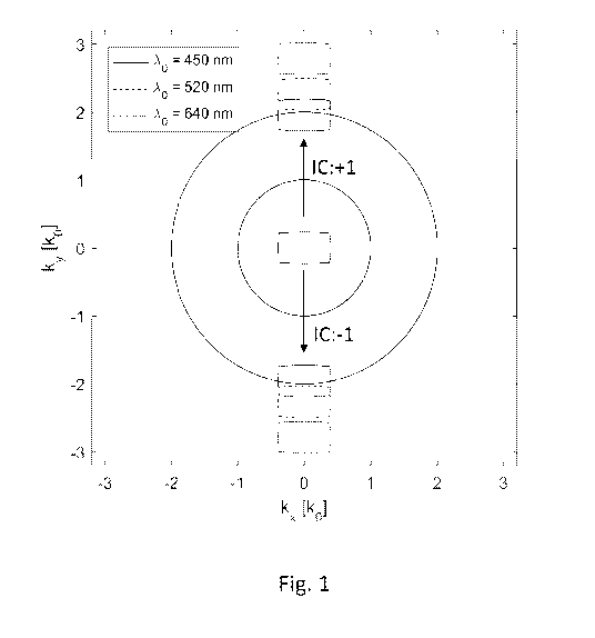
Fig. 1 shows a wave vector diagram illustrating the operation and benefit of
the present
invention according to one embodiment.
Fig. 2 illustrates in top view one practical waveguide layout having a single
second EPE
grating.
Fig. 3 illustrates in top view of another practical waveguide layout having a
two second
EPE gratings.
Fig. 4 shows a wave vector diagram illustrating the operation and benefit of
the
embodiment of Fig. 3.
Fig. 5 illustrates in a side view a waveguide stack according to one
embodiment.
Detailed Description of Embodiments
In one embodiment, the present approach comprises uniquely in-coupling only
wavelengths below a threshold value using an in-coupler that splits FOV into
two parts by
+/-1st diffraction orders and exhibits such a small grating period that
wavelengths above
the threshold value experience only the zeroth order diffraction.
This is illustrated in Fig. 1 that shows the wave vector analysis for the in-
coupling grating
that has a grating vector parallel to the y-axis. It is assumed that the
lightguide has

CA 03087609 2020-07-03
WO 2019/185977 PCT/F12019/050188
4
refractive index of 2.0, it resides in the xy-plane, and the virtual image has
52 deg
diagonal FOV with 16:9 aspect ratio. The +/-1st orders moves the FOV box from
the
center into the annulus. The inner radius of annulus is defined by the
refractive index of air
(=1.0) and the outer radius by the refractive index of the waveguide (=2.0).
The FOV
.. points inside the annulus propagate via total internal reflection inside
the waveguide. The
FOV points outside the annulus are forbidden modes that never exist. It can be
seen from
Fig. 1 that only wavelength below 520 nm couple into the lightguide. The total
FOV at 450
nm can be obtained by combining the FOV parts in-coupled by +/-1st orders. The
same
applies for all wavelengths that are smaller than 450 nm and still remain
inside the
annulus. This means that if the incident light, for instance, consists of
wavelength bands
B=[430,450] nm and G=[520,550] nm, then the in-coupler couples only B
wavelengths and
G wavelengths propagate through the grating with the zero order diffraction.
The presented in-coupling scheme can be used with traditional waveguide
grating
configurations. An example is given in Fig. 2. The in-coupling grating 21 is
surrounded by
two reflective gratings 22, 23 that turn the in-coupled light rays 26A, 26B on
the exit pupil
expansion (EPE) grating 24 that finally turns the light rays 27B, 28B on the
out-coupling
grating 25.
An alternative scheme is presented in Fig. 3. The in-coupling grating 31 is
accompanied
with first EPE gratings 32A, 32B that turn and expand light on the second EPE
gratings
33A, 33B. Light is out-coupled by the out-coupling grating 34A. By properly
selecting the
gratings vectors in this configuration, light rays can be fed through the out-
coupler on the
EPE gratings 33A, 33B without any diffraction. This can be seen from the wave
vector
analysis example shown in Fig. 4. Out-coupler diffracts the light rays coming
from the first
EPE gratings out-side the annulus, i.e. no diffraction occurs. Light
transportation through
the out-coupler on the EPE gratings enables smaller grating areas and thus
better form
factor for the waveguide.
The illustrated in-coupling scheme can be directly utilized in a RGB wave
guide stack.
Fig. 5 shows an exemplary stack. Waveguides 51A, 51B, and 510 are designated
for
blue, green and red light respectively and they contain in-coupling gratings
52A, 52B,
.. 520. To prevent blue light to in-couple waveguides of green and red light,
an optical filter
53A that reflects the blue light back to the waveguide 51A is placed between
the
waveguides 51A and 51B. In a similar manner, the optical filter that reflects
green light is
placed between the waveguides 51B and 510. The waveguide 510 receives only red
light. The filters 53A and B can be also absorptive filters.

CA 03087609 2020-07-03
WO 2019/185977 PCT/F12019/050188
All the presented embodiments can be utilized with both uncoherent (LED) and
coherent
(laser) light image projectors and projection schemes which are known in the
art of
waveguide displays.
Embodiments of the invention are most suitably used in see-through near-to-the-
eye
5 display (NED) devices or other HMDs.
Citations list
Patent literature
US 2014/0064655 Al

Representative Drawing
A single figure which represents the drawing illustrating the invention.
Administrative Status

2024-08-01:As part of the Next Generation Patents (NGP) transition, the Canadian Patents Database (CPD) now contains a more detailed Event History, which replicates the Event Log of our new back-office solution.

Please note that "Inactive:" events refers to events no longer in use in our new back-office solution.

For a clearer understanding of the status of the application/patent presented on this page, the site Disclaimer , as well as the definitions for Patent , Event History , Maintenance Fee  and Payment History  should be consulted.

Event History

Description Date
Compliance Requirements Determined Met 2024-04-20
Letter Sent 2024-03-08
Common Representative Appointed 2020-11-07
Inactive: Cover page published 2020-09-08
Letter sent 2020-07-24
Inactive: IPC assigned 2020-07-23
Request for Priority Received 2020-07-23
Priority Claim Requirements Determined Compliant 2020-07-23
Inactive: IPC assigned 2020-07-23
Application Received - PCT 2020-07-23
Inactive: First IPC assigned 2020-07-23
Inactive: IPC assigned 2020-07-23
National Entry Requirements Determined Compliant 2020-07-03
Application Published (Open to Public Inspection) 2019-10-03

Abandonment History

There is no abandonment history.

Maintenance Fee

The last payment was received on 

Note : If the full payment has not been received on or before the date indicated, a further fee may be required which may be one of the following

  • the reinstatement fee;
  • the late payment fee; or
  • additional fee to reverse deemed expiry.

Please refer to the CIPO Patent Fees web page to see all current fee amounts.

Fee History

Fee Type Anniversary Year Due Date Paid Date
Basic national fee - standard 2020-07-03 2020-07-03
MF (application, 2nd anniv.) - standard 02 2021-03-08 2020-07-03
MF (application, 3rd anniv.) - standard 03 2022-03-08 2022-03-04
MF (application, 4th anniv.) - standard 04 2023-03-08 2023-03-03
MF (application, 5th anniv.) - standard 05 2024-03-08
Owners on Record

Note: Records showing the ownership history in alphabetical order.

Current Owners on Record
DISPELIX OY
Past Owners on Record
JUUSO OLKKONEN
KASIMIR BLOMSTEDT
Past Owners that do not appear in the "Owners on Record" listing will appear in other documentation within the application.
Documents

To view selected files, please enter reCAPTCHA code :


To view images, click a link in the Document Description column. To download the documents, select one or more checkboxes in the first column and then click the "Download Selected in PDF format (Zip Archive)" or the "Download Selected as Single PDF" button.

List of published and non-published patent-specific documents on the CPD .

If you have any difficulty accessing content, you can call the Client Service Centre at 1-866-997-1936 or send them an e-mail at CIPO Client Service Centre.


Document
Description 
Date
(yyyy-mm-dd) 
Number of pages   Size of Image (KB) 
Drawings 2020-07-03 5 92
Claims 2020-07-03 3 95
Description 2020-07-03 5 202
Abstract 2020-07-03 2 65
Representative drawing 2020-07-03 1 13
Cover Page 2020-09-08 2 44
Commissioner's Notice: Request for Examination Not Made 2024-04-19 1 518
Commissioner's Notice - Maintenance Fee for a Patent Application Not Paid 2024-04-19 1 567
Courtesy - Letter Acknowledging PCT National Phase Entry 2020-07-24 1 588
Patent cooperation treaty (PCT) 2020-07-03 4 143
National entry request 2020-07-03 6 178
Patent cooperation treaty (PCT) 2020-07-03 2 70
International search report 2020-07-03 5 146