Note: Descriptions are shown in the official language in which they were submitted.
I
THERMAL RADIATION DETECTORS WITH CARBON-NANOTUBE-BASED OPTICAL
ABSORBERS
TECHNICAL FIELD
[0001] The technical field generally relates to thermal radiation detectors
and, more particularly, to
thermal radiation detectors that include optical absorbers based on carbon
nanotubes (CNTs).
BACKGROUND
[0002] Thermal radiation detectors are devices that sense changes in an
electrical parameter in
response to temperature variations related to an amount of absorbed
electromagnetic radiation.
Common types of thermal radiation detectors include microbolometer detectors,
thermocouple/thermopile detectors, and pyroelectric detectors. These detectors
can allow for
uncooled and spectrally broadband operation in various commercial, industrial,
and military
applications. Arrays of thermal radiation detectors can be fabricated on a
substrate using common
integrated-circuit-based microfabrication techniques, such as photolithography
and surface
micromachining. Detector components may be successively deposited and
patterned using thin-film
.. deposition techniques paired with selective photoresist and sacrificial
etching processes. The
substrate may be pre-manufactured using complementary metal-oxide-
semiconductor (CMOS)
processes and provided with a readout integrated circuit (ROIC).
[0003] Thermal radiation detectors usually include optical absorbers to
enhance their sensitivity and
overall performance. Various types of materials and structures have been used
or studied for use as
optical absorbers, among which are porous metal blacks, such as gold black.
Porous metal-black
films can provide high-efficiency, low-thermal-mass broadband absorbers that
can be deposited at
low temperatures using chemical vapor deposition processes for use in various
applications in the
infrared and terahertz spectral ranges. However, their widespread use has been
hampered by
several limitations, including their fragility, thermal instability, and
sensitivity to high-intensity
.. radiation. These limitations can degrade their absorbing properties and
make them incompatible or
less compatible with wafer-level CMOS microfabrication processes and high-
temperature processing
and packaging. Carbon-based materials, such as carbon nanotubes (CNTs), have
been considered
as potential alternatives to metal-black films, owing to their desirable
mechanical, thermal, chemical,
electrical, and optical properties. However, despite their potential
advantages, challenges remain in
their use as optical absorbers in microfabricated thermal radiation detectors,
for example, related to
the control of the porosity, density, uniformity, and selective patterning of
CNT films on suspended
microstructures.
Date Recue/Date Received 2020-07-23
2
SUMMARY
[0001] The present description generally relates to thermal radiation
detectors, such as
microbolometer, thermocouple/thermopile, and pyroelectric detectors, with
passivated carbon-
nanotube-based optical absorbers.
[0002] In accordance with an aspect, there is provided a thermal radiation
detector including:
a substrate;
a platform suspended above the substrate;
a support structure holding the platform;
a temperature sensor disposed on the platform and having an electrical
parameter that varies in
accordance with a temperature of the temperature sensor;
an optical absorber in thermal contact with the temperature sensor and
configured to absorb
incoming electromagnetic radiation to generate heat to change the temperature
of the
temperature sensor, the optical absorber including carbon nanotubes; and
a passivation layer structure disposed over the optical absorber, wherein the
passivation layer
structure is made of a passivation material comprising a metal compound.
[0003] In accordance with another aspect, there is provided a thermal
radiation detector array
including a plurality of thermal radiation detectors such as described herein.
[0004] In accordance with another aspect, there is provided a microbolometer
detector including:
a substrate;
a platform suspended above the substrate;
a support structure holding the platform;
a thermistor disposed on the platform and having an electrical resistance that
varies with a
temperature of the thermistor;
an optical absorber in thermal contact with the thermistor and configured to
absorb incoming
electromagnetic radiation to generate heat to change the temperature of the
thermistor; and
a passivation layer structure disposed over the optical absorber and including
titanium oxide.
[0005] In accordance with another aspect, there is provided a method of
fabricating a thermal
radiation detector, including:
forming a sacrificial layer on a substrate;
forming a platform and a support structure on the sacrificial layer;
forming a temperature sensor on the platform, the temperature sensor having an
electrical
parameter that varies in accordance with a temperature of the temperature
sensor;
Date Recue/Date Received 2022-09-13
3
forming an optical absorber in thermal contact with the temperature sensor and
configured for
absorbing incoming electromagnetic radiation to generate heat to change the
temperature of
the temperature sensor, the optical absorber comprising carbon nanotubes;
forming a passivation layer structure over the optical absorber, wherein the
passivation layer
structure is made of a passivation material comprising a metal compound; and
removing the sacrificial layer to suspend the platform above the substrate by
the support structure
and release the thermal radiation detector.
[0006] Other method and process steps may be performed prior to, during or
after the method and
process steps described herein. The order of one or more of the steps may also
differ, and some of
the steps may be omitted, repeated, and/or combined, depending on the
application or the
characteristics of the device to be fabricated.
[0007] Other features and advantages of the present description will become
more apparent upon
reading of the following non-restrictive description of specific embodiments
thereof, given by way of
example only with reference to the appended drawings. Although specific
features described in the
above summary and the foregoing detailed description may be described with
respect to specific
embodiments or aspects, it should be noted that these specific features can be
combined with one
another, unless stated otherwise.
BRIEF DESCRIPTION OF THE DRAWINGS
[0008] Fig. 1 is a schematic cross-sectional elevation view of a thermal
radiation detector in
accordance with an embodiment, where the thermal radiation detector is a
microbolometer detector.
[0009] Figs. 2A to 2D illustrate steps of a process for fabricating the
thermal radiation detector of
Fig. 1.
[0010] Fig. 3 is a schematic cross-sectional elevation view of a thermal
radiation detector in
accordance with another embodiment, where the thermal radiation detector is a
microbolometer
detector having a double-platform structure.
[0011] Fig. 4 is a schematic cross-sectional elevation view of a thermal
radiation detector in
accordance with another embodiment, where the thermal radiation detector is a
microbolometer
detector having a stack of alternating optical absorber layers and passivation
layers.
[0012] Fig. 5 is a schematic cross-sectional elevation view of a thermal
radiation detector in
accordance with another embodiment, where the thermal radiation detector is a
microbolometer
detector having both a double-platform structure and a stack of alternating
optical absorber layers
and passivation layers.
Date Recue/Date Received 2022-09-13
4
[0016] Fig. 6A is a schematic cross-sectional elevation view of a thermal
radiation detector in
accordance with another embodiment, where the thermal radiation detector is a
thermopile detector.
Fig. 6B is a schematic top view of the thermal radiation detector of Fig. 6A,
in which components
have been omitted to illustrate the configuration of the thermopiles.
[0017] Fig. 7 is a schematic cross-sectional elevation view of a thermal
radiation detector in
accordance with another embodiment, where the thermal radiation detector is a
pyroelectric detector.
[0018] Fig. 8 is a schematic cross-sectional elevation view of an array of
thermal radiation detectors,
in accordance with an embodiment, where the thermal radiation detectors are
microbolometer
detectors.
[0019] Fig. 9 is a schematic cross-sectional elevation view of an array of
thermal radiation detectors,
in accordance with an embodiment, where the thermal radiation detectors are
thermopile detectors.
[0020] Fig. 10 is a schematic cross-sectional elevation view of an array of
thermal radiation
detectors, in accordance with an embodiment, where the thermal radiation
detectors are pyroelectric
detectors.
[0021] Fig. 11 is a scanning electron microscope image of a film of randomly
aligned CNTs prepared
by ultrasonic spray coating with n-methyl-pyrrolidone as a solvent, in
accordance with another
embodiment.
[0022] Fig. 12 shows a Fourier transform infrared (FTIR) reflectance spectrum
of a CNT film with a
random arrangement of CNTs and having a thickness of about 2 micrometers (pm)
in accordance
with another embodiment, where the CNT film was formed by spray coating.
[0023] Fig. 13 shows an FTIR reflectance spectrum of a CNT film with a random
arrangement of
CNTs and having a thickness of about 300 pm, in accordance with another
embodiment, where the
CNT film was formed by a film transfer technique.
[0024] Fig. 14 shows four FTIR reflectance spectra of a CNT film having a
random arrangement of
CNTs and a thickness of about 2 pm. The CNT film was formed by spray coating.
One of the spectra
was obtained without subjecting the CNT film to a heat treatment. The other
three spectra were
obtained after having successively cured the CNT film for an hour at 150 C,
250 C, and 350 C,
respectively.
[0025] Fig. 15 shows four FTIR reflectance spectra of a CNT film. One of the
spectra was obtained
after sputter deposition of a titanium layer on the CNT film. The other
spectra were obtained after
Date Recue/Date Received 2020-07-23
5
successively subjecting the titanium-coated CNT film to oxygen plasma in a
plasma asher system for
15 minutes, 40 hours, and 80 hours, respectively.
[0026] Fig. 16 is an optical microscope image of an array of passivated CNT-
based optical absorbers
formed on a six-inch silicon wafer substrate and patterned by a
photolithography and etching process.
DETAILED DESCRIPTION
[0027] In the present description, similar features in the drawings have been
given similar reference
numerals. To avoid cluttering certain figures, some elements may not be
indicated if they were
already identified in a preceding figure. It should also be understood that
the elements of the drawings
are not necessarily depicted to scale, since emphasis is placed on clearly
illustrating the elements
and structures of the present embodiments. Furthermore, positional descriptors
indicating the
location and/or orientation of one element with respect to another element are
used herein for ease
and clarity of description. Unless otherwise indicated, these positional
descriptors should be taken in
the context of the figures and should not be considered limiting. As can be
appreciated, such spatially
relative terms are intended to encompass different orientations in the use or
operation of the present
embodiments, in addition to the orientations exemplified in the figures.
Furthermore, when a first
element is referred to as being "on", "above", "below", "over", or "under" a
second element, the first
element can be either directly or indirectly on, above, below, over, or under
the second element,
respectively, such that one or multiple intervening elements may be disposed
between the first
element and the second element.
[0028] The terms "a", "an", and "one" are defined herein to mean "at least
one", that is, these terms
do not exclude a plural number of elements, unless stated otherwise.
[0029] Terms such as "substantially", "generally", and "about", that modify a
value, condition, or
characteristic of a feature of an exemplary embodiment, should be understood
to mean that the value,
condition, or characteristic is defined within tolerances that are acceptable
for the proper operation
of this exemplary embodiment for its intended application or that fall within
an acceptable range of
experimental error. In particular, the term "about" generally refers to a
range of numbers that one
skilled in the all would consider equivalent to the stated value (e.g., having
the same or equivalent
function or result). In some instances, the term "about" means a variation of
10% of the stated value.
It is noted that all numerical values used herein are assumed to be modified
by the term "about",
unless stated otherwise.
[0030] The terms "connected" and "coupled", and derivatives and variants
thereof, are intended to
refer herein to any connection or coupling, either direct or indirect, between
two or more elements,
Date Recue/Date Received 2020-07-23
6
unless stated otherwise. For example, the connection or coupling between the
elements may be
mechanical, optical, electrical, magnetic, thermal, chemical, logical,
fluidic, operational, or any
combination thereof.
[0031] The terms "light" and "optical", and variants and derivatives thereof,
are intended to refer
herein to radiation in any appropriate region of the electromagnetic spectrum.
These terms are not
limited to visible light, but may also include, without being limited to, the
infrared, terahertz and
millimeter wave regions. By way of example, in some embodiments, the present
techniques may be
used with electromagnetic radiation having a center wavelength ranging from
about 0.2 pm to about
3000 pm. Infrared radiation is commonly divided into various regions,
including the near-infrared
(NI R) region for wavelengths ranging from 0.7 to 1.4 pm; the short-wavelength
infrared (SWIR) region
for wavelengths ranging from 1.4 to 3 pm; the mid-wavelength infrared (MWIR)
region for
wavelengths ranging from 3 to 8 pm; the long-wavelength infrared (LWIR) region
for wavelengths
ranging from 8 to 15 pm; and the far-infrared (FIR) region for wavelengths
ranging from 15 to
1000 pm. It is appreciated that the definitions of different infrared regions
in terms of spectral ranges,
as well as their limits, may vary depending on the technical field under
consideration, and are not
meant to limit the scope of application of the present techniques. It is also
appreciated that although
several embodiments of the present techniques may be useful in infrared
applications, other
embodiments could additionally or alternatively operate in other regions of
the electromagnetic
spectrum, for example, in the terahertz region.
[0032] The present description generally relates to thermal radiation
detectors with passivated
carbon-nanotube-based optical absorbers. As described in greater detail below,
a thermal radiation
detector in accordance with an embodiment may include a substrate, a platform
suspended above
the substrate by a support structure, a temperature sensor disposed on the
platform, an optical
absorber including CNTs and configured to absorb electromagnetic radiation to
heat up the
temperature sensor, and a passivation layer structure formed on the optical
absorber.
[0033] The provision of a passivation layer structure may protect or help
protect the integrity of the
optical absorber during the release of the suspended platform. The platform
release process typically
includes a step of etching a sacrificial layer on which the platform is
formed. Sacrificial layer etching
is often performed in an oxygen-rich environment, for example, in an oxygen
plasma, which could
otherwise damage or adversely affect the CNTs forming the optical absorber
without the provision of
a passivation layer structure. In one embodiment, the CNTs may be formed as a
film (e.g., by spray
coating) and the passivation layer structure may be formed on the CNT film by
deposition of a metal
layer (e.g., by sputtering) followed by an oxidation process (e.g., by oxygen
plasma treatment) to
convert the metal layer to a metal oxide layer. For example, the metal layer
may be made of titanium
Date Recue/Date Received 2020-07-23
7
(Ti) or aluminum (Al) and the metal oxide layer may be made of titanium oxide
(e.g., titanium dioxide,
TiO2) or aluminum oxide (e.g., alumina, A1203). Alternatively, the passivation
layer structure may be
formed on the CNT film by deposition of a metal oxide layer, for example, a
titanium oxide or
aluminum oxide layer, optionally followed by an oxidation process. Depending
on the desired or
required thickness for the optical absorber, a multilayer stack of alternating
layers of CNTs and
passivation layers may be formed through a series of deposition,
photolithography, and etching steps
to enhance or otherwise control the absorption spectrum and the passivation
properties of the stack.
[0034] The term "thermal radiation detector" generally refers herein to a
detector of electromagnetic
radiation that includes an optical absorber and a temperature sensor or
transducer. The optical
absorber is configured to absorb the radiation and convert the absorbed
radiation into heat. The
temperature sensor is in thermal contact with the optical absorber and has an
electrical parameter
that varies in accordance with its temperature. When heated by the optical
absorber, the temperature
of the temperature sensor increases. This produces a change in the electrical
parameter, which can
then be measured electrically. Several types of thermal radiation detectors
exist, which may be
categorized according to the nature and operating principles of the
temperature sensor. Non-limiting
examples of thermal radiation detectors include microbolometer detectors,
which include thermistors
operating based on the thermoresistive effect, thermocouple/thermopile
detectors, which include one
or more thermocouples operating based on the Seebeck effect, pyroelectric
detectors, which operate
based on the pyroelectric effect, and piezoelectric temperature detectors,
which operate based on
the piezoelectric effect. It is appreciated that the theory, structure,
operation, and applications of such
thermal radiation detectors are generally known in the art, and need not be
described in detail herein
other than to facilitate an understanding of the present techniques. It is
also appreciated that the use
of the term "thermal" refers to the fact that the operation of the thermal
radiation detectors disclosed
herein involves the conversion of electromagnetic radiation into heat. In
particular, the term "thermal"
does not mean that the thermal radiation detectors disclosed herein are
limited to detecting "thermal
radiation", which is a term whose scope is sometimes limited to infrared
radiation. Rather, the thermal
radiation detectors disclosed herein may be configured to detect
electromagnetic radiation in any
appropriate region of the spectrum.
[0035] The present techniques have potential use in various commercial,
industrial, and military
applications that may benefit from or require thermal radiation detectors with
enhanced optical
absorbers. Non-limiting examples of possible fields of use include, to name a
few, defense and
security, aerospace and astronomy, inspection and maintenance, night vision,
transportation,
pollution and fire detection, spectroscopy, remote sensing, industrial
control, robotics, medicine,
sports and entertainment, food supply chain management, and the Internet of
Things.
Date Recue/Date Received 2020-07-23
8
[0036] Various aspects, features, and implementations of the present
techniques are described
below with reference to the figures.
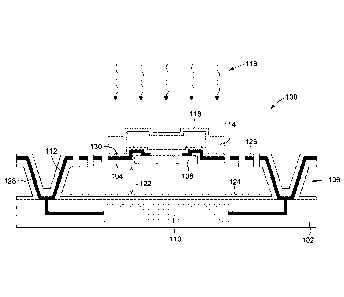
[0037] Referring to Fig. 1, there is illustrated a schematic view of a
possible embodiment of a thermal
radiation detector 100. In this embodiment, the thermal radiation detector 100
is implemented as a
microbolometer detector. The thermal radiation detector 100 of Fig. 1 may be
used as an individual
pixel (photosensitive element) of a microbolometer array of a thermal camera
or imaging device. In
the present description, the term "microbolometer" is intended to refer to a
thermal radiation detector
whose temperature sensor is a thermistor, which is a piece of material whose
electrical resistance
changes in response to temperature variations caused by the heat generated by
the absorbed
.. radiation. Microbolometers can be classified as either cooled or uncooled,
depending on whether
their operation involves cooling or not. It is also appreciated that, in the
present description, the terms
"microbolometer" and "bolometer" can generally be used interchangeably.
[0038] The thermal radiation detector 100 of Fig. 1 is formed as a stack of
layers deposited on a
substrate 102. The thermal radiation detector 100 generally includes a
substrate 102, a suspended
platform 104, a support structure 106 configured to hold the platform 104
above the substrate 102, a
temperature sensor or transducer 108 disposed on the platform 104, an
electrical readout circuit 110
located in the substrate, an electrode structure 112 electrically connecting
the temperature
sensor 108 to the electrical readout circuit 110, an optical absorber 114 in
thermal contact with the
temperature sensor, and a passivation layer structure 116 disposed over the
optical absorber 114.
The structure, composition, and operation of these and other possible
components of the thermal
radiation detector 100 are described in greater detail below.
[0039] Thermal radiation detectors such as the one depicted in Fig. 1 may be
fabricated using
common integrated-circuit and microfabrication techniques, such as surface and
bulk
micromachining. In such techniques, detector components can be successively
deposited and
.. patterned on a substrate using thin-film deposition techniques paired with
selective photoresist and
sacrificial layer etching processes. In some applications, thermal radiation
detectors can be
fabricated using a monolithic integration approach in which the substrate,
typically provided with an
underlying readout integrated circuit (ROIC), is pre-manufactured using
complementary metal-oxide-
semiconductor (CMOS) processes. It is appreciated that various other
fabrication techniques may be
.. used, including those based on silicon-on-insulator, GaAs, GaN, InP, and
SiC techniques.
[0040] Figs. 2A to 2D illustrate possible steps of a method of fabricating a
thermal radiation
detector 100, such as the one of Fig. 1. The method may include a step of
forming a sacrificial
layer 120 on a substrate 102, followed by subsequent steps of forming a
platform 104 and a support
Date Recue/Date Received 2020-07-23
9
structure 106, and the temperature sensor 108 may each include a series of
deposition,
photolithography pattern, and etching operations. The method may also include
a step of forming an
optical absorber 114 including carbon nanotubes and disposed in thermal
contact with the
temperature sensor 108 (see Fig. 2B). As noted above, the optical absorber 114
is configured for
absorbing incoming electromagnetic radiation to heat up the temperature sensor
108 and change its
electrical response. The method may further include a step of forming a
passivation layer
structure 116 over the optical absorber 114 (see Fig. 2C). The method may also
include a step of
removing the sacrificial layer 120 to suspend the platform 104 above the
substrate 102 by the support
structure 106 and release the thermal radiation detector 100 (Fig. 20).
[0041] Returning to Fig. 1, the substrate 102 provides mechanical support for
the other components
of the thermal radiation detector 100. The substrate 102 may be made of
silicon (Si), silicon carbide
(SIC), gallium arsenide (GaAs), gallium nitride (GaN), germanium (Ge), or
another suitable material
or combination of materials. For example, the substrate 102 may be a die
separated from a
semiconductor wafer, for example, a silicon wafer. In some implementations,
the substrate 102, as
.. well as other components of the thermal radiation detector 100 may be made
of a flexible material,
for example, a polymer material, such as disclosed in co-assigned U.S. Pat.
Appl.
Pub. No. 2020/0149973 Al. The electrical readout circuit 110 may be embodied
by one or more
CMOS circuitry layers formed in or on the substrate 102. The electrical
readout circuit 110 may
alternatively be provided outside of the substrate 102. The electrical readout
circuit 110 may be
.. configured to measure changes in an electrical parameter of the temperature
sensor 108 (e.g., its
electrical resistance when the temperature sensor 108 is a thermistor) in
response to temperature
variations thereof caused by heat generated from electromagnetic radiation 118
absorbed by the
optical absorber 114.
[0042] The platform 104 is suspended above the substrate 102 by the support
structure 106. The
term "platform" generally refers herein to a substantially planar, suspended
structure, typically having
greater horizontal dimensions than vertical thickness. In the present
description, the term "horizontal"
refers to directions lying in a plane generally parallel to the substrate 102,
while the term "vertical"
refers to a direction generally perpendicular to the plane of the substrate
102. The suspension of the
platform 104 above the substrate 102 provides thermal isolation to the
temperature sensor 108, in
order to enhance the detection sensitivity of the thermal radiation detector
100. The platform 104
may be a single or multilayer structure made of an electrically insulating,
mechanically self-supportive
Date Recue/Date Received 2022-09-13
10
and low-stress material, such as silicon nitride, silicon dioxide, silicon
oxynitride, a metal or metal
oxide. The platform 104 may have horizontal dimensions ranging from about 5 pm
to about
25 millimeters (mm), and a thickness ranging from about 0.05 pm to about 1 mm,
although other
dimensions may be used in other implementations. It is appreciated that the
platform 104 may be
provided in a variety of sizes, shapes, and configurations.
[0043] In the illustrated embodiment, the platform 104 is printed on top of a
sacrificial layer 120 (see
Fig. 2A). The sacrificial layer 120 may be formed on the substrate 102 during
the fabrication process
of the thermal radiation detector 100 and be subsequently etched, dissolved,
or otherwise removed
to define a gap 122 between the substrate 102 and the platform 104 (see Fig.
2D). The sacrificial
layer 120 may be made of polyimide or another suitable material, for example,
photoresist material
and other organic materials that can be etched in plasma etching process. The
sacrificial layer 120
may be removed using an oxygen plasma release process or another suitable
release process, for
example, a wet or dry etching process. Furthermore, a reflector 124 may be
deposited on the
substrate 102 under the platform 104. The reflector 124 may include a thin
metal film, for example, a
thin aluminum, gold, or silver film, which can form an optical resonant cavity
with the platform 104 to
enhance the optical absorption capabilities of the thermal radiation detector
100.
[0044] Referring still to Fig. 1, the platform 104 is held above the substrate
102 by the support
structure 106. In the present description, the term "support structure" is
used to refer broadly to a
structure configured to hold the platform 104 in a spaced-apart relationship
above the substrate 102.
For example, the support structure 106 may be configured to hold the platform
104 at a height
ranging from about 1 pm to about 5 mm above the substrate 102, although other
height values are
possible in other implementations. The support structure 106 also provides a
path for the electrode
structure 112 to connect the temperature sensor 108 to the electrical readout
circuit 110. Like the
platform 104, the support structure 106 may be made of a low-stress and self-
supporting material
such as silicon nitride or silicon dioxide. In some embodiments, it may be
convenient to describe the
support structure 106 as having arms 126 and posts 128. The terms "arm" and
"post" generally refer
herein to structural elements of the support structure 106 that extend mainly
horizontally and mainly
vertically, respectively. In Fig. 1, the support structure 106 includes arms
126 that extend outwardly
from opposite edges of the platform 104, and posts 128 connecting the arms 126
to the
substrate 102. It is appreciated, however, that the support structure 106 may
have a variety of
configurations to meet the mechanical, electrical, and/or thermal requirements
or preferences of a
given application. In particular, the arms 126 and posts 128 of the support
structure 106 may have
various sizes, shapes, and arrangements relative to the platform 104, and
their number can vary
depending on the application.
Date Recue/Date Received 2020-07-23
11
[0045] The temperature sensor 108 is disposed on the platform 104 and has an
electrical parameter
responsive to variations in its temperature resulting from the heat produced
by the absorption of the
electromagnetic radiation 118 by the optical absorber 114. The variations in
the electrical parameter
of the temperature sensor 108 can be measured by the electrical readout
circuit 110. In the
embodiment of Fig. 1, the temperature sensor 108 includes a thermistor
deposited on the
platform 104 and the temperature-sensitive electrical parameter is the
electrical resistance of the
thermistor. In the present description, the term "thermistor" is intended to
encompass any suitable
material, structure, or device having an electrical resistance that changes as
a function of its
temperature, generally in a predictable and controllable manner. The
thermistor may be made of a
material having a high temperature coefficient of resistance (TCR) at room
temperature, for example,
at least 0.5% per kelvin in absolute value. Non-limiting examples of
thermistor materials include, to
name a few, vanadium oxide, amorphous silicon, and titanium oxide. However,
other thermistor
materials or combinations of thermistor materials may be used in other
implementations including,
but not limited to, semiconductor-, ceramic-, polymer-, and metal-based
thermistors, with either
positive or negative TCRs. Although a single thermistor is illustrated in Fig.
1, a plurality of thermistors
may be provided in other embodiments. It is appreciated that the size, shape,
and arrangement of
the or each thermistor may be varied depending on the application.
[0046] The electrode structure 112 extends along the plafform 104, the arms
126, the posts 128, and
the substrate 102 to provide an electrically conductive path between the
temperature sensor 108 and
the electrical readout circuit 110. The electrode structure 112 may be formed
using common
microfabrication techniques and may be made from any suitable electrically
conducting material
including, to name a few, gold, aluminum, titanium, copper, silver, tungsten,
chrome, and vanadium.
It is appreciated that the size, shape, composition, and configuration of the
electrode structure 112
may be varied in accordance with the requirements or preferences of a given
application.
[0047] Referring still to Fig. 1, the optical absorber 114 is provided in
thermal contact with the
temperature sensor 108 and is configured to absorb the incoming
electromagnetic radiation 118 to
generate heat to increase the temperature of the temperature sensor 108. In
the present description,
the term "optical absorber" refers to a material or structure of the thermal
radiation detector which,
upon exposure to electromagnetic radiation within a certain waveband, absorbs
electromagnetic
energy from the electromagnetic radiation within that waveband and convert the
absorbed
electromagnetic energy into thermal energy. In the illustrated embodiment, the
optical absorber 114
is made of an absorber material that includes carbon nanotubes, as described
in greater detail below.
[0048] In the present description, the term "thermal contact" generally means
that heat conduction
occurs directly or indirectly between two elements, that is, the two elements
may be in direct contact
Date Recue/Date Received 2020-07-23
12
with each other or may have a sufficiently thermally conducting material
present between them.
Specifically, the term "thermal contact" is intended to refer to the fact that
when the optical
absorber 114 is heated upon absorption of electromagnetic radiation 118, the
heat thus generated is
conducted, radiated or otherwise transmitted to the temperature sensor 108. In
the embodiment of
Fig. 1, the optical absorber 114 is disposed on the platform 104 and over the
temperature
sensor 108. Depending on the application, the optical absorber 114 may be
either in direct contact
with the temperature sensor 108 or, as depicted in Fig. 1, separated from the
temperature sensor 108
by one or more intervening layers 130, for example, made of silicon nitride or
silicon dioxide.
[0049] Referring to Fig. 3, there is illustrated another embodiment of a
thermal radiation detector 100,
which is also implemented as a microbolometer detector. The embodiment of Fig.
3 shares several
features with the embodiment of Fig. 1, which will not be described again
other than to highlight
differences between them. The thermal radiation detector 100 generally
includes a substrate 102, a
platform 104, a support structure 106, a temperature sensor 108, an electrical
readout circuit 110, an
electrode structure 112, an optical absorber 114, and a passivation layer
structure 116, several of
which may be similar to those of Fig. 1. In Fig. 3, the thermal radiation
detector 100 further includes
an absorber platform 132 suspended above the platform 104 in a spaced
relationship therewith. The
optical absorber 114, which is composed of carbon nanotubes, is disposed on
the absorber
platform 132. The thermal radiation detector 100 of Fig. 3 also further
includes another support
structure 134 configured to hold the absorber platform 132. For example, the
absorber platform
support structure 134 may be configured to hold the absorber platform 132 at a
height ranging from
about 1 pm to about 25 pm above the platform 104, although other height values
are possible in other
implementations. The absorber platform 132 and its support structure 134 may
be made of a
mechanically self-supportive material, for example, silicon nitride, silicon
dioxide, or a metal.
[0050] The absorber platform 132 and the support structure 134 provide a
thermal conductance path
between the optical absorber 114 on the absorber platform 132 and the
temperature sensor 108 so
that the heat generated by the optical absorber 114 upon absorption of
electromagnetic radiation 118
can be transferred to the temperature sensor 108. The thermal conductance of
the absorber
platform 132 and its support structure 134 can be adjusted based on the
thermal requirements of a
given application. In the illustrated embodiment, the support structure 134
includes a post 136
projecting upwardly from a central region of the platform 104. The
configuration and disposition of
the support structure 134 can be varied in other embodiments, depending on the
requirements or
preferences of a given application. It is appreciated that compared to a
single-platform structure such
as the one depicted in Fig. 1, the provision of a double-platform structure
such as the one depicted
in Fig. 3 may improve the thermal insulation of the temperature sensor 108,
provide a higher fill factor
Date Recue/Date Received 2020-07-23
13
for optical absorption, and/or shield the support structure 106 during the
fabrication of the optical
absorber 114 and the passivation layer structure 116.
[0051] Returning to Fig. 1, the optical absorber 114 includes a CNT film. CNTs
have desirable
mechanical, thermal, chemical, electrical, and optical properties, which make
them interesting for a
broad range of applications. CNTs are known as efficient broadband optical
absorbers, notably in the
visible, infrared, and terahertz regions of the electromagnetic spectrum. The
absorption spectrum of
optical absorbers made of CNT-based films depend on a number of factors
including, for example,
the thickness of the CNT film and the diameter and length of the individual
CNTs.
[0052] In the present description, the term "carbon nanotube" (CNT) generally
refers to a hollow
article composed primarily of carbon atoms. CNTs are typically formed from
cylindrical layers of
graphene sheets. The individual sheets can vary in layering, morphology, and
functionality. CNTs
can exist as single-walled CNTs (SWCNTs) and multi-walled CNTs (MWCNTs). It is
appreciated that
the present techniques are not limited to specific types of CNTs. As such, the
optical absorber 114
can include any mixture of CNTs, where the individual CNTs in the mixture may
differ in diameter,
chirality, number of walls, and/or any other relevant parameters. CNTs can be
metallic, semi-metallic,
semi-conducting, or insulating. CNTs can also be chiral or achiral. CNTs can
be characterized by a
diameter and a length. The diameter may range from about 0.5 nm to about 100
nm and the length
may range from about 1 pm to about 50 pm. CNTs are composed primarily of
carbon atoms, but they
may be doped with other elements, for example, metals. CNTs may be synthesized
by a variety of
methods including, for example, chemical vapor deposition (CVD), arc
discharge, and laser ablation.
[0053] In Fig. 1, the optical absorber 114 includes a CNT film deposited on
the platform 104. In the
present description, the term "CNT film" may refer to any layered arrangement
of CNTs, including a
network, an array, a mesh, a grid, or a similar arrangement formed of
individual CNTs or bundles of
CNTs. Individual CNTs of a CNT film may or may not have identical or similar
properties. It is
appreciated that bundles of CNTs may tend to form spontaneously during
fabrication of CNT films.
In some implementations, the CNTs or CNT bundles may be randomly arranged
within the CNT film.
However, in other implementations, the CNTs or CNT bundles may be arranged or
aligned along one
or more predominant directions. In some implementations, the CNTs may be
horizontally stacked or
vertically stacked. Depending on the application, the distribution of CNTs or
CNT bundles in a CNT
film may be homogenous or inhomogeneous. The thickness of the CNT film forming
the optical
absorber 114 may range from about 0.2 pm to about 500 pm, although other
thickness values may
be used in other embodiments. CNT films can be prepared using various
techniques. These
techniques may be divided into two main categories: vapor phase deposition
methods and solution-
based coating methods. Vapor phase deposition methods include a variety of CVD
techniques using
Date Recue/Date Received 2020-07-23
14
mixtures of gas precursors in vacuum-based deposition systems. These growth
methods usually
involve high processing temperatures and can provide high-quality films with
vertically aligned
SWCNTs and/or MWCNTs with predefined properties. Solution-based coating
methods encompass
a variety of techniques including, but not limited to, spray coating, roll-to-
roll coating, dip coating, spin
coating, spray deposition, inkjet printing, transfer printing, screen
printing, sol-gel, vacuum filtration,
and electrophoretic deposition. Solution-based coating methods typically use
CNT-based
dispersions. Such dispersions are generally prepared using a mixture of
purified CNT powder,
obtained, for example, by CVD, and a wide variety of solvents and surfactants.
The solvents and
surfactants used can depend on various CNT parameters including, to name a
few, the chirality, the
functionalization radicals, the coating method, and the properties of the
surface or substrate to be
coated.
[0054] Referring still to Fig. 1, the thermal radiation detector 100 includes
a passivation layer
structure 116 disposed over the optical absorber 114. In the present
description, the term "layer" is
intended to refer broadly to any substantially planar or laminar structure
(e.g., the passivation layer
structure) which is disposed on an underlying structure (e.g., the optical
absorber) in a continuous or
non-continuous manner. The term "layer" is meant to include both a single
layer of particles and
multiple layers of particles and is intended to encompass, but is not limited
to, films and coatings.
Depending on the application, the thickness of the layer may vary or remain
substantially uniform
over the extent of the layer. The arrangement of the particles forming the
layer may be porous or
compact and may be homogenous or not. In some implementations, the layer
(e.g., the passivation
layer structure) can intermingle or mix to some degree with the underlying
structure (e.g., the optical
absorber) if the underlying structure is sufficiently porous. For example, in
some cases, the degree
of intermingling between the passivation layer structure and the optical
absorber may be sufficiently
high for them to be considered to form a composite structure.
[0055] The passivation layer structure 116 is configured for allowing the
electromagnetic
radiation 118 to pass therethrough to reach and be absorbed by the CNTs of the
optical
absorber 114. In the present description, the terms "transparent" and
"transparency", and variants
and derivatives thereof, refer to the capability of the passivation layer
structure of allowing
electromagnetic radiation in a certain spectral region to pass therethrough
and reach the optical
absorber without being appreciably reflected or absorbed. It is understood
that the term "transparent"
includes not only "completely transparent", but also "substantially
transparent" and "sufficiently
transparent". In particular, the term "transparent" in the context of an
exemplary embodiment should
be interpreted as indicating a degree of transparency that is sufficiently
high for the proper operation
of the optical absorber of this exemplary embodiment. It is appreciated that
the precise degree of
Date Recue/Date Received 2020-07-23
15
transparency of the passivation layer structure may depend on a variety of
factors, non-limiting
examples of which can include its composition, its thickness, its structure,
its fabrication process, and
the wavelength or waveband of the radiation that is being transmitted. For
example, in one
embodiment, the passivation layer structure may be substantially transparent
to electromagnetic
radiation having a wavelength ranging from about 0.2 pm to about 30 pm, and
particularly between
about 2 pm and about 14 pm.
[0056] The passivation layer structure 116 is also configured for providing a
protective barrier for the
CNTs, for example, during the process of releasing the platform 104. Platform
release may include
the etching or otherwise removal of a sacrificial layer on which the platform
104 was formed (see,
e.g., Figs. 2A to 2D). In common micromachining processes, organic sacrificial
layer removal may
be achieved by oxygen plasma etching or another removal process performed in
an oxygen-rich
environment or in another environment. It has been recognized by the inventors
that oxygen and
other oxygen species present in these processes may react with the carbon
atoms of the CNTs of
the optical absorber 114, for example, to form carbon dioxide, which may
degrade or otherwise
adversely affect the CNTs if the CNTs are not passivated or otherwise
protected. Furthermore, it is
noted that passivating CNTs can be challenging. One reason is that CNT films
are generally porous
and characterized by a non-uniform morphology, which can make the use of
conventional passivation
methods, such as those using CVD of silicon oxide and silicon nitride films,
difficult, impractical, or
impossible.
.. [0057] In one embodiment, the passivation layer structure 116 may be a thin-
film coating formed on
the optical absorber 114. The passivation layer structure 116 may have a
thickness sufficient to
impart passivation to the optical absorber 114 without or with only little
degradation in optical
absorption performance. For example, the thickness of the thin-film coating
can range from about
50 nm to about 200 nm. In general, the thickness of the passivation layer
structure 116 may be
adjusted to ensure or help ensure passivation efficiency, optical transparency
in the operating
waveband, and mechanical integrity. Depending on the application, the thin-
film coating forming the
passivation layer structure 116 can include a single-layer thin film or a
multilayer thin film.
[0058] It is appreciated that various types of passivating materials may be
used to form the
passivation layer structure 116. Non-limiting examples include metal
compounds, such as metal
oxides, metal nitrides, metal carbides, metal borides, and mixtures and
combinations thereof.
Depending on the application, the metal compounds may include stoichiometric
compounds, non-
stoichiometric compounds, or mixtures or stoichiometric and non-stoichiometric
compounds. More
specific examples of possible materials for the passivation layer structure
116 include titanium oxide,
Tix0y, (e.g., titanium dioxide, TiO2) and aluminum oxide, AlxOy, (e.g.,
alumina, A1203). It has been
Date Recue/Date Received 2020-07-23
16
found that the use of titanium oxide as a passivating material for CNT-based
optical absorbers can
be advantageous because titanium oxide has a high chemical resistance to
various etching gases
and solutions and is widely used in microfabrication processes. Thin films and
coatings of titanium
and titanium oxide may be deposited by various methods, for example, by
sputtering and chemical
.. vapor deposition. In particular, the sputtering of titanium on sufficiently
porous CNT films can produce
uniform coatings.
[0059] It is appreciated that the choice of a suitable passivating material
may be made based on a
number of factors, non-limiting examples of which include cost, availability
of materials and deposition
techniques, mechanical, thermal, and chemical stability, and compatibility
with the CNTs forming the
optical absorber 114. It is also appreciated that the passivation layer
structure 116 may be deposited
on the optical absorber 114 using a variety of deposition techniques,
including physical deposition
techniques (e.g., sputtering, thermal evaporation, and electron beam physical
vapor deposition),
chemical deposition techniques (e.g., plasma-enhanced CVD and low-pressure
CVD), or any other
appropriate deposition techniques or combination of deposition techniques.
[0060] In some implementations, the optical absorber 114 may be formed as a
CNT film, for example,
by spray coating, and the passivation layer structure 116 may be formed on the
CNT film by
deposition of a metal layer. In one embodiment, the metal layer may be
deposited by sputtering, for
example, by ion-beam sputtering. The deposition of the metal layer may be
followed by an oxidation
process to convert the metal layer into a metal oxide layer. In one
embodiment, the oxidation process
may be an oxygen plasma treatment, although other oxidation processes may be
used, for example,
by immersion in an oxidizing solution. For example, the metal layer may be
made of titanium (Ti) or
aluminum (Al) and the metal oxide layer may be made of titanium oxide (e.g.,
titanium dioxide, TiO2)
or aluminum oxide (e.g., alumina, A1203).
[0061] In other implementations, the passivation layer structure 116 may be
formed by direct
deposition of a metal oxide layer on the CNT-film-based optical absorber 114,
for example, by
sputtering or CVD. In one embodiment, the metal oxide layer may be made of
titanium oxide (e.g.,
titanium dioxide, TiO2) or aluminum oxide (e.g., alumina, Al2O3). In such
implementations, the
deposition of the metal oxide layer generally need not be followed by post-
oxidation processing.
[0062] In some implementations, the passivation layer structure 116 may be
formed on the optical
absorber 114 after the optical absorber 114 has been sputtered or otherwise
deposited on the
platform 104 (see, e.g., Figs. 1 and 2C) or the absorber platform 132 (see,
e.g., Fig. 3). In other
implementations, the passivation layer structure 116 may be formed on the
optical absorber 114 to
Date Recue/Date Received 2020-07-23
17
form a passivated CNT-based absorbing structure, which may then be deposited
or otherwise
transferred on the platform 104 or the absorber platform 132.
[0063] Referring to Fig. 4, there is illustrated another embodiment of a
thermal radiation detector 100
implemented as a microbolometer detector. The embodiment of Fig. 4 shares
several features with
the embodiment of Fig. 1, which will not be described again other than to
highlight differences
between them. The thermal radiation detector 100 generally includes a
substrate 102, a
platform 104, a support structure 106, a temperature sensor 108, an electrical
readout circuit 110, an
electrode structure 112, an optical absorber 114, and a passivation layer
structure 116, several of
which may be similar to those of Fig. 1. However, in contrast to the
embodiment of Fig. 1, where the
optical absorber 114 and the passivation layer structure 116 both have a
single-layer configuration,
in the embodiment of Fig. 4, the optical absorber 114 includes a plurality of
optical absorber
layers 114a-114c and the passivation layer structure 116 includes a
corresponding plurality of
passivation layers 116a-116c. Each one of the passivation layer 116a-116c is
disposed over a
respective one of the optical absorber layers 114a-114c, so that the plurality
of optical absorber
layers 114a-114c and the plurality of passivation layers 116a-116c are in a
stacked and interleaved
arrangement with one another.
[0064] Such an arrangement may be desirable or required in certain
applications. For example, when
the desired or required optical absorber thickness exceeds a certain thickness
value, using a stack
of optical absorber layers 114a-114c interleaved with passivation layers 116a-
116c, where the sum
of the thicknesses of the optical absorber layers 114a-114c matches the
desired or required optical
absorber thickness, may be advantageous compared to using a single-layer
optical absorber 114
covered by a single-layer passivation layer structure 116. One reason is that
sufficient passivation of
a thick CNT layer (e.g., with a thickness of a few hundred micrometers) may
not be readily achieved
with a single passivation layer, since only a limited thickness of the CNT
layer would be covered by
the passivation layer structure 116. Another reason is that once the CNT layer
exceeds a certain
thickness, the passivation layer structure 116 may not provide appropriate
protection against attacks
from the sides. It is appreciated that while the embodiment of Fig. 4 includes
three optical absorber
layers 114a-114c interleaved with three passivation layers 116a-116c, a
different number of these
layers may be used in other embodiments, for example between two and twenty.
It is also appreciated
that depending on the application, the plurality of optical absorber layers
114a-114c may or may not
be all identical (e.g., in terms of thickness), and likewise for the plurality
of passivation layers 116a-
116c.
[0065] Referring to Fig. 5, there is illustrated another embodiment of a
thermal radiation detector 100,
which is again implemented as a microbolometer detector. This embodiment
includes both a double-
Date Recue/Date Received 2020-07-23
18
platform structure, as in Fig. 3, and a stacked interleaved configuration for
the optical absorber 114
and the passivation layer structure 116, as in Fig. 4.
[0066] Referring to Figs. 6A and 6B, there is illustrated another embodiment
of a thermal radiation
detector 100, which is implemented as a thermopile detector. The operation of
thermopile detectors
is based on the Seebeck effect, which is the generation of an electromotive
force, also referred to as
the Seebeck voltage, in response to a temperature difference between a hot and
a cold junction of
two dissimilar materials forming a thermocouple. In a thermopile detector, a
plurality of
thermocouples connected usually in series is provided to increase the
magnitude of the voltage
output.
[0067] The embodiment of Figs. 6A and 6B shares several features with the
embodiments of Figs. 1
to 5, which will not be described again other than to highlight differences
between them. The thermal
radiation detector 100 generally includes a substrate 102, a platform 104, a
support structure 106, a
temperature sensor 108, an electrical readout circuit 110, an optical absorber
114, and a passivation
layer structure 116, which may be similar to those of Figs. 1 to 5. The
temperature sensor 108
includes one or more thermopiles 138, each thermopile 138 including an array
of thermocouples 140.
Referring more particularly to Fig. 6B, the temperature sensor 108 includes
two thermopiles 138,
each of which including three thermocouples 140. It appreciated that these
numbers can be varied
in other embodiments. Each thermocouple 140 in Fig. 6B includes a first
thermocouple layer 142
made of a first thermocouple material and a second thermocouple layer 144 made
of a second
thermocouple material different from the first thermocouple material. Each
thermopile 138 defines a
closed hot end 146 located on the platform 104, near and in thermal contact
with the optical
absorber 114, and an open cold end 148 located in the substrate 102 and
connected to the electrical
readout circuit 110.
[0068] When the optical absorber 114 is exposed to the electromagnetic
radiation 118, heat is
generated which increases the temperature of the hot end 146 of each
thermopile, thus creating a
temperature gradient between the hot end 146 and the cold end 148. The
temperature gradient gives
rise to a Seebeck voltage which can be measured by the electrical readout
circuit 110 connected at
the cold end 148 of each thermopile. The thermocouple materials may be formed
of any suitable
electrically conducting materials, including metals, alloys, and
semiconductors. Non-limiting
examples of possible thermocouple materials include, to name a few, aluminum,
chromium, gold,
copper, platinum, nickel, bismuth, antimony, p-type silicon, and n-type
silicon, and various other
semiconducting materials.
Date Recue/Date Received 2020-07-23
19
[0069] Referring to Fig. 7, there is illustrated another embodiment of a
thermal radiation detector 100,
which is implemented as a pyroelectric detector. The operation of pyroelectric
detectors is based on
the pyroelectric effect, which is the change in spontaneous polarization with
temperature observed
in certain non-centrosymmetric crystals, referred to as pyroelectric
materials. This change in
spontaneous polarization produces a pyroelectric signal, typically a voltage
or a current, which is
proportional to the temperature change and can be measured to convey
information about the
absorbed radiation.
[0070] The embodiment of Fig. 7 shares several features with the embodiments
of Figs. 1 to 5, which
will not be described again other than to highlight differences between them.
The thermal radiation
detector 100 generally includes a substrate 102, a platform 104, a support
structure 106, a
temperature sensor 108, an electrical readout circuit 110, an electrode
structure 112, an optical
absorber 114, and a passivation layer structure 116, which may be similar to
those of Figs. 1 to 5. In
Fig. 7, the temperature sensor 108 includes a pyroelectric element, for
example, a pyroelectric layer
interposed between a top electrode 150 and a bottom electrode 152 of the
electrode structure 112 to
form a capacitor-like structure.
[0071] When the optical absorber 114 is exposed to the electromagnetic
radiation 118, it generates
heat which is transferred through the top electrode 150 into the pyroelectric
element. The resulting
change in temperature causes a change in the spontaneous polarization of the
pyroelectric element,
which gives rise to a pyroelectric signal to be measured by the electrical
readout circuit 110 via the
electrode structure 112. The pyroelectric element may be embodied by any
suitable material,
structure, or device having a spontaneous polarization that changes with
temperature. Non-limiting
examples of possible pyroelectric materials include, to name a few, triglycine
sulfate (TGS),
deuterated TGS (DTGS), lead scandium tantalate (PST), barium strontium
titanate (BST), lead
lanthanum zirconate titanate (PLZT), Li2SO4, LiNb03, and LiTa03.
[0072] Referring to Fig. 8, there is illustrated a schematic representation of
a thermal radiation
detector array 200 that includes a plurality of thermal radiation detectors or
pixels 100, such as
described above, which are arranged in a two-dimensional matrix of rows and
columns. In the
illustrated embodiment, the plurality of thermal radiation detectors 100 are
implemented as
microbolometer detectors. However, other embodiments may use other types of
thermal radiation
detectors instead of or in addition to microbolometer detectors, such as
thermopile/thermocouple
detectors, pyroelectric detectors, and any combination thereof. For example,
Fig. 9 depicts another
embodiment of a thermal radiation detector array 200, where the thermal
radiation detectors 100 are
thermopile detectors, while Fig. 10 depicts a further embodiment of a thermal
radiation detector
array 200, where the thermal radiation detectors 100 are pyroelectric
detectors.
Date Recue/Date Received 2020-07-23
20
[0073] Returning to Fig. 8, in some implementations, the thermal radiation
detector array 200 may
be integrated into an uncooled focal plane array (FPA) imaging camera. Fig. 8
depicts the thermal
radiation detector array 200 as including only three thermal radiation
detector 100 for clarity.
However, in practice, the number of thermal radiation detectors 100 in the
array 200 will generally be
larger. For example, in some implementations, the thermal radiation detector
array 200 may include
from about 32x24 to about 2048x1536 pixels, with a pixel pitch ranging from
about 7 pm to about
448 pm. Depending on the application, the thermal radiation detectors 100 may
be arranged into a
regular linear or two-dimensional array or be provided at arbitrary locations
that do not conform to
any specific pattern. Depending on the application, the thermal radiation
detectors 100 of the
array 200 may or may not be all identical.
[0074] In some implementations, the thermal radiation detector array 200 may
be manufactured by
a low-cost and effective method, for example, a wafer-level fabrication
process. Such a process may
include a series of thin-film deposition steps followed by photolithography
and etching to define the
pixels array structure.
FABRICATION EXAMPLES
[0075] The following description reports work conducted to study and
investigate various aspects of
the present techniques. It is appreciated that the thermal radiation detectors
and the associated
manufacturing methods described herein may have a number of optional features,
variations, and
applications. In particular, the following description is provided to further
illustrate some aspects of
the disclosed principles, but should not be construed as in any way limiting
their scope.
[0076] CNT films for use as broadband optical absorbers in focal plane arrays
of thermal radiation
detectors, for example, microbolometer detectors, were prepared by spray
coating. As noted above,
various other methods may be used to prepare CNT films. The spray coating
process used involved
spraying nano- or picoliter droplets of a CNT dispersion onto a heated
substrate. Heating the
substrate can accelerate the evaporation of the solvent and speed up the
coating process. For
example, the substrate temperature may be varied from room temperature up to
about 300 C,
depending on the composition of the substrate and the materials used to
fabricate the thermal
radiation detectors. The sprayed droplets underwent pyrolytic decomposition
and formed a uniform
thin-film layer of randomly arranged CNTs. The dispersion solvents and
byproducts evaporated in
ambient air. The spray coating process used was found to be suitable for
coating large-area
substrates with continuous or discontinuous (e.g., patterned) CNT films of
various thicknesses, for
example, ranging from about 50 nm to about 500 pm. A variety of substrates may
be used for spray
coating CNT films including, to name a few, glass, quartz, silicon, and
various types of plastic
substrates, such as polyethylene, polyimide, and polycarbonate. This
versatility makes the spray
Date Recue/Date Received 2020-07-23
21
coating process used a valuable method for fabricating a wide range of
devices, notably for large-
area coating applications. Surfactants such as sodium dodecyl sulfate (SDS)
and sodium dodecyl
benzene sulfonate (SDBS) are often used to form uniform aqueous CNT
dispersions for spray
coating. Another approach to forming CNT dispersions is to use organic
solvents, such as, for
example, anhydrous ethanol, n-methyl-pyrrolidone (NMP), dimethylformamide
(DMF), and toluene.
[0077] Referring to Fig. 11, there is illustrated a scanning electron
microscope image of a film of
randomly arranged CNTs prepared by ultrasonic spray coating with n-methyl-
pyrrolidone as a
solvent, in accordance with the present techniques. The image shows a highly
porous CNT film,
which may be advantageous for achieving a high absorption coefficient.
[0078] FTIR spectroscopy measurements were carried out. Fig. 12 shows an FTIR
reflectance
spectrum of a CNT film with randomly arranged CNTs and having a thickness of
about 2 pm. The
CNT was obtained by spray coating. Fig. 12 indicates that the absorption
coefficient of the film
exceeds 0.8 over a wavelength range from about 2 pm to about 25 pm. Fig. 13
shows an FTIR
reflectance spectrum of another CNT film, having this time a thickness of 300
pm, and which was
formed on a silicon substrate using a film transfer technique. The absorption
coefficient of the film
remains greater than about 0.8 up to a wavelength of about 300 pm. The results
depicted in Figs. 12
and 13 demonstrate that thicker CNT films may have absorption spectra that
extend to longer
wavelengths, for example, in the far-infrared, terahertz, and millimeter
regions.
[0079] In addition to their broadband absorption spectra, another sought-after
property of CNT films
is their ability to withstand high processing temperatures. Fig. 14 presents
the results of thermal
stability measurements that were performed on a thin film of CNTs obtained by
spray coating. More
particularly, Fig. 14 shows four FTIR reflectance spectra of a CNT film having
a random arrangement
of CNTs and a thickness of about 2 pm. The CNT film was formed by spray
coating. One of the
spectra was obtained without subjecting the CNT film to a heat treatment,
while the other spectra
were obtained after successively curing the CNT film for an hour at 150 C,
250 C, and 350 C,
respectively. The results show that the absorption spectra of the CNT film
underwent essentially no
degradation as of result of thermal treatment, even after being heated up to
350 C for an hour. These
results indicate that CNT films may be used as optical absorbers in thermal
radiation detectors and
arrays of such detectors whose manufacturing and/or packaging processes
involve high processing
temperatures.
[0080] Passivation titanium layers were deposited on CNT films by ion beam
sputtering from a
titanium target. The thickness of the titanium layers ranged from about 50 nm
to about 200 nm. The
titanium layers were converted to titanium oxide (Tix0y) layers after having
been subjected to a
Date Recue/Date Received 2020-07-23
22
plasma oxidation process in a plasma asher system. The presence of titanium at
the surface of CNTs
inhibits the reaction between oxygen and carbon and favors the formation of
titanium oxide. Fig. 15
shows four FTIR reflectance spectra of a CNT film. One of the spectra was
obtained after sputter
deposition on the CNT film of a titanium layer having a thickness of about 100
nm. The other spectra
were obtained after oxidation of the titanium-coated CNT film in an oxygen
plasma for 15 minutes,
40 hours, and 80 hours, respectively. The results in Fig. 15 show that the
absorption coefficient of
the CNT film improved following the transition from titanium to titanium
oxide, which had already
occurred after 15 minutes of plasma oxidation. The transition of titanium to
titanium oxide increased
the transmittance of the passivation layer and, as a result, the amount of
radiation absorbed by the
underlying CNT film. Fig. 15 also shows that once the transition had occurred,
the absorption
spectrum of the passivated CNT film suffered no noticeable degradation related
to the duration of the
plasma oxidation process. Notably, the absorption coefficient of the
passivated CNT film became
greater than about 0.8 over a wavelength range from about 2 pm to about 12 pm
after 15 minutes
into the plasma oxidation process, and remained so even after 80 hours of
treatment. Further
improvement or tailoring of the absorption coefficient of passivated CNT films
may be achieved
through control of the thickness and other properties of either or both of the
CNT film and passivation
layer.
[0081] Referring to Fig. 16, there is illustrated an optical microscope image
of a patterned array of
passivated CNT-based optical absorbers formed on a six-inch silicon wafer
substrate using the
techniques disclosed herein. A CNT film was deposited on the substrate by
ultrasonic spray coating
and was subsequently passivated by sputter deposition of a titanium layer and
conversion of the
titanium layer into a titanium oxide layer via plasma oxidation treatment. The
passivated CNT film
was subsequently patterned using photolithography and dry and wet etching
techniques to form an
array of passivated CNT-based optical absorbers. The titanium oxide
passivation layer protected the
integrity of the CNT film during the etching process. The nominal horizontal
dimensions of each
individual optical absorber depicted in Fig. 16 are about 19 pm by about 23
pm.
[0082] Numerous modifications could be made to the embodiments described above
without
departing from the scope of the appended claims.
Date Recue/Date Received 2020-07-23