Note: Descriptions are shown in the official language in which they were submitted.
CA 03088210 2020-07-10
WO 2019/140527 PCT/CA2019/050065
NANO-STRUCTURES PATTERNED ON MICRO-STRUCTURES
FIELD
[0001] The present disclosure relates generally to optical elements, and in
particular, to optical displays using micro-structures and nano-structures
that operate to
generate optical effects useful for applications such as displays and anti-
counterfeiting
BACKGROUND
[0002] Typical incoherent optical frequency or visible light is an
electromagnetic
radiation with vacuum wavelength in the range of 400 to 700 nanometers, and
coherence length less than around 10 pm. The wavelength range and the
coherence
length provide size scales that maybe compared with the structural feature
sizes on an
optical component. When the minimum feature sizes of an optical component are
larger
than both the wavelength and coherence length, the interaction of visible
light with the
optical component can be understood by considering light reflection and
refraction. By
controlling the shapes, dimensions and materials, reflection and refraction
can be used
to design optical components (such as lenses, mirrors, windows, retro-
reflectors, filters,
prisms, and others) having various structures and functions.
[0003] Some of the smallest of such optical components are in the field of
micro-
optics. Displays are a typical application for micro-optical components. For
example,
sheets of diffusers or lenticular structures are used to build backlights with
desirable
attributes for liquid crystal displays, and lenticular micro-lenses are used
to build 3D
displays.
[0004] Some micro-optical components are capable of producing optical
effects
that ordinary objects do not exhibit. For example, micro-optical components
may display
an image that appears to move, or an image that switches on and off
(alternately
becoming more visible and less visible), or an image that changes color. Such
optical
effects may be difficult to replicate by ordinary imaging technologies such as
photographs, photocopiers, or printers. Consequently, such micro-optical
components
can have applications in protecting important documents from counterfeiting.
Such
documents include banknotes, passports, event tickets, identification cards,
certificates,
-1-
CA 03088210 2020-07-10
WO 2019/140527 PCT/CA2019/050065
and the like. When a user interacts with such documents, the anti-
counterfeiting optical
device displays content from which the user may be assured that the document
is
authentic. Anti-counterfeiting optical devices further function as a barrier
to reproduction
of original documents by unauthorized people. In addition to protecting
documents,
goods and brands can be protected or enhanced in similar fashion. Such optical
devices
may be used as overt security features, in which an authenticator (or a user)
does not
need any special authentication device to verify the authenticity. Such
optical devices
may also be used as device-assisted security features in which an
authentication tool or
machine is used to read optically encoded information not normally visible to
the human
eye.
[0005] Many available micro-optical anti-counterfeiting devices rely on
micro-lens
or micro-mirror arrays. For example, one approach employs micro-lens arrays to
display
unicolor icons or bars that appear to move when an authenticator (or a user)
tilts the
security feature. Another example relies on engineered micro-mirrors to
display simple
geometric shapes such as solid rectangles, positions of which shift with tilt
of the
security feature. Micro-lens based features have a typical thickness in the
range of 20
pm, and therefore may not be suitable for surface installation on thin secure
documents
like banknotes. Micro-mirror based features can be made thinner, but they
typically
provide a limited space for engineering the final optical effect.
[0006] The method of manufacturing such micro-optical devices is well
known
and considered standard in the industry. Optical designers design the
structure of the
device including structural profiles, materials and layers. A master mold that
has the
required surface profiles is then originated using a variety of micro-
fabrication methods.
These may include lithography, etching, micro-machining, laser ablation, ion
milling, or
any set of similar methods that are known to those who are familiar with the
field. The
resulting surface profiles or patterns on a master wafer, may be recombined or
repeated
over larger sheets using, for example, casting or embossing techniques. A
resulting
large master or shim made from the recombination may be rolled in a casting or
embossing machine capable of replicating the patterns on media such as thin
sheets of
plastic. Additional coatings and layers, such as metals, adhesives and
lacquers, can be
applied to form the final product. Design and origination of the master mold
is typically a
very expensive process, but all subsequent repeat and copy processes bring the
cost
per final product to a low level for high volume production.
[0007] When at least one dimension of an optical component is smaller than
the
- 2 -
CA 03088210 2020-07-10
WO 2019/140527 PCT/CA2019/050065
coherence length, the interaction of visible light with the object may result
in light
interference and diffraction in addition to reflection and refraction.
Interference
(constructive or destructive) has long been used in creation of optical
filters and
coatings. Diffraction has long been used in optical instruments like spectrum
analyzers.
Because the coherence length of typical everyday visible light is in less than
around 10
pm range, the observation of interference and diffraction in ordinary lighting
conditions
(that is, under no laser or coherent source) signals the object the light is
interacting with
has at least one dimension less than around 10 pm. An optical component that
uses
interference or diffraction to display a visual content may be used as an
optical anti-
counterfeiting device. That is because dimensions less than around 10 pm are
outside
the size ranges that can be accurately controlled by many ordinary imaging
technologies and instruments.
[0008] There are two important types of optical anti-counterfeiting devices
in this
range of dimensions: color shifting films, and surface holograms. Color
shifting films are
layered flat structures made of dielectrics, metals, or a combination. The
interference
resulting from light reflection and refraction at layer boundaries forms an
optical filter,
colors of which change with the observation angle. Here, the dimension that is
smaller
than the coherence length of incident light is in the vertical direction (i.e.
thickness of the
layers). An example employs optical thin film technology to secure banknotes.
Here, a
key challenge is to control the thickness of deposited layers with nanometer
precision,
otherwise the film will show colors other than the designed colors. Such
control makes
the large-scale fabrication difficult, and the final product relatively
expensive. Surface
holograms are planar textured surfaces covered with a metal or dielectric with
index of
refraction higher than that of surrounding medium. The textures have spatial
periodicity
components smaller than the incident light's coherence length but larger than
half the
wavelength. Diffraction patterns resulted from such surface can display a
static image
the colors and intensities of which change with observation angle. Such
structures may
also display 3D images, animations, image switches, and others, both
monochromatic
or in true-colors. An example of such devices is holograms commonly found on
credit
cards. Surface holograms are materially and structurally different from that
of micro-
optical components, and therefore they demand different techniques for
fabricating a
master mold. However, the mass production of the two may be achieved through
similar
process steps of casting, embossing, and coating. Hologram based security
features
are being considered less secure as technology advances in the field of laser
- 3 -
CA 03088210 2020-07-10
WO 2019/140527
PCT/CA2019/050065
holograms has made holograms more accessible to the public.
[0009] Most of the functions of micro-optical components can be understood
and
engineered using ray or geometrical optics (which treat light as rays and
enable
calculation of ray propagation direction and efficiencies). Analysis of
interference and
diffraction as described above may be done using wave (or physical) optics.
However,
when all the dimensions of an object approach the wavelength of incident light
or
smaller values, full solution of Maxwell's Equations is often needed to
correctly describe
the physics involved. As the wavelength of visible light is in submicron range
(i.e., in
nanometer range), the interaction of visible light with such small objects
resides in the
field of nano-optics. For example, photonic crystals are spatial arrangements
of
subwavelength features that result in interesting optical phenomena such as
the
creation of photonic band gaps, cavities, and guides, among others. Another
example is
a spatial arrangement of subwavelength features in a metallic medium to enable
excitation of plasmons. Excitation of plasmons results in optical phenomena
like
enhanced or weakened scattering, absorption, reflection, transmission, and
others.
Nano-optical phenomena may result in unusual macroscopic effects observable by
the
naked eye or by an instrument, and therefore may find applications for optical
security
devices. An example of such relies on diffraction resulted from periodic
arrangement of
nano features to display reflective optical security features. Another example
of such
devices relies on excitation of surface plasmons to display a transmissive
optical
security feature.
SUMMARY
[0010] The present disclosure is generally directed to a new category of
optical
devices. Such optical devices may find applications in displays and anti-
counterfeiting
devices, for example.
[0011] In a broad aspect of the invention, an optical device comprises a
planar
substrate, a plurality of micro-structures made on at least portions of the
planar
substrate and a plurality of nano-structures made conformal to at least the
portions of
the micro-structures to create structural colors from incident light. In all
embodiments,
the micro-structures are configured to direct the incident light on the nano-
structures to
a space above or below the optical device, the micro-structures have a
thickness less
than 50 pm and more than 1 pm, and the nano-structures have at least one
feature size
- 4 -
CA 03088210 2020-07-10
WO 2019/140527
PCT/CA2019/050065
less than 500 pm.
[0012] In another broad aspect of the invention, an optical device
comprises a
surface feature formed on a substrate with an in-plane feature sizes of 2 pm
or more
and a height variation of a few micros to 50 pm, thereby defining a micro
surface, and
having textures and coating conformal to at least portions of said surface
with three-
dimensional minimum feature sizes of 500 nm or less, thereby defining plural
nano-
structures.
[0013] In another broad aspect of the invention, an optical device
comprises a
planar substrate, a plurality of micro-sized surface features extending from a
plane of
the planar substrate, having a height variation less than 50 pm and more than
1 pm,
thereby defining plural micro-structures, and structural means for creating an
optical
effect on incident light formed on the micro-surfaces and conforming to some
or all of
the features of the micro-surfaces. In an embodiment, the optical effect can
be a
plasmonic optical effect. In another embodiment, the optical effect can be a
diffractive
optical effect.
[0014] In another broad aspect of the invention, a method for forming an
optical
device comprises forming on a mold, a plurality of micro-surface features
extending
from a plane of the mold less than 50 pm and more than 1 pm, thereby defining
plural
micro-surfaces, forming a plurality of structural features having at least one
feature size
of less than 500 nm on the micro-surfaces of micro-structures to form nano-
structures,
and employing the mold to imprint on a separate device substrate said micro-
structures
and nano-structures.
[0015] Further aspects of the invention are set out in the following
detailed
description of the invention.
BRIEF DESCRIPTION OF THE DRAWINGS
[0016] FIG. 1 is an illustrative depiction of prior art optical devices.
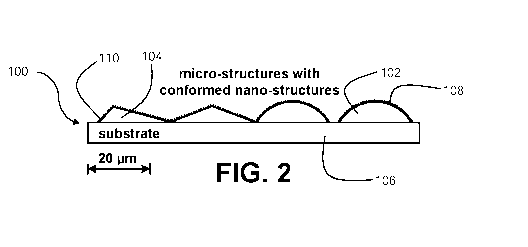
[0017] FIG. 2 is an illustrative depiction of an optical device comprising
micro-
structures with nano-structures conformed thereon.
[0018] FIGS. 3(a) and 3(b) are illustrative depictions of plasmonic
optical devices.
[0019] FIG. 4 is an illustrative depiction of another optical device
comprising
micro-structures with plasmonic pixels, which produces optical effects
different from
those in FIG. 3.
- 5 -
CA 03088210 2020-07-10
WO 2019/140527
PCT/CA2019/050065
[0020] FIG. 5 is an illustrative depiction of another optical device
comprising
micro-structures with plasmonic pixels, which produces optical effects
different from
those in FIG. 3 and FIG. 4.
[0021] FIG. 6 is an illustrative depiction of another optical device
comprising
micro-structures with plasmonic pixels, which produces optical effects
different from
those in FIG. 3, FIG. 4, and FIG. 5.
[0022] FIG. 7(a) and 7(b) include illustrative depictions of incident
light interacting
with diffracting surfaces.
[0023] FIG. 8 includes an illustrative depiction of incident light
interacting with
another embodiment of diffracting surfaces.
[0024] FIG. 9 includes magnified images of actual devices that include
micro-
structures and plasmonic nano-structures.
[0025] FIG. 10 includes images of a device that includes micro-structures
and
plasmonic nano-structures.
[0026] FIG. 11 is a magnified image of the device depicted in FIG. 10.
[0027] FIG. 12 is an image of a devices that include micro-structures and
diffractive nano-structures.
[0028] FIG. 13 includes magnified images of actual devices that include
micro-
structures and plasmonic nano-structures.
DETAILED DESCRIPTION
[0029] FIG. 1 illustrates various general aspects of relevant prior art
optical
devices, on approximately the same size scale. FIG. 1(a) depicts a
conventional micro-
optical device 10 that uses micro-lenses 12 to image micro-ink prints 14 to a
user that
observes the device from the top. The micro-ink prints are placed at a
distance from the
lenses by using a transparent spacer layer 16. Light reflected off inks and
physically
coupled to the spacer is transmitted through the spacer and through the micro-
lenses.
FIG. 1(b) depicts another conventional micro-optical device 20 that uses micro-
mirrors
22 placed on a substrate 24 to display a visual content to a user that
observes the
device from the top. Both of the devices of FIG. 1(a) and (b) work based on
light
reflection and refraction. FIG. 1(c) depicts another conventional device 30
that includes
one or more thin film layers 32 placed on a substrate 34. The device works
based on
optical interference effects. FIG. 1(d) depicts another conventional device 40
that
- 6 -
CA 03088210 2020-07-10
WO 2019/140527 PCT/CA2019/050065
includes micro- or nano-textures 42 placed on a substrate 44. The device may
work
based on variety of optical effects like diffraction, plasmonic (such as those
produced by
plasmonic structures and materials), photonic (such as those produced by
photonic
crystals), optical guides, and optical antennas, among others. The sizes of
the devices
depicted in FIG. 1 are rough approximates, and the figure is not meant to
describe a
specific device. However, FIG. 1 illustrates and compares the typical range of
prior art
device structural features that work based on different physics described
above. FIG. 1
is an illustration of the core optical elements; and in practice, the depicted
devices may
have additional layers (e.g. protective lacquers, adhesives, release layers,
or others).
[0030] The core element of micro-lens and micro-mirror devices on FIG. 1(a)
and
(b) are non-flat, that is they have substantial thickness variation that
extents above the
spacer or the substrate. Though the thickness variation may be only a matter
of a few
microns, it is this thickness variation that enables the optical function of
the devices. In
comparison, the thin films of the devices of FIG. 1(c) and the surface of the
devices of
FIG. 1(d) are substantially close to flat. Therefore, it is clear that the
prior art devices
depicted in FIG. 1 can be divided into two structural categories. In the first
category are
the devices in which the functional element is a non-flat surface with
thickness variation
of a few microns or more (e.g. those depicted in FIG. 1(a) and (b)). Such
devices do not
contain any additional micro- or nano- textures like that of FIG. 1(d),In the
second
category are the devices in which the functional element is flat or close to
flat (e.g. those
depicted in FIG. 1(c) and 1(d)). Such devices do not have any thickness
variations of a
few microns or more. The optical devices described below, similar to the first
category,
may have a non-flat core functional element with height variations of a few
microns or
more. However, they also include submicron sized features, similar to the
second
category. In all of the devices described here, the spacers or substrates
define a plane
for the device (the plane may be but need not be strictly planar; the plane
may be
substantially a plane, with a bend or curvature perceivable on a larger
scale).
[0031] FIG. 2 shows a schematic of an optical device 100 in accordance with
an
embodiment of the invention on the same size scale as FIG. 1. The sizes are
rough
approximates and the figure is not meant to describe a specific device design
for a
specific application. FIG. 2 helps demonstrate some structural differences of
the
disclosed invention in comparison to prior art optical devices depicted in
FIG. 1. The
optical device of FIG. 2 includes both micro- and nano-structures spread over
the
functional surface of the device. Specifically, micro-structures of two
different shapes
- 7 -
CA 03088210 2020-07-10
WO 2019/140527
PCT/CA2019/050065
102, 104 are shown provided on a substrate 106. (In the following the term
"substrate"
will be used to also include spacer layers as described above and more
generally any
structure on which optical structures may be formed or supported, directly or
indirectly.)
The micro-structures have surfaces ("micro-surfaces") on which nano-structures
108,
110 are formed. In one aspect the device of FIG. 2 is superficially similar to
the devices
of FIG. 1(a) and 1(b): both have a non-flat functional element with height
variations of a
few microns or more. In another aspect the device of FIG. 2 is superficially
similar to the
devices of FIG. 1(d): both have a functional element that includes sub-micron
features.
However, as described below, the structure, physics and optical function of
the device
of FIG. 2 fits neither of the prior art device categories. The final device
may include
structures not depicted in FIG. 2, such as additional layers like protective
layers,
adhesive layers, index matching layers, or others; but the main function of
the device
will be determined by a functional element similar to the one depicted in FIG.
2.
[0032] A few examples of the envisioned optical effects realizable with the
disclosed optical structures is described below. These should be regarded as
exemplar
functions the structures can offer, and the examples are not meant to place
any
restriction on the optical effects/functions such structures may offer in
future. In the
descriptions below, scales of structures are important. On a large scale, the
devices
resemble planar structures, with the micro- and nano-structures not being
readily visible
to the naked eye. On this scale, the devices may appear planar (although the
devices
may be flexible and may be subject to bending) and as used in the following
claims the
term "planar" or "generally planar" refers to such large scale characteristic
unless
otherwise specified. On a smaller scale, the micro-structures are visible
(typically with
some magnification instrument). Many of the micro-structures described below
are not
planar at this scale, but are three-dimensional. Exemplary sizes and shapes of
such
micro-structures are described below, but in general, the layer of micro-
structures has a
thickness less than 50 pm and more than 1 pm. On a still smaller scale, nano-
structures
(such as nano-holes, nano-columns, nano-slits, nano-disks, etc.) become
visible. Such
nano-structures themselves are three-dimensional. Nano-structures are
conformal to
the micro-structures, and therefore follow the contours of the micro-
structures. The
nano-structures may conform to all or portions of the micro-surface,
continuously or in a
piecewise manner, in accordance with the specific embodiment and application.
Exemplary sizes and shapes of such nano-structures are described below, but in
general, the nano-structures have at least one feature size smaller than 500
nm.
- 8 -
CA 03088210 2020-07-10
WO 2019/140527 PCT/CA2019/050065
[0033] FIG. 3(b) illustrates an embodiment of the invention employing
plasmonic
nano-structures 108 conformed to micro-structures 102, and FIG. 3(a)
illustrates what
may happen when visible incident light interacts with a flat plasmonic
surface. A
plasmonic surface is typically made of an arrangement of metallic nano-
particles, nano-
perforations, or nano-antennae in a thin metallic film (thickness <0.3 pm).
The
arrangement maybe periodic with any unit cell shape, or may be aperiodic.
Particles or
perforations may have any three-dimensional shape with minimum feature sizes
of 0.5
pm or less. The metal may be aluminum, gold, silver, copper, chromium, nickel,
or any
metal or metal-alloy with good enough specifications for plasmonic
applications. The
typical average distance between such particles or perforations may be in a
range less
than the wavelength of incident light (less than -1.0 pm). For these range of
dimensions, and for appropriately designed structures, the plasmonic surface
can act
more as a mirror-like filter than a planar diffractive surface. That is the
incident light is
absorbed, transmitted, or reflected through excitation of plasmons, and this
phenomena
takes place more efficiently than diffraction. This description outlines what
defines
'plasmonic surface' throughout this document.
[0034] Because the excitation of plasmons, their properties, and also
emission of
light from them are all wavelength-dependent, reflected and transmitted
visible white
light from a plasmonic surface takes a color and an intensity. Depending on
the design
(or geometry or surface structures or materials) of the plasmonic surface,
both the color
and the intensity are changed. A large surface can be divided into many pixels
each
colored differently with utilization of different plasmonic structures to
display a visually
observable content in reflection and/or in transmission. This approach of
displaying
content on a plasmonic surface has been reported mostly in academic
publications
(e.g., see Shawn J. Tan et al, Plasmonic Color Palettes for Photorealistic
Printing with
Aluminum Nanostructures, Nano Letters, v14, p4023, 2014). A common feature of
all
such reports so far is that they are flat plasmonic surfaces. That is, they
are structurally
similar to devices depicted in FIG. 1(d) or FIG. 3(a).
[0035] Reflection from a flat plasmonic surface may be specular (i.e.
mirror-like -
see FIG. 3(a)). A large planar plasmonic surface thus appears much as a
mirror: it
appears too dark when it does not directly reflect the incident light to the
observer's
eyes, and appears too bright when it directly reflects the incident light to
the observer's
eyes. This mirror-like character is very unpleasant for observation of
plasmonic contents
described above; and it renders application of such contents practically
difficult. This is
- 9 -
CA 03088210 2020-07-10
WO 2019/140527
PCT/CA2019/050065
especially true for reflective plasmonic displays. The best reflective
displays like
traditional paper and inks should have a diffuse character, otherwise they
appear too
glossy for easy use.
[0036] An embodiment of the present invention addresses this issue. FIG.
3(b)
shows the structure. Here, the plasmonic surface is made conformal to a micro-
surface,
the micro-surface corresponding to one or more non-flat micro-structures 102,
in
contrast with a plasmonic surface made on a flat or planar substrate as shown
in FIG.
3(a). Throughout this document, a 'micro-surface' refers generally to a layer
of micro-
structures with a thickness less than 50 pm and more than 1 pm. Examples of
two
different micro-surfaces are depicted in FIG. 2 which correspond to the
surfaces of
micro-structures 102, 104. In the device of FIG. 3(b), the color generation
mechanism is
through the working of a plasmonic surface, but the viewing angles of the
plasmonic
content are determined by the design of the micro-surface. For the specific
example of
FIG. 3(b), the function of the micro-surface is to spread the reflected lights
over a large
spread of angles to convert the mirror-like reflection from a flat plasmonic
surface into a
more diffuse type of reflection. Therefore, by tuning the micro-surface, this
embodiment
enables use of plasmonic colors to create displays with a desired level of
luster. In this
device, modification of the design of micro-surface can lead to plasmonic
devices with
an appearance similar to other, more ordinary objects such as printed inks on
paper
surfaces, different types of dyes or paints (e.g., flat, semi-gloss, gloss,
metallic, and
others), different types of colored transparent surfaces, similar to stained
glass (e.g.
transparent, matte, and others), different types of slides (e.g. transparent,
matte, and
others), or others. The optical function of the micro-surface may be
accurately designed
by using commercially available ray tracing software. In general the smoother
(rougher)
the surface, the glossier (more matte) the final device is expected to be. In
the same
device, modifications of plasmonic structures can lead to plasmonic devices to
display
different contents useful for different applications. Most of the
illustrations herein are
two-dimensional cross-sections of the device structures. The micro-surface for
the
actual devices may take any arbitrary convex or concave three-dimensional
shape that
falls within the specified dimensions. FIG. 3(b) illustrates an embodiment of
micro-
surfaces having arcuate cross-sectional shape. These may correspond to three-
dimensional shapes which are cylindrical or have repeating dome shapes or
sections of
spherical shapes. Various other arcuate surfaces are possible.
[0037] Another embodiment of the present invention is depicted in FIG. 4.
In this
- 10 -
CA 03088210 2020-07-10
WO 2019/140527 PCT/CA2019/050065
embodiment, the micro-surface is shaped into a pyramidal shape (e.g. a
pyramid, a
wedge, or a triangular prism). A plasmonic surface 112 with pixels providing
content of
image #1 is made conformal to one face of the pyramids, and a second plasmonic
surface 114 with pixels providing content of image #2 is made conformal to the
other
face of the pyramids. Specular reflection of the incident light from the two
faces of the
pyramids reveals content of image #1 viewable by observer #1, and content of
image #2
viewable by observer #2. The device affixed to a document or product,
therefore,
appears to an observer as a switch from image #1 to image #2, enabled by tilt
of the
sample (or otherwise changing point of view or changing the direction of
incident light).
Image #2 maybe left blank, and the result will be a device that displays image
#1 turning
on and off with tilt of the sample. Faces for images #1 and #2 maybe uniformly
patterned with two different types of plasmonic structures, and the result
will be a device
that displays plasmonic color #1 which switches to plasmonic color #2. The two
observers may be two eyes of a single observer; the plasmonic content may
contain two
perspectives of a single scene/object; and in such case the device creates an
illusion of
depth similar to that of present three-dimensional televisions or theaters.
The number of
encoded images and their observation angles can be selected by designing the
employed micro-surface. The displayed contents can be selected by utilization
of
appropriate plasmonic surface conformed to the micro-surface. The present
invention
and the resulting platform described in this embodiment is capable of yielding
optical
effects with strong asymmetries; and as such effects are rarely possible with
other
techniques, the devices are useful to function as optical anti-counterfeiting
security
features.
[0038] Another embodiment of the present invention is depicted in FIG. 5.
Here
the micro-surface has at least three flat faces (e.g., a frustum or truncated
pyramid). A
plasmonic surface 118 with pixels providing content of image #1 is made
conformal to
one face, a second plasmonic surface 120 with pixels providing content of
image #2 is
made conformal to the second face, and a third plasmonic surface 122 with
pixels
providing content of image #3 is made conformal to the third face. Specular
reflection of
the incident light from the three faces reveals contents of image #1 to image
#3
viewable by observer #1 to #3. The device affixed to a document or product,
therefore,
appears to an observer as a switch from image #1 to image #3 enabled by tilt
of the
sample.
[0039] As suggested by FIG. 4 and FIG. 5, the number of faces of the micro-
-11 -
CA 03088210 2020-07-10
WO 2019/140527
PCT/CA2019/050065
surface can be expanded. Consequently, the number of encoded images can be
increased through an increase in the number of faces of the micro-surface.
Increasing
the number of faces may result in a decrease in the size of pixels of the
corresponding
plasmonic surfaces. Each image of such high face density micro-surface can
hold a
frame of an animation; and the resulting sample can show an animation
displayed by tilt
of the sample. The animation may appear two dimensional or three dimensional
depending on the optical design of the micro-structures and nano-structures.
The micro-
surface for this embodiment can be a piecewise linear three-dimensional shape
to keep
the frame displays maximally separated, or a curved three-dimensional shape to
help
display of a smooth animation.
[0040] Another
embodiment of the present invention is illustrated in FIG. 6. The
device is structurally similar to that of FIG. 4, but the optical function is
different: the
observers¨instead of looking at the reflected light¨look at the transmitted
light.
Because the incident lights #1 and #2 pass through plasmonic pixels 124, 126
of image
#1 and #2, the observers #1 and #2 see the contents of image #1 and #2,
respectively.
The device affixed to a transparent planar substrate 128 and observed in
transmission,
therefore, appears to an observer as a switch from image #1 to image #2
enabled by tilt
of the sample. Such device maybe installed on a polymer banknote, on a
windowed
banknote, on a transparent tag attached to a product, or on other similar
materials to
protect them from counterfeiting activities. The number of encoded images and
their
observation angles can be selected by designing the employed micro-surface.
The
displayed contents can be selected by utilization of appropriate plasmonic
surface
conformed to the micro-surface. The contents can be anything from complex
imagery to
simple colors. The displayed content can be anything from simple color shifts
or
switches, to switches between complex imagery, to fluid animations.
[0041] FIG.
7(a) illustrates what may happen when incident light interacts with a
flat diffractive surface. Such surface can be made of an arrangement of
metallic or
dielectric nano-particles (or structures such as nano-columns) or nano-
perforations (or
nano-holes or pillars or gratings) in a thin metallic or dielectric film
(thickness <0.3 pm).
The arrangement of nano-structures can be periodic with any unit cell shape.
Particles
or perforations may have any three-dimensional shape with feature sizes of 1.0
pm or
less. The metal may be aluminum, gold, silver, copper, or any other metal. The
dielectric may be resin, plastic, 5i02, Nb2O5, TiO2, ZnS, or other materials
having a
refractive index different than that of the surrounding layers. The array
periodicity is
- 12 -
CA 03088210 2020-07-10
WO 2019/140527
PCT/CA2019/050065
close to the range of the wavelength of incident light (more than -0.3 pm and
less than
-1.0 pm). All the particles/perforations that make an array may be identical
in shape, or
they may have different shapes and sizes. For these range of dimensions, and
for
appropriately designed structures, the diffractive surface disperses the
spectrum of the
incident visible light into rainbow-like spectrums (that is, diffraction
orders, one of which
is shown in FIG. 7(a)). This description outlines what defines 'diffractive
surface'
throughout this document.
[0042] Because a flat diffractive surface disperses the incident light
into its
spectrum content, the surface appears colorful to an observer at an
appropriate fixed
angle. For particular incident and observation angles, the perceived color
depends on
the design (or geometry) of the diffractive surface. A large diffractive
surface can be
divided into many pixels each filled with a different diffractive structure.
Such surface
can display different contents ranging from monochromatic single images to
full color
three-dimensional ones. The color of such images depends on the observation
and
incident light angles. Such devices either through display of color changes
with tilt of the
sample, or through display of image switches, or through display of three-
dimensional
imagery or other visual effects find applications for optical anti-
counterfeiting devices.
For a flat diffractive surface (e.g., one having no micro-structures like that
of FIG. 1(a)
and 1(b)) under a fixed incident light, tuning the diffraction angles
generally requires
changing the design of diffracting nano- or micro-structures.
[0043] Another embodiment of the present invention is shown in FIG. 7(b).
Here,
the diffractive surface is made conformal to a micro-surface, the micro-
surface having
one or more micro-structures. The optical effects that may be obtained with
the device
depicted in FIG. 7(b) are in contrast with the optical effects that may be
obtained with
the device depicted in in FIG. 7(a). In the device depicted in FIG. 7(b), the
color
generation mechanism is through the working of a diffractive surface, but the
viewing
angles of the diffractive content is determined by both the design of the
micro-surface
and that of diffractive surface. For the specific example of FIG. 7(b), the
micro-surface
offers two flat faces. Pixels of image #1 are made by making the corresponding
diffractive surface 130 conformal to face #1, and pixels of image #2 are made
by a
second diffractive surface 132 conformal to face #2. The angles the two faces
make
with the planar substrate 134 provide degrees of freedom, using which the
contents of
the two diffractive faces can be spatially separated. Therefore, observer #1
sees the
content of image #1, and observer #2 sees the content of image #2.
Colloquially, two
- 13 -
CA 03088210 2020-07-10
WO 2019/140527
PCT/CA2019/050065
observers looking at the device at the same time under the same lighting
conditions
may see two distinct images with distinct colors. The device affixed to a
document or
product, therefore, appears to an observer as a switch from image #1 to image
#2
enabled by tilt of the sample. The number of encoded images and their
observation
angles can be changed through the design of an appropriate three-dimensional
micro-
surface and the diffractive surface conformal to it. The device may display
discrete
switches between diffractive contents, animations, three-dimensional contents,
or a
combination of these optical effects.
[0044] Another embodiment of the present invention is depicted in FIG. 8.
Here,
the diffractive surface 140 is made conformal to a micro-surface 142 formed on
substrate 138 with appropriate design to heavily spread the diffracted rays.
The
diffracted light therefore appears as a diffused light rather than specular as
that shown
in FIG. 7(a). Compared to present flat diffractive surface devices (such as
that of FIG.
7(a)), the device of FIG. 8 displays a more diffused content. The device may
thus
appear as prints on normal paper but made by highlight markers, rather than
flashy as
normal flat diffractive surface devices may appear to be. Of special interest
for devices
of this embodiment are diffractive surfaces with periodicities between -0.3 pm
and 0.5
pm. For this range of periodicities, the spectrum of diffracted light may lack
red side of
the spectrum; and this helps device designers manage a diffused diffraction in
creation
of meaningful contents.
[0045] FIG. 9, including FIG. 9(a) and FIG. 9(b), is an example of an
actual
device made using the present invention. FIG. 9 shows a scanning electron
microscope
image of a master mold that holds a micro-surface 152 and a plasmonic surface
150
conformal to it. In this specific example, the material of the master mold is
silicon; the
micro-surface is designed as cylindrical cuts with the width 30 pm and height
of 4 pm;
and the plasmonic pixels are designed as hexagonal arrays 154 of nano-holes
156 with
periodicities less than 0.4 pm, hole dimeters less than 0.3 pm, and hole depth
of -0.15
pm. FIG. 9(b) is a zoomed-in (more magnified) scanning electron microscope
image of
the same master mold. In this size scale, the individual nano-holes and their
conformality with the micro-surface can be clearly seen.
[0046] The method of fabrication of the device of FIG. 9 can include micro-
and
nano-fabrication steps commonly known to those who are familiar with the
field.
Fabrication of the specific device of FIG. 9 starts with a polished silicon
wafer. The
wafer is cleaned from dust and contaminates like organic materials or others
that may
- 14 -
CA 03088210 2020-07-10
WO 2019/140527 PCT/CA2019/050065
exist on the surface. The cleaned wafer is coated with a thick layer of
electron beam
resist. The coated wafer is then exposed to the patterns of the micro-
structures using an
electron-beam lithography machine. A few more typical steps of baking and
development yields patterns of micro-structures in the resist coating the
silicon wafer.
This soft pattern is transferred to the hard silicon by using a dry etching
machine. A few
more steps of chemical cleaning and baking removes the extra resist and leaves
a
clean silicon wafer with patterns of the designed micro-structured surface on
it. This
wafer is then recoated with a thin layer of electron resist. The recoated
wafer is then
exposed to the patterns of plasmonic structures using an electron beam
lithography
machine. Further steps of development, baking, dry etching, and cleaning
results in
formation and transfer of plasmonic structures (nano-hole arrays in this case)
to the
micro-surface. These steps or modified steps similar to the ones described
here can
yield all the devices described herein.
[0047] The device of FIG. 9 is only a mold that contains a specific
designed
surface, but it does not contain other layers (e.g. metallic layer) to enable
a functional
plasmonic device. The photo of an exemplar functional device is shown in FIG.
10.
Here, the designed micro- and nano-structures after fabrication on a mold is
casted on a
different substrate, such as a plastic sheet, using an ultra-violet curable
resin. A thin
layer of aluminum is then deposited on the casted copy and the resulting
aluminum
coated casting is laminated with additional protective layers. Such casting or
embossing, coating, lamination, or other operations are typically available in
industrial
format which may be employed for large-scale production of the devices. FIG.
10(a)
shows a top view of the device, and FIG. 10(b) shows a tilt view. The device
has a width
of 8 mm. The phrase `NTS' and the oblique bars display two different colors,
as the
plasmonic pixels used to make them are different. The phrase `NTS' appears
fixed in
position with tilt of the sample, while the colored bars 158 appear to shift
their positions.
A photo of this sample under an optical microscope is shown in FIG. 11. The
micro-
surface consists of cylindrical cuts similar to the ones shown in FIG. 9. Each
image pixel
conformed to the micro-surface is divided into many subpixels. The sample
employs two
types of pixels. In pixel type 1, the plasmonic content of all the subpixels
is the same.
The optical effect is to display a spatially fixed but diffused content like
that of the
phrase `NTS'. In pixel type 2, the plasmonic content of all the subpixels is
not the same.
The optical effect in this case is to display moving colored bars. Such device
finds
significant use for optical anti-counterfeiting applications, for example. The
micro-
- 15 -
CA 03088210 2020-07-10
WO 2019/140527 PCT/CA2019/050065
surface for this embodiment is a curved three-dimensional shape to construct a
display
of moving bars with a very smooth movement appearance. The micro-surface can
be
replaced with a piecewise linear three-dimensional shape to display a more
discrete
movement.
[0048] Another illustrative device employing the present invention is shown
in
FIG. 12. The structure of the device is similar to that shown in FIG. 9.
However, the area
is divided into two parts 160, 162. In the top part 160, the micro-surface is
conformably
covered with one type of diffracting nano-structures, whereas in the bottom
part 162, the
micro-surface is conformably covered with another type of diffracting nano-
structures.
These nano-structures are similar to the ones shown in FIG. 9(b), but they
have larger
periodicities so the diffraction rather than plasmonic effects becomes
dominant. The
result is appearance of two diffused diffractive colors from the two regions
of the device.
In this specific example, the material of the master mold is silicon; the
micro-surface is
designed as convex half-cylindrical structure with the width 30 pm and height
of 3.5 pm,
and a length corresponding to the total width of the display area (e.g. 4 mm
to 10 cm);
and the diffracting pixels are designed as rectangular arrays of nano-holes
with
periodicities 0.4 pm and 0.5 pm, hole diameters less than 0.25 pm, and hole
depth of
-0.11 pm. What is shown on FIG. 12 is a UV casted copy of this master mold
which is
coated by -35nm of aluminum. From the viewing side, the micro-surface is
mirrored to a
concave shape and nano-structures appear as nano-pillars.
[0049] FIG. 13 is another example of an actual device made using the
present
invention. It shows an atomic force microscope image of a master mold that
holds a
micro-surface and a plasmonic surface conformal to it. In this specific
example, the
material of the master mold is nickel; the micro-surface is designed as
piecewise linear
spherical cuts with width of 40 pm and total height of 4 pm; and the plasmonic
pixels are
designed as arrays of nano-holes and nano-pillars with periodicities less than
0.3pm,
hole/pillar diameters less than 0.2 pm, hole depth of -0.2 pm, and hole height
of -0.2
pm. The presented three dimensional image clearly shows features of an
exemplary
specific embodiment of the present invention.
[0050] While preferable embodiments of the present invention have been
shown
and described herein, it will be obvious to those skilled in the art that such
embodiments
are provided by way of example only. Numerous variations, changes, and
substitutions
will now occur to those skilled in the art without departing from the
invention. It should
be understood that various alternatives to the embodiments specifically
described
- 16 -
CA 03088210 2020-07-10
WO 2019/140527
PCT/CA2019/050065
herein may be employed, including (but not limited to) varieties of geometries
of micro-
and nano-structures and employment of photonic, plasmonic and diffractive
structures.
[0051] The illustrative embodiments herein described are not intended to be
exhaustive or to limit the scope of the invention to the precise forms
disclosed. They are
chosen and described to explain the principles of the invention and their
application and
practical use. Many alterations and modifications are possible in the practice
of this
invention without departing from the scope of the invention, which is defined
by the
claims appended hereto.
- 17 -