Note: Descriptions are shown in the official language in which they were submitted.
CARRIER-TYPE PULSED EDDY CURRENT TESTING METHOD AND DEVICE
BACKGROUND
[Technical Field]
[0001] The disclosure relates to the technical field of non-destructive
testing, and more
particularly, to a carrier-type pulsed eddy current testing method and a
carrier-type pulsed eddy
current detection device.
[Description of Related Art]
[0002] In industries such as oil and gas, chemical engineering, electricity,
and heating, during
the long-term service, metal components such as natural gas pipelines and
pressure vessels are
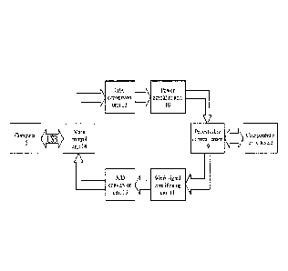
prone to large-area corrosion due to the influence of extreme temperature,
high pressure, and
complex external environment, as well as erosion and corrosion of the medium.
As a result,
cracking can arise and cause leakage or even explosion, which leads to huge
economic losses, and
causes great pollution and harms to the environment. The pulsed eddy current
testing technique
has the advantages of on-line testing, the ability of penetrate the cladding,
etc., and has broad
application in the detection of wall thinning of metal components. However,
due to the limitation
of acquisition accuracy, some extreme-sized metal components, such as thin
plates and small-
diameter pipes, are beyond the detection range of existing pulse eddy current
testing instruments,
which has become a major bottleneck restricting the development of this
technique.
[0003] Patent CN104849349A discloses a weld seam detection method for thin-
wall small-
diameter pipes. The method uses the combined technique of phased array
ultrasonic testing,
which can be used to detect weld seams on small-diameter pipes with wall
thicknesses greater than
or equal to 3.5 mm and less than or equal to 7 mm. The method produces no
radiation and no
pollution, besides, it is simple to operate, intuitive and easy to understand,
because the detection
-1-
CA 3089622 2020-08-05
results are displayed in the form of a three-dimensional image. Therefore, the
method is suitable
to detect weld seams on the thin-wall small-diameter pipes. However, similar
to conventional
ultrasonic testing, in this method, coupling agent is necessary during
testing, so the installation of
the sensor is much more difficult, resulting in the low testing efficiency. In
addition, this method
is not applicable to the detection of the component with coatings.
[0004] Chinese Standard GB/T 28705-2012 stipulates a pulsed eddy current
testing method for
detecting wall thinning caused by large-area corrosion without removing the
cover layer, which is
applicable to ferromagnetic components made of carbon steel and low alloy
steel with diameters
of no less than 50 mm, thicknesses of 3 mm to 65 mm and covered by insulations
with thicknesses
of 0 to 200 mm in a temperature of -150 C to 500 C. However, with regard to
thin plates with
thicknesses less than 3 mm or small-diameter pipes with diameters smaller than
50 mm, pulsed
eddy current testing signals attenuate quickly, leading to poor acquisition
accuracy. Therefore, this
method is invalid for these components.
SUMMARY
[0005] In view of the limitations of the above existing technology, the
disclosure provides a
carrier-type pulsed eddy current testing method and a carrier-type pulsed eddy
current testing
device. Specifically, a metal plate with high permeability or high
conductivity is mounted under
the pulsed eddy current sensor, named carrier plate in this patent. The pulsed
eddy current signals
are obtained by the sensor with the carrier plate. And then two signals are
respectively measured
with the metal component to be tested and without it. This method can solve
the problem that the
pulse eddy current testing signal of metal components such as thin plates and
small-diameter pipes
attenuates rapidly, so that signals of such components can be collected.
[0006] In order to achieve the above objective, an aspect of the disclosure
provides a carrier-
type pulsed eddy current testing method, including steps below.
-2-
CA 3089622 2020-08-05
[00071 Si: A metal plate is mounted under a pulsed eddy current sensor, and
square wave
excitation is applied to the pulsed eddy current sensor to receive an
attenuation curve, i.e., a carrier
signal, of an induced voltage in the pulsed eddy current sensor over time as
the square wave
excitation decreases.
[0008] S2: A metal component to be tested is placed under the pulsed eddy
current sensor
mounted with the metal plate, and square wave excitation is applied again to
the pulsed eddy
current sensor to receive an attenuation curve, i.e., a modulating signal, of
an induced voltage in
the pulsed eddy current sensor over time as the square wave excitation
decreases.
[0009] S3: The carrier signal and the modulating signal are demodulated to
obtain the pulsed
eddy current testing signal of the metal part to be tested, and based on the
original pulsed eddy
current testing signal, a wall thickness or defect detection of the metal part
to be tested can be
realized.
[0010] Preferably, the metal component to be tested is a thin plate with a
thickness of 2 mm to
40 mm or a pipe with a diameter greater than 25 mm.
[0011] Preferably, the square wave excitation in S1 and S2 is 0.1 A to 5 A.
[0012] Another aspect of the disclosure provides a carrier-type pulsed eddy
current testing
device for implementing the method, including a pulsed eddy current sensor, an
external control
unit, and a metal plate. The pulsed eddy current sensor is configured to
induce the induced
voltage when subjected to square wave excitation. The external control unit is
connected to the
pulsed eddy current sensor and is configured to provide the square wave
excitation to the pulsed
eddy current sensor and receive the induced voltage signal from the pulsed
eddy current sensor.
The metal plate is mounted under the pulsed eddy current sensor.
[0013] Preferably, the pulsed eddy current sensor includes a sensor cover, an
aviation connector,
a driver coil, a pickup coil, and a sensor base. The sensor cover is mounted
on the sensor base.
The aviation connector is fixed on the sensor cover and is connected to the
external control unit.
-3-
CA 3089622 2020-08-05
The driver coil and the pickup coil are both fixed on the sensor base and are
connected to the
aviation connector.
[0014] Preferably, the external control unit includes a computer, a main
control unit, a D/A
conversion unit, an A/D conversion unit, a power amplifier unit, and a weak
signal conditioning
unit. The computer is connected to the main control unit. The main control
unit is connected
to the D/A conversion unit and the A/D conversion unit. The D/A conversion
unit is connected
to the power amplifier unit. The A/D conversion unit is connected to the weak
signal
conditioning unit. The power amplifier unit and the weak signal conditioning
unit are both
connected to the pulsed eddy current sensor.
[0015] At the time of test, a square wave signal generated by the computer is
transmitted to the
D/A conversion unit via the main control unit. The D/A conversion unit
converts the square
wave signal into an analog signal and transmits it to the power amplifier
unit. The power
amplifier unit converts the analog signal into square wave excitation and
provides it to the pulsed
eddy current sensor. The pulsed eddy current sensor generates an induced
voltage due to action
of the square wave excitation. The weak signal conditioning unit obtains the
induced voltage
signal, amplifies and filters it, and transmits it to the A/D conversion unit.
The A/D conversion
unit converts the amplified and filtered induced voltage signal into a digital
signal and transmits
it to the computer via the main control unit. The computer processes the
digital signal to obtain
relevant information.
[0016] Preferably, the metal plate is made of a highly magnetically conductive
or highly
electrically conductive material.
[0017] Preferably, a thickness of the metal plate is 1 mm to 20 mm.
[0018] Generally, compared with the existing technology, the above technical
solutions
conceived in the disclosure mainly have the following technical advantages.
[0019] 1. In the disclosure, a metal plate is adopted to obtain a carrier
signal, and a pulsed eddy
-4-
CA 3089622 2020-08-05
current testing signal of a metal component to be tested is obtained through a
demodulation
method, which solves the problem that it is difficult to effectively collect
the signal of metal
components such as thin plates and small-diameter pipes due to excessively
rapid attenuation, and
expands the application scope of pulsed eddy current testing.
[0020] 2. The disclosure reduces the requirements for signal acquisition
precision and speed,
and thus can simplify the pulsed eddy current testing device.
[0021] 3. The disclosure adopts a highly magnetically conductive or highly
electrically
conductive material to make the metal plate, and the eddy current is
attenuated slowly in the metal
plate, which reduces the attenuation rate of the obtained signal and is
beneficial for signal
collection.
BRIEF DESCRIPTION OF THE DRAWINGS
[0022] FIG. 1 is a schematic view showing a magnetic field distribution at the
time of pulsed
eddy current testing according to an embodiment of the disclosure.
[0023] FIG. 2 is an overall structural view showing a carrier-type pulsed eddy
current testing
device according to an embodiment of the disclosure.
[0024] FIG. 3 is a schematic structural view showing a pulsed eddy current
sensor according to
an embodiment of the disclosure.
[0025] FIG. 4 is a waveform diagram showing a carrier signal and a modulating
signal when a
small-diameter pipe is tested according to an embodiment of the disclosure.
[0026] FIG. 5 is diagram showing a waveform of an pulsed eddy current testing
signal of a
small-diameter pipe measured in an embodiment of the disclosure and a
comparison waveform.
[0027] In all the drawings, the same reference numerals are used to denote the
same elements
or structures: 1- screw, 2- sensor cover, 3- sensor base, 4- pickup coil, 5-
aviation connector, 6-
driver coil, 7- metal plate, 8- metal component to be tested, 9- pulsed eddy
current sensor, 10-
-5-
CA 3089622 2020-08-05
power amplifier unit, 11- weak signal conditioning unit, 12- D/A conversion
unit , 13- AID
conversion unit, 14- main control unit, 15-computer.
DESCRIPTION OF THE EMBODIMENTS
[0028] To provide a further understanding of the objectives, technical
solutions, and advantages
of the disclosure, the disclosure will be further described in detail below
with reference to the
accompanying drawings and the embodiments. It should be understood that the
specific
embodiments described herein are only used to interpret the disclosure and are
not intended to
limit the disclosure. In addition, the technical features involved in the
various embodiments of
the disclosure described below can be combined with each other as long as
there is no conflict
with each other.
[0029] A carrier-type pulsed eddy current testing method provided in an
embodiment of the
disclosure includes the following steps.
[0030] Si: A metal plate 7 is mounted under a pulsed eddy current sensor 9,
and square wave
excitation is applied to a driver coil 6 in the pulsed eddy current sensor 9.
The excitation current
generates a changing magnetic field in space, as shown in FIG. 1. Thus, an
eddy current is
induced in the metal plate 7, and the eddy current also generates a
corresponding magnetic field.
The above two magnetic fields form a superimposed magnetic field, and a pickup
coil 4 receives
an attenuation curve, i.e., a carrier signal, of the induced voltage generated
by the superimposed
magnetic field over time as the square wave excitation decreases.
[0031] S2: A metal component 8 to be tested is placed under the pulsed eddy
current sensor 9
mounted with the metal plate 7, and square wave excitation is applied to the
driver coil 6. The
excitation current generates a changing magnetic field in space. eddy currents
are induced in
both the metal plate 7 and the metal component 8 to be tested, and the eddy
currents also generate
corresponding magnetic fields. The magnetic fields of the driver coil 6, the
metal plate 7, and
-6-
CA 3089622 2020-08-05
=
the metal component 8 to be tested together form a superimposed magnetic
field. The pickup
coil 4 receives an attenuation curve, i.e., a modulating signal, of the
induced voltage generated by
the superimposed magnetic field over time as the square wave excitation
decreases.
[0032] S3: A finite difference operation is performed between the obtained
modulating signal
and the obtained carrier signal (i.e. using the obtained modulating signal to
minus the obtained
carrier signal) for demodulation to obtain an original pulsed eddy current
testing signal of the
metal component 8 to be tested, and based on the original pulsed eddy current
testing signal, a
wall thickness or defect detection of the metal component 8 to be tested can
be realized.
Specifically, wall thickness measurement can be realized by extracting the
signal feature of the
late signal attenuation rate, and a component defect can be detected by
performing differentiation
with the signal of a defect-free region.
[0033] Specifically, the square wave excitation is 0.1 A to 5 A, and the
applicable metal
component 8 to be tested is a thin plate with a thickness of 2 mm to 40 mm or
a pipe with a
diameter greater than 25 mm.
[0034] The above method is implemented by a carrier-type pulsed eddy current
testing device,
which includes a pulsed eddy current sensor 9, a metal plate 7, and an
external control unit.
[0035] As shown in FIG. 3, the pulsed eddy current sensor 9 includes a sensor
cover 2, an
aviation connector 5, a driver coil 6, a pickup coil 4, and a sensor base 3.
The sensor cover 2 is
fixed on the sensor base 3 by screws I. The aviation connector 5 is mounted in
a mounting hole
of the sensor cover 2 and is connected to the external control unit. The
driver coil 6 and the
pickup coil 4 are both located inside the sensor base 3, are positioned by a
mandrel, and are
connected to the aviation connector 5. The lower part of the sensor base 3 is
provided with a
slot, and the metal plate 7 is mounted under the sensor base 3 through the
slot.
[0036] As shown in FIG. 2, the external control unit includes a computer 15, a
main control unit
14, a D/A conversion unit 12, an AID conversion unit 13, a power amplifier
unit 10, and a weak
signal conditioning unit 11. The computer 15 is connected to the main control
unit 14. The
-7-
CA 3089622 2022-11-24
=
main control unit 14 is connected to the D/A conversion unit 12 and the A/D
conversion unit 13.
The D/A conversion unit 12 is connected to the power amplifier unit 10. The
A/D conversion
unit 13 is connected to the weak signal conditioning unit 11. The power
amplifier unit 10 and
the weak signal conditioning unit 11 are both connected to the pulsed eddy
current sensor 9.
[0037] At the time of test, a square wave signal generated by the computer 15
is transmitted to
the D/A conversion unit 12 via the main control unit 14 through the USB
protocol. The D/A
conversion unit 12 converts the square wave signal into an analog signal and
transmits it to the
power amplifier unit 10. The power amplifier unit 10 converts the analog
signal into square wave
excitation and provides it to the pulsed eddy current sensor 9. Due to the
action of the square
wave excitation, the pulsed eddy current sensor 9 generates an induced
voltage. The weak signal
conditioning unit 11 obtains the induced voltage signal, amplifies and filters
it, and transmits it to
the A/D conversion unit 13. The A/D conversion unit 13 converts the amplified
and filtered
induced voltage signal into a digital signal and transmits it to the computer
15 via the main control
unit 14. The computer 15 processes the digital signal to obtain relevant
information.
[0038] Further, the metal plate 7 is made of a highly magnetically conductive
or highly
electrically conductive material, such as #45 steel or aluminum, and the
thickness of the metal
plate 7 is 1 mm to 20 mm.
[0039] A specific example will be described below.
[0040] Example 1
[0041] A pulsed eddy current testing signal of a small-diameter pipe made of
304 stainless steel,
with an outer diameter of 50 mm and a wall thickness of 10 mm, was obtained
through the above
device, and the adopted metal plate was an aluminum plate with a thickness of
6 mm.
[0042] The aluminum plate was mounted under the pulsed eddy current sensor,
and square wave
excitation was applied to obtain a carrier signal. Then, the small-diameter
pipe was placed under
the pulsed eddy current sensor mounted with the aluminum plate, and square
wave excitation was
-8-
CA 3089622 2020-08-05
applied to obtain a modulating signal. The obtained carrier signal and the
obtained modulating
signal are as shown in FIG. 4, where the vertical axis represents the induced
voltage (V), and the
horizontal axis represents the time (s).
[0043] Differentiation was performed on the carrier signal and the modulating
signal to obtain
a modulated/demodulated signal, i.e., the pulsed eddy current testing signal
of the small-diameter
pipe, as shown in FIG. 5, where the vertical axis represents the induced
voltage (V), and the
horizontal axis represents the time (s). Meanwhile, FIG. 5 also shows an
original signal of the
small-diameter pipe obtained by the pulsed eddy current sensor without the
metal plate. It is
shown that due to the limitation of the acquisition speed of the device, the
early signal could not
be accurately obtained, and its attenuation pattern deviated greatly from the
theory. In contrast,
the signal obtained by the method of the disclosure basically conforms to the
theoretical
attenuation law and can be used for subsequent defect or wall thickness
analysis.
[0044] Those skilled in the art can easily understand that the above is only a
preferred
embodiment of the disclosure and is not intended to limit the disclosure. Any
modification,
equivalent replacement, and improvement made within the spirit and principle
of the disclosure
should be included in the protection scope of the disclosure.
-9-
CA 3089622 2020-08-05