Note: Descriptions are shown in the official language in which they were submitted.
CA 03089698 2020-07-27
WO 2019/150097 PCT/GB2019/050247
1
1 Injection-Locked Laser System
2
3 The present invention relates to the field of lasers and, in particular,
to a continuous-wave
4 (OW) injection-locked laser system.
6 Phase-locked laser systems are a known technique for actively phase
matching two
7 optical fields. However, these systems fail to provide a high degree of
phase-coherence at
8 high frequencies since such frequencies are beyond the frequency range at
which active
9 phase-control is feasible or easily achieved. Phase-locked laser systems
also suffer from
the effects of a "servo-bump" i.e. an amplification of phase-noise just beyond
the
11 frequency range of the active control system.
12
13 An alternative technique for phase matching two optical fields are those
based on
14 injection-locking. Injection-locking techniques are applied mainly to
continuous-wave
single-frequency laser sources. It is achieved by employing a low power laser
with
16 desirable frequency properties (the master laser) to impose its
frequency onto a higher
17 power laser (the slave laser) whose spectral properties would otherwise
not be as good.
18 Injection-locking is required because such low-noise performance, or
even just single-
19 frequency operation, is significantly more difficult to achieve in high-
power lasers, because
CA 03089698 2020-07-27
WO 2019/150097 PCT/GB2019/050247
2
1 these lasers tend to be more susceptible to mechanical vibrations, cannot
utilise very low-
2 noise pump sources, and are subject to significant thermal influences.
3
4 Injection-locking is achieved by injecting the output of the master laser
into the cavity of
the slave laser. As the frequency of the master laser approaches one of the
axial mode
6 frequencies of the slave laser, light from the master laser is
regeneratively amplified to
7 higher intensities, eventually saturating the gain in the slave laser to
such an extent that
8 the original free-running mode of the slave laser is extinguished. Within
this locking-range,
9 the output of the slave laser is phase locked to the phase of the output
of the master laser.
Injection-locking offers the advantage of single-frequency operation of a high-
power laser
11 without the use of etalons or other intracavity elements that would
reduce the power
12 efficiency, and which are often unable to tolerate the desired high
power levels.
13
14 US patent number US 5,027,360 discloses a high-power injection-locked
laser system that
comprises a master and a slave laser, both of which are solid state lasers
having
16 continuous wave outputs. In the disclosed system the slave laser has an
output power at
17 least ten times greater than the master laser. The system further
comprises a servo-loop
18 control system employed to maintain the injection-locked condition. This
is achieved by
19 generating an error signal that is indicative of fluctuations within the
slave laser cavity and
employing this error signal to adjust the length of the slave laser cavity to
maintain the
21 locked condition.
22
23 Frequency modulated lasers and mode-locked lasers have also been
employed as the
24 master laser to simultaneously injection-lock two or more slave lasers,
see for example US
patent numbers US 4,635,246 and US 5,379,309. In these systems different
optical
26 modes of the mode-locked master laser are employed to injection-lock
independent laser
27 oscillators. As a result, injection locking of two or more slave lasers
resonant at operating
28 frequencies of:
29
f = fo nAf (1)
31
32 where
33
34 fo is the central operating frequency of the master laser
n is an integer; and
CA 03089698 2020-07-27
WO 2019/150097 PCT/GB2019/050247
3
1 Af is the frequency difference between the adjacent modes of the master
laser
2
3 has been achieved. Since the phase fluctuations of the modes of the
master laser are
4 .. highly correlated then the phase fluctuations of the output of the two or
more slave lasers
are similarly highly correlated.
6
7 .. Although the above described injection-locking techniques result in the
output of the slave
8 lasers having a highly matched phase with the output of the master laser,
in practice this
9 phase matching is not perfect. Imperfect following of the slave lasers
means that there is
still some residual phase noise, particularly at low frequencies. In addition,
phase noise
11 can be introduced during the transmission of the optical fields on the
injection locked
12 .. systems.
13
14 Summary of Invention
16 It is therefore an object of an embodiment of the present invention to
obviate or at least
17 .. mitigate the foregoing disadvantages of the injection-locked laser
system known in the art.
18
19 It is a further object of an embodiment of the present invention to
provide an injection-
locked laser system wherein a continuous wave master laser is employed to
21 simultaneously injection lock two or more slave lasers.
22
23 .. A yet further object of an embodiment of the present invention is to
provide an injection-
24 locked laser system which exhibits reduced phase noise when compared
with those
.. injection-locked laser systems known in the art.
26
27 .. According to a first aspect of the present invention there is provided
an injection-locked
28 .. laser system comprising: a master laser that generates a continuous-wave
output field
29 having a frequency (f0);
.. one or more optical modulators employed to produce from the continuous-wave
output
31 field a first seed optical field having a first frequency (f1) and a
second seed optical field
32 having a second frequency (f2)
33 wherein the first seed optical field provides an input to injection lock
one or more optical
34 amplifiers at the first frequency (f1) and the second seed optical field
provides an input to
injection lock one or more optical amplifiers at the second frequency (f2).
CA 03089698 2020-07-27
WO 2019/150097 PCT/GB2019/050247
4
2 Since the first seed optical field and the second seed optical field are
produced from the
3 continuous-wave output field of the master laser then the output fields
of the one or more
4 optical amplifiers also exhibit a high phase-coherence with each other
and the continuous-
wave output field. This arrangement also ensures that any noise introduced by
the master
6 laser is common to the one or more optical amplifiers injection locked by
the first and
7 second seed optical fields.
8
9 Optionally the injection-locked laser system comprises N optical
modulators employed to
produce from the continuous-wave output field N seed optical fields having a
frequency (fN)
11
12 The first frequency (f1) preferably equals the frequency of the
continuous-wave output field
13 (fo) plus a modulation frequency (8,f1) introduced by the one or more
optical modulators.
14 Preferably the second frequency (f2) equals the frequency of the
continuous-wave output
field (fo) minus the modulation frequency (8,f2) introduced by the one or more
optical
16 modulators. The use of positive and negative frequency shifts means that
a relative
17 frequency offset of Afi + f2 can be achieved by imparting a first
frequency shift onto the
18 output fields the one or more optical amplifiers injection locked by the
first optical seed
19 field and a second frequency shift onto the output fields the one or
more optical amplifiers
injection locked by the second optical seed field.
21
22 Preferably the modulation frequency (AO introduced by the one or more
optical modulator
23 is between 0.1 and 40 GHz. Preferably the modulation frequency (AO
introduced by the
24 one or more optical modulator is around 6 GHz.
26 Preferably the one or more optical modulators comprises an electro-optic
modulator
27 (EOM). Alternatively, the one or more optical modulators comprises an
acoustic-optic
28 modulator (AOM).
29
Preferably the first seed optical field is mode-matched with the one or more
optical
31 amplifiers injection locked by the first seed optical field. In a
similar manner, it is
32 preferable for the second seed optical field to be mode-matched with the
one or more
33 optical amplifiers injection locked by the second seed optical field.
34
CA 03089698 2020-07-27
WO 2019/150097 PCT/GB2019/050247
1 Most preferably the injection-locked laser system further comprises one
or more frequency
2 lock control loops to frequency lock one or more of the optical
amplifiers to the first seed
3 field.
4
5 Most preferably the injection-locked laser system further comprises one
or more frequency
6 lock control loops to frequency lock one or more of the optical
amplifiers to the second
7 seed field.
8
9 Most preferably the injection-locked laser system further comprises a
first phase lock
control loop that provides a feedback signal to one of the one or more optical
modulators
11 that allows for an output field of a first optical amplifier to be phase
locked to the first seed
12 optical field.
13
14 Most preferably the first phase lock control loop comprises a first
detector arranged to
generate a first electrical beat signal from a first optical beat signal
generated from the
16 combined output field of the first optical amplifier and the continuous-
wave output field.
17
18 The first phase lock control loop may further comprise a reference
oscillator employed to
19 generate a first reference signal a having a frequency equal to a
frequency of the first
electrical beat signal.
21
22 Most preferably the first phase lock control loop further comprises a
first frequency mixer
23 employed to generate a first error signal from the first electrical beat
signal and the first
24 reference signal.
26 Preferably the first phase lock control loop further comprises a first
voltage-controlled
27 oscillator a control signal for which is generated from the first error
signal. Preferably an
28 output signal from the first voltage-controlled oscillator provides the
feedback signal for the
29 first optical modulator. Optionally the first phase lock control loop
further comprises a first
frequency synthesiser located between the first voltage-controlled oscillator
and the first
31 optical modulator.
32
33 Alternatively, the first phase lock control loop further comprises a
first voltage-controlled
34 phase shifter a control signal for which is generated from the first
error signal. Preferably
an input signal for the first voltage-controlled phase shifter is generated by
a first fixed
CA 03089698 2020-07-27
WO 2019/150097 PCT/GB2019/050247
6
1 frequency oscillator. Optionally the first phase lock control loop
further comprises a first
2 frequency synthesiser located between the first voltage-controlled phase
shifter and the
3 first optical modulator. Alternatively, the first phase lock control loop
further comprises a
4 first frequency synthesiser located between the first fixed frequency
oscillator and the first
voltage-controlled phase shifter.
6
7 In a further alternative, the first phase lock control loop further
comprises a first reference
8 oscillator employed to generate a first reference signal a having a first
frequency fA. The
9 first phase lock control loop further comprises a first Direct Digital
Synthesiser (DDS)
employed to generate a second reference signal a having a second frequency fB.
Most
11 preferably the first frequency fA equals the frequency of the first
electrical beat signal
12 minus the second frequency fB.
13
14 Most preferably the first phase lock control loop further comprises a
first frequency mixer
employed to generate a first intermediate frequency signal from the first
electrical beat
16 signal and the first reference signal fA.
17
18 Most preferably the first phase lock control loop further comprises a
second frequency
19 mixer employed to generate an error signal from the first intermediate
frequency signal
and the second reference signal fB.
21
22 Preferably the first phase lock control loop further comprises a first
voltage-controlled
23 oscillator a control signal for which is generated from the first error
signal.
24
Preferably the first Direct Digital Synthesiser (DDS) is further employed to
generate an
26 output signal.
27
28 Most preferably the first phase lock control loop further comprises a
third frequency mixer
29 employed to generate the feedback signal to one of the one or more
optical modulators
from an output signal from the first voltage-controlled oscillator and the
output signal of the
31 first DDS.
32
33 Most preferably the injection-locked laser system further comprises a
second phase lock
34 control loop that provides a feedback signal to one of the one or more
optical modulators
CA 03089698 2020-07-27
WO 2019/150097 PCT/GB2019/050247
7
1 that allows for an output field of a second optical amplifier to be phase
locked to the
2 second seed optical field.
3
4 Most preferably the second phase lock control loop comprises a second
detector arranged
to generate a second electrical beat signal from a second optical beat signal
generated
6 from the combined output field of the second optical amplifier and the
continuous-wave
7 output field.
8
9 Preferably the reference oscillator is employed to generate a second
reference signal
having a frequency equal to a frequency of the second electrical beat signal.
11
12 Most preferably the second phase lock control loop further comprises a
second frequency
13 mixer employed to generate a second error signal from the second
electrical beat signal
14 and the second reference signal.
16 Preferably the second phase lock control loop further comprises a second
voltage-
17 controlled oscillator a drive signal for which is generated from the
second error signal.
18 Preferably an output signal from the second voltage-controlled
oscillator provides the
19 feedback signal for the second optical modulator. Optionally the second
phase lock
control loop further comprises a second frequency synthesiser located between
the
21 second voltage-controlled oscillator and the second optical modulator.
22
23 Alternatively, the second phase lock control loop further comprises a
second voltage-
24 controlled phase shifter a control signal for which is generated from
the second error
signal. Preferably an input signal for the second voltage-controlled phase
shifter is
26 generated by a second fixed frequency oscillator. Optionally the second
phase lock
27 control loop further comprises a second frequency synthesiser located
between the
28 second voltage-controlled phase shifter and the second optical
modulator. Alternatively,
29 the second phase lock control loop further comprises a second frequency
synthesiser
located between the second fixed frequency oscillator and the second voltage-
controlled
31 phase shifter.
32
33 In a further alternative, the second phase lock control loop further
comprises a second
34 reference oscillator employed to generate a third reference signal a
having a third
frequency fc. The second phase lock control loop further comprises a second
Direct
CA 03089698 2020-07-27
WO 2019/150097 PCT/GB2019/050247
8
1 Digital Synthesiser (DDS) employed to generate a fourth reference signal
a having a fourth
2 frequency fp. Most preferably the third frequency fc equals the frequency
of the second
3 electrical beat signal minus the fourth frequency fp.
4
Most preferably the second phase lock control loop further comprises a fourth
frequency
6 mixer employed to generate a second intermediate frequency signal from
the second
7 electrical beat signal and the third reference signal fc.
8
9 Most preferably the second phase lock control loop further comprises a
fifth frequency
mixer employed to generate a second error signal from the second intermediate
frequency
11 signal and the fourth reference signal fp.
12
13 Preferably the second phase lock control loop further comprises a second
voltage-
14 controlled oscillator a control signal for which is generated from the
second error signal.
16 Preferably the second Direct Digital Synthesiser (DDS) is further
employed to generate an
17 output signal.
18
19 Most preferably the second phase lock control loop further comprises a
sixth frequency
mixer employed to generate the feedback signal to one of the one or more
optical
21 modulators from an output signal from the second voltage-controlled
oscillator and the
22 output signal of the second DDS.
23
24 Preferably the injection-locked laser system further comprises one or
more optical isolators
located between the master laser and the one or more optical amplifiers.
26
27 Optionally the injection-locked laser system further comprises one or
more frequency
28 doubling stages arranged to frequency double the one or more of the
output fields the one
29 or more optical amplifiers and or a component of the continuous-wave
output field. In this
embodiment it is preferable for the first and or second optical beat signals
to be generated
31 after one or more frequency doubling stages.
32
33 According to a second aspect of the present invention there is provided
a method for
34 injection-locking two or more optical amplifiers the method comprising:
- generating a continuous-wave output field having a frequency (f0);
CA 03089698 2020-07-27
WO 2019/150097 PCT/GB2019/050247
9
1 - optically modulating the continuous-wave output field to produce a
first seed optical
2 field having a first frequency (f1) and a second seed optical field
having a second
3 frequency (f2);
4 - employing the first seed optical field to injection lock one or more
optical amplifiers
at the first frequency (f1); and
6 - employing the second seed optical field to injection lock one or
more optical
7 amplifiers at the second frequency (f2).
8
9 Preferably the method for injection-locking two or more optical
amplifiers further comprises
mode-matching the first seed optical field with the one or more optical
amplifiers injection
11 locked by the first seed field. In a similar manner, the method for
injection-locking two or
12 more optical amplifiers further comprises mode-matching the second seed
optical field with
13 the one or more optical amplifiers injection locked by the second seed
field.
14
Most preferably the method for injection-locking two or more optical
amplifiers further
16 comprises frequency locking one or more of the optical amplifiers to the
first seed field.
17
18 Most preferably the method for injection-locking two or more optical
amplifiers further
19 comprises frequency locking one or more of the optical amplifiers to the
second seed field.
21 Most preferably the method for injection-locking two or more optical
amplifiers further
22 comprises generating a first feedback signal to the optically modulated
continuous-wave
23 output field to phase lock an output field of one of the optical
amplifiers to the first seed
24 optical field.
26 Most preferably generating the first feedback signal comprises
generating a first optical
27 beat signal from the combined output field of one of the optical
amplifier and the
28 continuous-wave output field.
29
Generating the first feedback signal preferably further comprises generating a
first
31 electrical beat signal from the first optical beat signal.
32
33 Generating the first feedback signal preferably further comprises
generating a first
34 reference signal having a frequency equal to a frequency of the first
electrical beat signal.
CA 03089698 2020-07-27
WO 2019/150097 PCT/GB2019/050247
1 Preferably generation of the first feedback signal further comprises
generating a first error
2 signal from the first electrical beat signal and the reference signal.
3
4 Preferably generation of the first feedback signal further comprises
employing the first
5 error signal to generate a control signal for a first voltage-controlled
oscillator. Preferably
6 an output signal from the first voltage-controlled oscillator provides
the first feedback signal
7 for the optical modulator. Optionally the frequency of the first feedback
signal is multiplied
8 before arriving at the optical modulator.
9
10 Alternatively, generation of the first feedback signal further comprises
employing the first
11 error signal to generate a control signal for a first voltage-controlled
phase shifter. Most
12 preferably a first fixed oscillator provides an input signal for the
first voltage-controlled
13 phase shifter. Preferably an output signal from the first voltage-
controlled phase shifter
14 provides the feedback signal for the optical modulator. Optionally the
frequency of the
feedback signal is multiplied before arriving at the optical modulator.
Alternatively, the
16 frequency of the input signal is multiplied before arriving at the first
voltage-controlled
17 phase shifter.
18
19 In a further alternative, generating the first feedback signal
preferably further comprises
generating a first reference signal having a frequency fA.
21
22 Generating the first feedback signal preferably further comprises
generating a second
23 reference signal having a frequency fB Most preferably the first
frequency fA equals the
24 frequency of the first electrical beat signal minus the second frequency
fB.
26 Generating the first feedback signal preferably further comprises
generating a first
27 intermediate frequency signal from the first electrical beat signal and
the first reference
28 signal fA.
29
Most preferably generating the first feedback signal preferably further
comprises
31 generating an error signal from the first intermediate frequency signal
and the second
32 reference signal fB.
33
34 Preferably generating the first feedback signal preferably further
comprises generating a
control signal for a first voltage-controlled oscillator from the first error
signal.
CA 03089698 2020-07-27
WO 2019/150097 PCT/GB2019/050247
11
1
2 Most preferably generating the first feedback signal preferably further
comprises frequency
3 mixing an output signal from the first voltage-controlled oscillator and
an output signal from
4 a first DDS.
6 Most preferably the method for injection-locking two or more optical
amplifiers further
7 comprises generating a second feedback signal to the optically modulated
continuous-
8 wave output field to phase lock an output field of one of the optical
amplifiers to the second
9 seed optical field.
11 Most preferably generating the second feedback signal comprises
generating a second
12 optical beat signal from the combined output field of one of the optical
amplifiers and the
13 continuous-wave output field.
14
Generating the second feedback signal preferably further comprises generating
a second
16 electrical beat signal from the second optical beat signal.
17
18 Generating the second feedback signal preferably further comprises
generating a second
19 reference signal having a frequency equal to a frequency of the second
electrical beat
signal.
21
22 Preferably generating the second feedback signal further comprises
generating a second
23 error signal from the second electrical beat signal and the second
reference signal.
24
Preferably generating the second feedback signal further comprises employing
the second
26 error signal to generate a control signal for a second voltage-
controlled oscillator.
27 Preferably an output signal from the second voltage-controlled
oscillator provides the
28 second feedback signal for the optical modulator. Optionally the
frequency of the second
29 feedback signal is multiplied before arriving at the optical modulator.
31 Alternatively, generating the second feedback signal further comprises
employing the
32 second error signal to generate a control signal for a second voltage-
controlled phase
33 shifter. Most preferably a second fixed oscillator provides an input
signal for the second
34 voltage-controlled phase shifter. Preferably an output signal from the
second voltage-
controlled phase shifter provides the feedback signal for the optical
modulator. Optionally
CA 03089698 2020-07-27
WO 2019/150097 PCT/GB2019/050247
12
1 the frequency of the feedback signal is multiplied before arriving at the
optical modulator.
2 Alternatively, the frequency of the input signal is multiplied before
arriving at the second
3 voltage-controlled phase shifter.
4
In a further alternative, generating the second feedback signal preferably
further comprises
6 generating a third reference signal having a frequency fc.
7
8 Generating the second feedback signal preferably further comprises
generating a fourth
9 reference signal having a frequency fp. Most preferably the third
frequency fc equals the
frequency of the second electrical beat signal minus the fourth frequency fp.
11
12 Generating the second feedback signal preferably further comprises
generating a second
13 intermediate frequency signal from the second electrical beat signal and
the third
14 reference signal fc.
16 Most preferably generating the second feedback signal preferably further
comprises
17 generating an error signal from the second intermediate frequency signal
and the fourth
18 reference signal fp.
19
Preferably generating the second feedback signal preferably further comprises
generating
21 a control signal for a second voltage-controlled oscillator from the
second error signal.
22
23 Most preferably generating the second feedback signal preferably further
comprises
24 frequency mixing an output signal from the second voltage-controlled
oscillator and an
output signal from a second DDS.
26
27 Preferably the method for injection-locking two or more optical
amplifiers further comprises
28 optically isolating the continuous-wave output field from the one or
more optical amplifiers.
29
Preferably the method for injection-locking two or more optical amplifiers
further comprises
31 frequency doubling one or more of the output fields the one or more
optical amplifiers and
32 or a component of the continuous-wave output field. In this embodiment
it is preferable to
33 generate the first and or second optical beat signals after frequency
doubling the one or
34 more of the output fields of the one or more optical amplifiers and or a
component of the
continuous-wave output field.
CA 03089698 2020-07-27
WO 2019/150097 PCT/GB2019/050247
13
1
2 Embodiments of the second aspect of the present invention may comprise
features to
3 implement the preferred or optional features of the first aspect of the
present invention or
4 vice versa.
6 According to a third aspect of the present invention there is provided an
injection-locked
7 laser system comprising: a master laser that generates a continuous-wave
output field
8 .. having a frequency (fo) and a first optical modulator employed to produce
from the
9 continuous-wave output field a first seed optical field having a first
frequency (f1), the first
seed optical field providing an input to injection lock a first optical
amplifier at the first
11 frequency (fl)
12 wherein the injection-locked laser system further comprises a first
phase lock control loop
13 that provides a feedback signal to the first optical modulator that
allows for an output field
14 of the first optical amplifier to be phase locked to the the first seed
optical field.
16 Preferably the injection-locked laser system further comprises a second
optical modulator
17 employed to produce from the continuous-wave output field a second seed
optical field
18 having a second frequency (f2). The second seed optical field may
provide an input to
19 injection lock a second optical amplifier at the second frequency (f2).
In this embodiment
the injection-locked laser system may further comprise a second phase lock
control loop
21 that provides a feedback signal to the second optical modulator that
allows for an output
22 field of the second optical amplifier to be phase locked to the the
second seed optical field.
23
24 Preferably the first seed optical field is mode-matched with the first
optical amplifier
injection locked by the first seed optical field. In a similar manner, it is
preferable for the
26 second seed optical field to be mode-matched with the second optical
amplifier injection
27 locked by the second seed optical field.
28
29 Most preferably the injection-locked laser system further comprises one
or more frequency
lock control loops to frequency lock a resonance condition of the first
optical amplifier to
31 the first seed optical field.
32
33 Most preferably the injection-locked laser system further comprises one
or more frequency
34 lock control loops to frequency lock a resonance condition of the second
optical amplifier
.. to the second seed optical field.
CA 03089698 2020-07-27
WO 2019/150097 PCT/GB2019/050247
14
1
2 Embodiments of the third aspect of the present invention may comprise
features to
3 implement the preferred or optional features of the first or second
aspects of the present
4 invention or vice versa.
6 According to a fourth aspect of the present invention there is provided a
method for
7 injection-locking an optical amplifier, the method comprising:
8 - generating a continuous-wave output field having a frequency (f0);
9 - optically modulating the continuous-wave output field to produce a
first seed optical
field having a first frequency (f1);
11 - employing the first seed optical field to injection lock a first
optical amplifier at the
12 first frequency (f1); and
13 - generating a feedback signal for the first optical modulator to phase
lock an output
14 field of the first optical amplifier to the the first seed optical
field.
16 Embodiments of the fourth aspect of the present invention may comprise
features to
17 implement the preferred or optional features of the first to third
aspects of the present
18 invention or vice versa.
19
According to a fifth aspect of the present invention there is provided an
injection-locked
21 laser system comprising: a master laser that generates a continuous-wave
output field
22 having a frequency (f0) and one or more optical modulators employed to
produce from the
23 continuous-wave output field one or more seed optical field having a
frequency (fN), the
24 one or more seed optical field providing an input to injection lock one
or more optical
amplifiers at the frequency (fN)
26 wherein the injection-locked laser system further comprises one or more
phase lock
27 control loops that provide one or more feedback signals to the one or
more optical
28 modulators that allows for an output field of the one or more optical
amplifiers to be phase
29 locked to the the one or more seed optical field.
31 Embodiments of the fifth aspect of the present invention may comprise
features to
32 implement the preferred or optional features of the first to fourth
aspects of the present
33 invention or vice versa.
34
CA 03089698 2020-07-27
WO 2019/150097 PCT/GB2019/050247
1 According to a sixth aspect of the present invention there is provided a
method for
2 injection-locking one or more optical amplifiers, the method comprising:
3 - generating a continuous-wave output field having a frequency (f0);
4 - optically modulating the continuous-wave output field to produce one
or more seed
5 optical fields having a first frequency (fN);
6 - employing the one or more seed optical fields to injection lock one
or more optical
7 amplifier at one or more frequencies (fN); and
8 - generating feedback signals for the one or more optical modulators
to phase lock
9 an output field of the one or more optical amplifiers to the the one or
more seed
10 optical fields.
11
12 Embodiments of the sixth aspect of the present invention may comprise
features to
13 implement the preferred or optional features of the first to fifth
aspects of the present
14 invention or vice versa.
16 Brief Description of Drawings
17
18 There will now be described, by way of example only, various embodiments
of the invention
19 with reference to the drawings, of which:
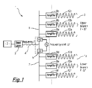
21 Figure 1 presents a schematic representation of an injection-locked
laser system in
22 accordance with an embodiment of the present invention;
23
24 Figure 2 presents a schematic representation of:
(a) an optical amplifier employed within the injection-locked laser systems of
Figure 1 and
26 (b) an alternative optical amplifier employed within the injection-
locked laser systems of
27 Figure 1;
28
29 Figure 3 presents a schematic representation of an injection-locked
laser system in
accordance with an alternative embodiment of the present invention;
31
32 Figure 4 presents a schematic representation of an injection-locked
laser system comprising
33 a phase lock;
34
CA 03089698 2020-07-27
WO 2019/150097 PCT/GB2019/050247
16
1 Figure 5 presents a schematic representation of an injection-locked laser
system comprising
2 an alternative phase lock;
3
4 Figure 6 presents a schematic representation of an injection-locked laser
system comprising
a second alternative phase lock; and
6
7 Figure 7 presents a schematic representation of an injection-locked laser
system comprising
8 a phase lock with a frequency chirp.
9
In the description which follows, like parts are marked throughout the
specification and
11 drawings with the same reference numerals. The drawings are not
necessarily to scale and
12 the proportions of certain parts have been exaggerated to better
illustrate details and
13 features of embodiments of the invention.
14
Detailed Description
16
17 Details of an injection-locked laser system will now be described with
reference to Figures
18 1. In particular, Figure 1 presents a schematic representation of an
injection-locked laser
19 system in accordance with a first embodiment of the present invention,
as generally
depicted by reference numeral 1.
21
22 The injection-locked laser system 1 can be seen to comprise a first
Ti:sapphire laser 2
23 employed as the master (or seed) laser within the system 1. The master
Ti:sapphire
24 lasers 2 is optically pumped at 532 nm by a dedicated continuous wave
diode-pumped
solid-state (DPSS) laser source 3 to produce a continuous-wave output field 4.
The
26 applicant's proprietary SolsTiS laser is a suitable example of a
Ti:sapphire laser for use
27 as the master laser 2 while the pump laser 3 may comprise a commercially
available
28 diode-pumped solid-state (DPSS) laser.
29
The pump laser 3 has the capability of providing up to 18 Watts of pump power
to the
31 master Ti:sapphire lasers 2. In the presently described embodiment, the
pump laser 3 is
32 arranged to provide -6 W of pump power to the master Ti:sapphire lasers
2 to provide a
33 tuneable continuous-wave output field 4 (tuneable between 700nm and
1000nm) with a
34 power of around 1 W at 780nm. With this arrangement the generated
tuneable
CA 03089698 2020-07-27
WO 2019/150097 PCT/GB2019/050247
17
1 continuous-wave output field 4 operates at a single frequency (f0), as a
single transverse
2 and longitudinal mode and exhibits low phase noise.
3
4 The continuous-wave output field 4 is then directed towards an optical
modulator 5. The
function of the optical modulator 5 is to produce first 6 and second 7 seed
optical fields
6 from the continuous-wave output field 4. The first seed optical field 6
has a frequency of:
7
8 f1 = fo+Af (2)
9
while the second seed optical field 7 has a frequency of:
11
12 f2 = fo-Af (2)
13
14 where fo is the operating frequency of the master Ti:sapphire lasers 2;
and Af is the
frequency shift induced by the optical modulator 5.
16
17 The optical modulator 5 may comprise one or more acousto-optic
modulators (AOM). The
18 positive shifted first seed optical field 6 and the negative shifted
second seed optical field 7
19 preferably are generated by two independent AOM devices. However, in an
alternative
embodiment the optical modulator 5 may comprise a single AOM employed to
generate
21 the Af frequency shifted first 6 and second 7 seed optical fields; the
sign of the Af
22 frequency shift depending on the angle at which the continuous-wave
output field 4 is
23 incident upon the AOM.
24
In a further alternative embodiment, the optical modulator 5 may comprise an
electro-optic
26 modulator (EOM) set up for phase-modulation. The EOM may either be a
free-space
27 EOM or a waveguide EOM. In this embodiment, the optical modulator 5
effectively applies
28 sidebands to the continuous-wave output field 4 at plus and minus the
modulation
29 frequency and it is these sidebands that are employed as the first 6 and
second 7 seed
optical fields.
31
32 The above described AOMs and E0Ms allow for the optical modulator 5 to
induce a
33 frequency shift Af of between 0.1 to 40 GHz to the continuous-wave
output field 4. For a
34 frequency shift Af of around 6 GHz the resultant first seed optical
field 6 and the second
seed optical field 7 typically exhibit having powers of -100 mW. Alternative
injection
CA 03089698 2020-07-27
WO 2019/150097 PCT/GB2019/050247
18
1 locked laser systems developed by the applicant have employed frequency
shifts Af of
2 around 0.08GHz, 1.6GHz, 2.4 GHz and 4.0 GHz.
3
4 The first seed optical field 6 is then input into three optical
amplifiers 8a, 8b and 8c (slave
lasers) located within a first branch 9 of the injection-locked laser system
1. In a similar
6 manner, the second seed optical field 7 is input into three optical
amplifiers 8d, 8e and 8f
7 (slave lasers) located within a second branch 10 of the injection-locked
laser system 1.
8
9 Figure 2(a) presents a schematic representation of the optical amplifiers
8 employed within
the injection-locked laser system 1. Each of the optical amplifiers 8 comprise
a Ti:sapphire
11 laser optically pumped at 532 nm by a dedicated continuous wave DPSS
laser source 11
12 to produce a continuous-wave output field 12. The applicant's
proprietary SolsTiS laser is
13 again a suitable example of a Ti:sapphire laser suitable for use as the
optical amplifiers 8
14 (slave lasers). In the presently described embodiment the pump laser 11
is arranged to
provide -18 W of pump power to the slave Ti:sapphire lasers 8.
16
17 The cavities of the three optical amplifiers 8a, 8b and 8c (slave
lasers) are arranged to be
18 resonant at the frequency (f1) of first seed optical field 6, namely
fo+Af while the cavities of
19 the three optical amplifiers 8d, 8e and 8f (slave lasers) are arranged
to be resonant at the
frequency (f2) of second seed optical field 7, namely f0-f. Preferably the
first seed optical
21 field 6 is mode-matched with the cavities of the three optical
amplifiers 8a, 8b and 8c. In a
22 similar manner, it is preferable for the second seed optical field 7 to
be mode-matched with
23 the cavities of the three optical amplifiers 8d, 8e and 8f.
24
Since a fraction of the continuous-wave output field 4 of the master
Ti:sapphire laser 2 is
26 input into each optical amplifiers 8a, 8b, 8c, 8d, 8e and 8f (slave
lasers) this acts as a
27 "seed" within the associated optical amplifiers 8a, 8b, 8c, 8d, 8e or 8f
(slave laser). This
28 'seed' results in stimulated emission within the optical amplifiers 8a,
8b, 8c, 8d, 8e or 8f
29 (slave lasers) at the same frequency as the respective first seed
optical field 6 or second
seed optical field 7.
31
32 The output fields 12a, 12b, and 12c of the optical amplifiers 8a, 8b,
and 8c are therefore
33 an amplified version of the first seed optical field 6, having powers
around 7.5 W and
34 exhibiting a high phase-coherence with the first seed optical field 6
i.e. their frequency
differences are in phase to 1 cycle of the waveform. Similarly, the output
fields 12d,
CA 03089698 2020-07-27
WO 2019/150097 PCT/GB2019/050247
19
1 12d, and 12f of the optical amplifiers 8d, 8e and 8f are amplified
versions of the second
2 seed optical field 7, again having powers around 10 W and exhibiting a
high phase-
3 .. coherence with the second seed optical field 7 i.e. their frequency
differences are in phase
4 to 1 cycle of the waveform.
6 Since the optical amplifiers 8a, 8b, 8c, 8d, 8e or 8f are all resonant
devices, and as
7 .. explained above, injection locking occurs when the seed fields 6 and 7
are in resonance
8 with the cavities of their respective optical amplifiers 8a, 8b, 8c, 8d,
8e or 8f it is beneficial
9 for the stable operation of the injection-locked laser system 1 to
frequency lock the
resonance condition of the optical amplifiers 8a, 8b, 8c, 8d, 8e or 8f to
their respective
11 seed fields 6 and 7.
12
13 In the embodiment presented in Figure 2(a) a preferred frequency lock
control loop 13
14 based on the Hansch¨Couillaud technique is employed to achieve the
desired frequency
locking. This technique was first described in Optics Communication Volume 35,
Issue 3,
16 pages 441 to 444 (1980) and exploits the fact that the Ti:sapphire
crystals 14 of the optical
17 amplifiers 8 are Brewster cut crystals. As a result, there exists an
asymmetry in the two
18 orthogonal polarisation components of the resonance frequency. A
component 15 of the
19 output field 12 is directed towards a polarisation analyser 16 then
detects dispersion
shaped resonances which can provide an error signal generated by locking
electronics 17
21 for electronic frequency stabilisation via a piezo-mounted cavity mirror
18.
22
23 In an alternative embodiment presented in Figure 2(b) a frequency lock
control loop 19
24 based on the Pound¨Drever¨Hall technique is employed to achieve the
desired frequency
locking. This technique is described in Applied Physics. B, Volume 31, Pages
97 to 105
26 (1983) and is also the technique employed within US patent number US
5,027,360. In this
27 technique a frequency modulator 20 applies a frequency-modulation to the
seed fields 6
28 and 7 is detected within a component 21 of the output field 12 by a
photodiode 22. This
29 frequency modulated signal is then demodulated by via a frequency mixer
23 to generate
an error signal. Frequency locking electronics 24 then provide a correction
signal for
31 electronic frequency stabilisation via the piezo-mounted cavity mirror
18.
32
33 It will be appreciated that before injection locking has been achieved,
the optical amplifier
34 8, not containing any internal element to force unidirectional
operation, will operate bi-
directionally, with half of its output power being directed back towards the
master laser 2.
CA 03089698 2020-07-27
WO 2019/150097 PCT/GB2019/050247
1 For this reason, it is necessary to employ an optical isolator 100
between the master laser
2 2 and the associated optical amplifier 8. Preferably the optical isolator
100 is capable of
3 providing optical isolation of < -50 dB.
4
5 It should be noted that the above described frequency locking techniques
of the optical
6 amplifiers 8 do not themselves provide for phase-coherence between the
seed fields 6 and
7 7 and the output fields 12a, 12b, 12c, 12d, 12e, and 12f. Instead, phase
coherence is a
8 direct result of the amplification process within the optical amplifiers
8. The frequency
9 locking techniques merely ensures that the frequency of the resonance of
the optical
10 amplifiers 8 remains coincident with the frequency of their respective
seed fields 6 and 7.
11
12 It will be appreciated that since the first seed optical field 6 and the
second seed optical
13 field 7 are produced from the continuous-wave output field 4 of the
master Ti:sapphire
14 laser 2 then the output fields 12a, 12b, 12c, 12d, 12e, and 12f of the
optical amplifiers 8a,
15 8b, 8c, 8d, 8e and 8f also exhibit a high phase-coherence with each
other and the
16 continuous-wave output field 4.
17
18 A further advantage of the presently described the injection-locked
laser system 1 is that
19 the employment of a single frequency source, the master Ti:sapphire
laser 2, to generate
20 the positive and negative frequency shifts within the optical modulator
5 ensures that any
21 noise introduced by the master Ti:sapphire laser 2 is common to both the
first branch 9
22 and the second branch 10 of the injection-locked laser system 1.
23
24 The use of positive and negative frequency shifts means that the
relative frequency offsets
between the output fields 12a, 12b, and 12c of the first branch 9 and the
output fields 12d,
26 12d , and 12f of the second branch 10 of 2f can be achieved by imparting
half the
27 frequency shift +f on the first seed optical field 6 and the other half -
f on the second
28 seed optical field 7. This is advantageous since imparting a large
frequency shift 2f on a
29 single optical field can present a significant technical challenge.
31 Although the embodiment of Figure 1 presents a frequency shift of the
same magnitude
32 being imparted by the optical modulator 5 onto the first seed optical
field 6 and the second
33 seed optical field 7 this need not necessarily be the case. Instead
offsets of different
34 magnitudes may by imparted onto the first 6 and the second 7 seed
optical fields as long
CA 03089698 2020-07-27
WO 2019/150097 PCT/GB2019/050247
21
1 as the overall frequency offset, 2f, between the first seed optical field
6 and the second
2 seed optical field 7 is maintained.
3
4 It will be appreciated that the number of optical amplifiers 8 located
within the first 9 and
second 10 branches of the injection-locked laser system 1 may also vary from
the
6 presently described embodiment i.e. there may be 1 to N optical
amplifiers 8 in the first
7 branch 9 and 1 to M optical amplifiers 8 in the second branch 10. In
alternative
8 embodiments, the number of optical amplifiers 8 located within the first
9 and second 10
9 branches of the injection-locked laser system 1 may not to be equal i.e.
N M
11 A schematic representation of an injection-locked laser system 25 in
accordance with an
12 alternative embodiment of the present invention will now be discussed
with reference to
13 .. Figure 3.
14
The injection-locked laser system 25 can again be seen to comprise a first
Ti:sapphire
16 laser 2 employed as the master (or seed) laser within the system 25,
that is optically
17 pumped by a dedicated continuous wave diode-pumped solid-state (DPSS)
laser source 3
18 .. to produce the continuous-wave output field 4.
19
The continuous-wave output field 4 is again split into a first seed optical
field 6 and a
21 .. second seed optical field 7. A fraction of the first seed optical field
6 is again input into
22 each of the optical amplifiers 8a, 8b and 8c located within the first
branch 9 of the injection-
23 locked laser system 25. Similarly, a fraction of the second seed optical
field 7 is again
24 input into each of the optical amplifiers 8d, 8e and 8f located within
the second branch 10
of the injection-locked laser system 25. It is again beneficial for the stable
operation of the
26 injection-locked laser system 25 to frequency lock the resonance
condition of the optical
27 amplifiers 8a, 8b, 8c, 8d, 8e or 8f to their respective seed fields 6
and 7, in a similar
28 manner to that described above.
29
The injection-locked laser system 25 of Figure 3 differs from the injection-
locked laser
31 system 1 of Figure 1 in that the optical amplifiers 8a, 8b, 8c, 8d, 8e
and 8f have a
32 dedicated optical modulator 5a, 5b, Sc, 5d, 5e and 5f employed to impart
an independent
33 and predetermined frequency shift AfN, where AfN can have either sign,
to the optical
34 amplifiers 8a, 8b, 8c, 8d, 8e and 8f. It is preferable for the optical
modulators 5a, 5b, Sc,
5d, 5e and 5f of the injection-locked laser system 25 of Figure 3 to be E0Ms.
It is also
CA 03089698 2020-07-27
WO 2019/150097 PCT/GB2019/050247
22
1 preferable for the optical modulators 5a, 5b, 5c, 5d, 5e and 5f to share
a common
2 reference oscillator such that any noise introduced by the reference
oscillator is common
3 to each of the optical amplifiers 8a, 8b, 8c, 8d, 8e and 8f of the
injection-locked laser
4 system 25.
6 In the presently described embodiment, a frequency shift of +fl, +Af2 and
+Af3 is induced
7 upon the fraction of first seed optical field 6 injected into the optical
amplifiers 8a, 8b and
8 8c, respectively, located within the first branch 9 of the injection-
locked laser system 25. In
9 a similar manner, a frequency shift of -Afi, -Af2 and -Af3 is induced
upon the fraction of
second seed optical field 7 injected into the optical amplifiers 8d, 8e and
8f, respectively,
11 located within the second branch 10 of the injection-locked laser system
25.
12
13 It will however be appreciated that the frequency shifts induced upon
the fraction of first
14 seed optical field 6 injected into the optical amplifiers 8a, 8b and 8c
and the frequency
shifts induced upon the fraction of second seed optical field 7 injected into
the optical
16 amplifiers 8d, 8e and 8f may differ from the presently described
embodiment such that
17 each of the optical amplifiers 8a, 8b, 8c, 8d, 8e and 8f all resonate at
a different
18 frequencies.
19
The injection-locked laser system 25 provides the means to employ a different
phase-
21 shifts to each of the optical amplifiers 8a, 8b, 8c, 8d, 8e and 8f thus
enabling unwanted
22 resonances within the optical amplifiers 8a, 8b, 8c, 8d, 8e and 8f to be
avoided. As will
23 be appreciated by the skilled reader, multiple frequencies are present
within the modulated
24 continuous-wave output field 4 (carrier and sidebands). The cavities of
of the optical
amplifiers 8a, 8b, 8c, 8d, 8e and 8f are resonant at regularly intervals in
frequency.
26 Therefore, for particular modulation frequencies, there will be an
unwanted coincidence in
27 resonance of more than one frequency, i.e. both carrier and sidebands
can be resonant
28 with cavities of of the optical amplifiers 8a, 8b, 8c, 8d, 8e and 8f.
However, it is only
29 desired that the sideband is resonant with the respective cavities of of
the optical
amplifiers 8a, 8b, 8c, 8d, 8e and 8f. By modifying the frequency shifts
imparted upon the
31 first seed optical field 6 and the second seed optical field 7 in the
above manner, these
32 coincidences can be avoided whilst maintaining the same frequency offset
between the
33 optical amplifiers 8a, 8b, 8c, 8d, 8e and 8f. For example, the frequency
shift to the the first
34 seed optical field 6 may be increased to avoid the coincidence while the
frequency shift to
CA 03089698 2020-07-27
WO 2019/150097 PCT/GB2019/050247
23
1 the the second seed optical field 7 is reduced by the same amount to
maintain the same
2 overall offset 2Af between these optical fields.
3
4 Being able to employ different phase-shifts to each of the optical
amplifiers 8a, 8b, 8c, 8d,
8e and 8f also allows for novel phase locking and frequency chirp techniques
to be
6 incorporated, as will now be described in further detail below.
7
8 Phase Locked Injection-locked Laser System
9
Figure 4 presents a schematic representation of an injection-locked laser
system 26
11 comprising a phase lock control loop 27a and 27b associated with each of
the optical
12 amplifiers 8a and 8b.
13
14 The injection-locked laser system 26 can again be seen to comprise a
first Ti:sapphire
laser 2 employed as the master (or seed) laser within the system 26, that is
optically
16 pumped by a dedicated continuous wave diode-pumped solid-state (DPSS)
laser source 3
17 to produce the continuous-wave output field 4.
18
19 The continuous-wave output field 4 is again split into a first seed
optical field 6 and a
second seed optical field 7. The first seed optical field 6 is input into an
optical amplifier 8a
21 located within the first branch 9 of the injection-locked laser system
26 to generate a first
22 output field 12a. In a similar manner the second seed optical field 7 is
input into the optical
23 amplifiers 8b located within the second branch 10 of the injection-
locked laser system 26
24 to generate the second output field, 12b. It should be noted that in
this embodiment a
fraction of the continuous-wave output field 4 also provides an unshifted
third optical
26 output 28 from the injection-locked laser system 26.
27
28 In the presently described embodiment, a frequency shift of +Af is
induced upon the first
29 seed optical field 6 injected into the optical amplifiers 8a due to the
presence of dedicated
optical modulator 5a. In a similar manner, a frequency shift of -Af is induced
upon the first
31 seed optical field 6 injected into the optical amplifiers 8b due to the
presence of dedicated
32 optical modulator 5b.
33
CA 03089698 2020-07-27
WO 2019/150097 PCT/GB2019/050247
24
1 It is again beneficial for the stable operation of the injection-locked
laser system 26 to
2 frequency lock the resonance condition of the optical amplifiers 8a and
8b to their
3 respective seed fields 6 and 7, in a similar manner to that described
above.
4
Phase lock control loop 27a is employed to provide a feedback signal 29a for
the optical
6 amplifier 8a. It can be seen to comprise three beam splitters 30 and a
mirror 31 arranged
7 to combine a fraction of the first output field 12a and the continuous-
wave output field 4 to
8 produce a first optical beat signal 32a at the frequency difference Af
between the first output
9 field 12a and the continuous-wave output field 4. The first optical beat
signal 32a is then
converted to a first electrical beat signal 33a by a first, fast photodetector
34a. The phase
11 lock control loop 27b further comprises a reference oscillator 35
employed to generate a first
12 reference signal 36a having a frequency Af The first electrical beat
signal 33a and the first
13 reference signal 36a are then supplied to a first frequency mixer 37a
located within the
14 phase-lock control loop 27b. The first frequency mixer 37a is employed
to mix down the first
electrical beat signal 33a and the first reference signal 36a to provide a
first error signal 38a
16 that is converted by phase locking electronics 39a to provide a control
signal 40a for a first
17 voltage-controlled oscillator (VCO) 41a. An output signal 42a from the
VCO 41a is then
18 passed through a first frequency synthesiser 43a which is configured to
multiply the output
19 signal 42a from the VCO 41 to produce the desired feedback signal 29a.
21 The electrical beat signal 33a contains information about the residual
phase-noise between
22 the first seed optical field 6 and optical amplifier 8a remaining after
injection locking has
23 taken place. The electrical beat signal 33a also contains information
about phase-noise
24 introduced within the beam paths the the first output field 12a and the
third output field 28.
The phase lock control loop 27a uses this information to phase lock the
frequency offset Af
26 between the first seed optical field 6 and the output field 12a of
optical amplifier 8a and so
27 further suppress the phase noise within the first output field 12a, as
well as removing any
28 additional noise introduced during in transmission of the optical fields
4 and 6 within the
29 injection-locked laser system 26.
31 As can be seen from Figure 4, the second phase lock control loop 27b is
employed in a
32 similar manner to phase lock the frequency offset Af between the second
seed optical field
33 7 and the output field 12b of optical amplifier 8b to further suppress
the phase noise within
34 the second output field 12b, as well as removing any additional noise
introduced during in
transmission of the optical fields 4 and 7 within the injection-locked laser
system 26.
CA 03089698 2020-07-27
WO 2019/150097 PCT/GB2019/050247
1
2 The phase locking mechanism within the injection-locked laser system 26
of Figure 4 is
3 based on providing feedback to the VCO 41. Injection-locked laser systems
44 and 45,
4 where the phase locking mechanism is based on providing feedback to a
voltage-controlled
5 phase shifter 46, will now be discussed with reference to Figures 5 and
6.
6
7 In these embodiments, a first error signal 38a is generated in a similar
manner to that
8 described above with reference to the injection-locked laser system 26 of
Figure 4.
9 However, the first error signal 38a is employed to generate a control
signal 40a for a first
10 voltage-controlled phase shifter 46a. The first voltage-controlled phase
shifter 46a is also
11 provided with an input signal 47a generated by a first fixed frequency
oscillator 48a.
12
13 In the injection-locked laser system 44 of Figure 5, an output signal
49a from the first voltage-
14 controlled phase shifter 46a is then passed through a first frequency
synthesiser 43a which
15 is configured to multiply the output signal 49a from the first voltage-
controlled phase shifter
16 46a to produce the desired feedback signal 29a.
17
18 The injection-locked laser system 45 of Figure 6 differs from that
presented within Figure 5
19 solely in the positions of the frequency synthesisers 43. In particular,
within injection-locked
20 laser systems 45 the frequency synthesisers 43 are configured to
multiply the input signals
21 47 to the voltage-controlled phase shifters 46, instead of the output
signals 49 from the first
22 voltage-controlled phase shifters 46, as is the case for injection-
locked laser system 44. The
23 injection-locked laser system 44 of Figure 5 is therefore suited for use
with low frequency
24 (-100 MHz) voltage-controlled phase shifters 46 while injection-locked
laser system 45 of
25 Figure 6 is suited for use with microwave voltage-controlled phase
shifters 46.
26
27 In the injection-locked laser systems 26, 44 and 45, when the phase of
the optical fields 12
28 fluctuate in phase relative to the continuous-wave output field 4 of the
master laser 2 then
29 the feedback signals 29 act to change the frequency offset Af introduced
by the optical
modulators 5 to automatically compensate for these fluctuations in relative
phase. This has
31 the effect of further increasing the phase coherence between the output
fields of the
32 injection-locked laser systems 26, 44 and 45.
33
34 A further advantage of the above described injection-locked laser
systems 26, 44 and 45 is
a result of the combined effects on injection locking and phase locking.
Injection locking
CA 03089698 2020-07-27
WO 2019/150097 PCT/GB2019/050247
26
1 ensures a high degree of phase coherence out to high frequencies which
cannot be rivalled
2 by a purely actively controlled system. Additional phase-locking provides
a means for further
3 'cleaning up' of the relative phase noise, especially at low frequencies,
which may be
4 residual from the injection lock or introduced in transmission from the
system.
6 It should be noted that the location where the optical beat signals 32
are generated need
7 not be located close to the master laser 2 and the optical amplifiers 8.
In alternative
8 embodiments the location where the optical beat signals 32 are generated
may be remote
9 from the master laser 2 and the optical amplifiers 8 e.g. at the location
where the optical
fields generated by the described injection-locked laser systems 26, 44 and 45
are intended
11 to be employed.
12
13 Phase Locking With Frequency Chirp
14
The above described injection-locked laser systems 26, 44 and 45 may be
adapted to
16 provide a means to chirp the frequency offset Af between the continuous-
wave output field
17 4 generated by the master laser 2 and the output field 12 generated by
the optical amplifiers
18 8, that is, to impart a constant change in frequency between the
continuous-wave output
19 field 4 and the output field 12 over the same period of time. A
schematic representation of
such an injection-locked laser system 50 is presented in Figure 7
21
22 The injection-locked laser system 50 is similar to that presented above
with reference to
23 Figure 4. For ease of understanding only the first branch 9 is presented
at this time. The
24 main difference between the injection-locked laser system 50 of Figure 7
to that presented
in Figure 4 is the fact that the injection-locked laser system 50 employs a
composite
26 oscillator 51, rather than a single VCO 41, as the source for generating
the feedback signal
27 29 for the optical modulator 5.
28
29 The composite oscillator 51 is formed from a VCO 41 and a direct digital
synthesiser (DDS)
52. In this embodiment a first frequency mixer 37a is employed to mix down the
electrical
31 beat signal 33 with a first reference signal 36a, generated by reference
oscillator 35
32 operating at frequency fA , typically in the GHz region, to produce an
intermediate signal 53
33 having a frequency fB. A second frequency mixer 37b is then employed to
mix down the
34 intermediate signal 53 with a second reference signal 54, generated by
DDS 52 operating
at a frequency fB, typically in the 10 - 100 MHz region, to provide the error
signal 38 that is
CA 03089698 2020-07-27
WO 2019/150097 PCT/GB2019/050247
27
1 converted by phase locking electronics 39 to provide the control signal
40 for the VCO 41.
2 A third frequency mixer 37c is employed to combine the output signal 42
from the VCO 41
3 with an output signal 55 generated by the DDS 52 to produce the desired
feedback signal
4 .. 29.
6 The composite oscillator 51 has the advantage that it exhibits both low
noise and is agile
7 around the frequency of first reference signal 36a, which is typically of
the order of several
8 GHz. Employing the DDS 52 to generate a second reference output signal 55
(typically of
9 .. the order of MHz) provides a means for employing the DDS 52 to applying a
frequency chirp
to the output signal 55. As will be appreciated by the skilled reader, when
such a frequency
11 chirp is applied to the output signal 55 a corresponding chirp is
applied to the frequency
12 mixing process of the third frequency mixer 37c resulting in a chirp
being applied to the
13 frequency offset Af between the optical amplifier 8 and the first seed
field 6. The optical
14 .. amplifier 8 being injected with the locked first seed field 6, follows
this chirp resulting in a
chirp on the frequency of its output field 12 relative to the continuous-wave
output field 4,
16 and hence output field 28.
17
18 Figure 7 presents a single optical amplifier 8 injection locked by the
master laser 2 with its
19 .. output field 12 phase-locked to the continuous-wave output field 4. It
will be appreciated
that this system could be extended to those previously described where
multiple optical
21 amplifier 8 are injection locked and phase-locked to the master laser 2.
22
23 In the embodiment present in Figure 7 the DDS 52 is employed as the
source for the second
24 reference signal 54 for the composite oscillator 51 and as the source of
the output signal 55
for the third frequency mixer 37c. It will be appreciated that independent
DDSs could equally
26 be employed as the source of these two signals.
27
28 The embodiment of Figure 7 also shows the reference oscillator 35 to be
a VCO operating
29 .. at fA. This reference oscillator may equally comprise a VCO operating at
a much lower
frequency which is then multiplied up by a frequency synthesizer to fA.
31
32 The above described technique of phase locking with frequency chirp
functionality has been
33 described with reference to the above systems based on a voltage-
controlled oscillator
34 (VCO) 41. It will however be appreciated by the skilled reader that in
alternative
CA 03089698 2020-07-27
WO 2019/150097 PCT/GB2019/050247
28
1 .. embodiments the techniques may equally be applied to the systems where
feedback is to a
2 voltage controlled phase-shifter 46 supplied by a fixed frequency
oscillator 48.
3
4 The above described injection-locked laser systems provide for a single
continuous-wave
single master laser to simultaneously injection lock two or more optical
amplifiers (slave
6 lasers) thus generating multiple output fields that exhibit high phase-
coherence with each
7 .. other and with the output of the master laser itself.
8
9 .. It will be appreciated by the skilled reader that one or more frequency
doubling stages may
be incorporated within the injection-locked laser systems 1, 26, 44 and 45 to
increase the
11 operating frequencies of the systems. These frequency doubling stages
can be located
12 .. externally i.e. within one or more of the output fields 12 and 28. Where
frequency doubling
13 .. stages are located within the output fields 12 and 28, the pick-off to
the photo-detector 34
14 may be either before or after the frequency doubling stage, i.e. using
the fundamental light
.. or the second-harmonic light. The advantage of the latter arrangement is
that the phase-
16 lock 27c0ntr01 loop 27 will also correct for any phase fluctuations
introduced by the
17 frequency doubling stages or in transmission from the frequency doubling
stages.
18
19 The employment of a single frequency master laser to generate a positive
and a negative
frequency shift within a single optical modulator also has the advantage of
ensuring that
21 .. any noise introduced by the master laser is common to the output of all
of the slave lasers
22 .. of the injection-locked laser system. The use of positive and negative
frequency shifts
23 also means that the relative frequency offsets between the output fields
of 2Af can be
24 .. achieved by imparting half the frequency shift +Af to a first set of
optical amplifiers and the
other half -Af to a second set of optical amplifiers. This is advantageous
since imparting a
26 large frequency shift 2Af on a single optical field can present a
significant technical
27 challenge.
28
29 .. The injection-locked laser systems also provide a means of inducing
offsets of different
magnitudes to the first and second sets of optical amplifiers. This increased
control allows
31 for problematic coincident optical resonances within the cavities of of
the optical amplifiers
32 .. to be avoided whilst maintaining the same overall frequency offset
between the outputs of
33 the optical amplifiers.
34
CA 03089698 2020-07-27
WO 2019/150097 PCT/GB2019/050247
29
1 A number of phase locked injection-locked laser system have also been
disclosed. These
2 systems have the advantage that the phase coherence between the output
fields are
3 increased when compared with those systems known in the art. In addition,
the phase
4 locked injection-locked laser systems also allow for a chirp on the
frequency of the output
fields of the optical amplifiers to be introduced relative to the continuous-
wave output field
6 of the master laser.
7
8 A method and system for injection-locking multiple optical amplifiers is
disclosed. A
9 master laser is employed to generate a continuous-wave output field.
Optical modulators
then produce first and second seed optical fields from the continuous-wave
output field.
11 The first and second seed optical fields provide an input to injection
lock one or more
12 optical amplifiers, optionally at different operating frequencies. Since
the first and second
13 seed optical fields are generated from the continuous-wave output field
then the output
14 fields of the optical amplifiers exhibit a high phase-coherence with
each other and with the
continuous-wave output field. Employing the first and second optical fields
reduces the
16 requirement to induce large frequency shifts on a single optical field.
Techniques for
17 phase-locking the output of the injection-locked laser systems are also
provided to further
18 reduce phase noise within the systems.
19
Throughout the specification, unless the context demands otherwise, the term
"comprise" or
21 "include", or variations such as "comprises" or "comprising", "includes"
or "including" will be
22 understood to imply the inclusion of a stated integer or group of
integers, but not the
23 exclusion of any other integer or group of integers.
24
Furthermore, reference to any prior art in the description should not be taken
as an indication
26 that the prior art forms part of the common general knowledge.
27
28 The foregoing description of the invention has been presented for
purposes of illustration
29 and description and is not intended to be exhaustive or to limit the
invention to the precise
form disclosed. The described embodiments were chosen and described in order
to best
31 explain the principles of the invention and its practical application to
thereby enable others
32 skilled in the art to best utilise the invention in various embodiments
and with various
33 modifications as are suited to the particular use contemplated.
Therefore, further
34 modifications or improvements may be incorporated without departing from
the scope of
the invention as defined by the appended claims.
36