Note: Descriptions are shown in the official language in which they were submitted.
CA 03089806 2020-07-28
WO 2019/150091
PCT/GB2019/050241
1
Monitoring device for cryogenic system
Field of the Invention
The invention relates to a monitoring device for a cryogenic system. In
particular, the
invention relates to a system for monitoring the critical current of
superconducting
material within the cryogenic system (e.g. a superconducting magnet).This
information
may be used to detect quenches in superconducting systems.
Background
A superconducting magnet is an electromagnet formed from coils of a
superconducting
material. As the magnet coils have zero resistance, superconducting magnets
can
carry high currents with zero loss (though there will be some losses from non-
superconducting components), and can therefore reach high fields with lower
losses
than conventional electromagnets.
Superconductivity only occurs in certain materials, and only at low
temperatures. A
superconducting material will behave as a superconductor in a region defined
by the
critical temperature of the superconductor (the highest temperature at which
the
material is a superconductor in zero applied magnetic field) and the critical
field of the
superconductor (the highest magnetic field in which the material is a
superconductor at
OK). The temperature of the superconductor and the magnetic field present
limit the
current which can be carried by the superconductor without the superconductor
becoming resistive (or "normal", used herein to mean "not superconducting").
There are
two types of superconducting material: type I superconductors totally exclude
magnetic
flux penetration and have a low critical field, type ll allow flux to
penetrate the
superconductor above the lower critical field within localized normal regions
called flux
vortices. They cease to be superconducting at the upper critical field. This
feature
enables them to be used in wires for construction of superconducting magnets.
Significant effort is made to pin the flux vortex sites to the atomic lattice,
which
improves critical current at higher magnetic fields and temperatures.
Superconducting materials are typically divided into "high temperature
superconductors" (HIS) and "low temperature superconductors" (LTS). LTS
materials,
CA 03089806 2020-07-28
WO 2019/150091
PCT/GB2019/050241
2
such as Nb and NbTi, are metals or metal alloys whose superconductivity can be
described by BCS theory. All low temperature superconductors have a critical
temperature (the temperature above which the material cannot be
superconducting
even in zero magnetic field) below about 30K. The behaviour of HIS material is
not
described by BCS theory, and such materials may have critical temperatures
above
about 30K (though it should be noted that it is the physical differences in
superconducting operation and composition, rather than the critical
temperature, which
define HIS material). The most commonly used HIS are "cuprate superconductors"
-
ceramics based on cuprates (compounds containing a copper oxide group), such
as
BSCCO, or ReBCO (where Re is a rare earth element, commonly Y or Gd). Other
HIS materials include iron pnictides (e.g. FeAs and FeSe) and magnesium
diborate
(MgB2).
ReBCO is typically manufactured as tapes, with a structure as shown in Figure
1.
Such tape 500 is generally approximately 100 microns thick, and includes a
substrate
501 (typically electropolished hastelloy approximately 50 microns thick), on
which is
deposited by IBAD, magnetron sputtering, or another suitable technique a
series of
buffer layers known as the buffer stack 502,of approximate thickness 0.2
microns. An
epitaxial ReBCO-HTS layer 503 (deposited by MOCVD or another suitable
technique)
overlays 15 the buffer stack, and is typically 1 micron thick. A 1-2 micron
silver layer
504 is deposited on the HIS layer by sputtering or another suitable technique,
and a
copper stabilizer layer 505 is deposited on the tape by electroplating or
another
suitable technique, which often completely encapsulates the tape.
The substrate 501 provides a mechanical backbone that can be fed through the
manufacturing line and permit growth of subsequent layers . The buffer stack
502 is
required to provide a biaxially textured crystalline template upon which to
grow the HIS
layer, and prevents chemical diffusion of elements from the substrate to the
HIS which
damage its superconducting properties. The silver layer 504 is required to
provide a
low resistance interface from the ReBCO to the stabiliser layer, and the
stabiliser layer
505 provides an alternative current path in the event that any part of the
ReBCO
ceases superconducting (enters the "normal" state).
One problem which can occur in superconducting magnets is quenching. Quenching
occurs when a part of the superconducting wire or coil enters the resistive
state
CA 03089806 2020-07-28
WO 2019/150091
PCT/GB2019/050241
3
(sometimes known as "becoming normal"). This may occur due to fluctuations in
temperature or magnetic field, or physical damage or defects in the
superconductor
(e.g. by neutron irradiation if the magnet is used in a fusion reactor). Due
to the high
currents present in the magnet, when even a small part of the superconductor
becomes resistive, it quickly heats up. All superconducting wires are provided
with
some copper stabilizer for quench protection. The copper provides an
alternative path
for current if the superconductor becomes normal. The more copper that is
present, the
slower the temperature rises in the hot spot that forms around a region of
quenched
conductor.
In LTS magnets, when a quench occurs the "normal zone" will propagate rapidly
¨ on
the order of a few metres per second. This occurs due to the low heat capacity
of all
materials at low temperature, and the fact that LTS materials are generally
operated
much closer to their critical temperatures. This means that a quench
propagates
quickly in a LTS magnet, and the stored magnetic field energy dissipated in
the quench
will be spread throughout the magnet, warming it up uniformly.
The electric field (i.e. voltage per unit length) inside an HIS tape depends
on transport
current I in a highly nonlinear way:
EHTS = E0(-111
IC)
where E0 = 1 V/cm is the defined critical current criterion, ic is the
critical current of
the tape, and n is an experimental parameter that models the sharpness of the
superconducting to normal transition; n is typically in the range 20-50 for
ReBCO.
Depending on the value of n, the voltage is negligible for values of a = IIlc
less than
about 0.8. The critical current will be reduced by temperature, external
magnetic fields,
strain on the tape, and other factors.
HIS materials are operated at high temperatures and have a higher specific
heat
capacity, so the energy required to bring a section of the wire to the normal
state is
much greater. This means that quenches in properly designed HIS magnets are
much
less likely than in LTS magnets. However, it also means that the normal zone
propagation velocity is much slower ¨ on the order of a few millimetres per
second
compared to metres per second in LTS magnets. Since the quench will initially
only
affect a small volume of the magnet, only that area will be resistive ¨ and
therefore the
energy dissipated during the quench will be dumped into that small volume (or,
more
CA 03089806 2020-07-28
WO 2019/150091
PCT/GB2019/050241
4
specifically, into the copper where the current from the normal zone is
diverted). This
concentration of energy can cause permanent damage to the HIS tape, e.g.
melting,
arc discharge, etc. This is further compounded as HIS magnets are typically
indirectly
cooled, rather than being immersed in a bath of liquid coolant ¨ so the "spot"
cooling
power is reduced compared to LTS magnets.
The energy stored in the magnetic field is given by:
1
W = ¨2 1 B. H dV
I.e. the greater the flux density and the higher the radius, the greater the
stored energy
of the magnet. The energy released by a large magnet can be on a similar order
to a
many kilograms of TNT. For an LTS magnet, this energy may be dissipated
warming
the whole magnet. For an HIS magnet of similar size without quench protection,
this
energy may be dissipated in a small fraction of the magnet's volume. In
general a large
HIS magnet will require an active quench protection system comprising a
detection
phase, during which the quench is detected before significant heating has
occurred,
followed by a dissipation phase, during which the magnet current is rapidly
ramped
down before the hot spot temperature rises too high.
Most HIS magnets built to date (using BSCCO and ReBCO coated conductors) do
not
in fact have quench protection. This is because they are mostly small, low
cost
prototypes, with little stored energy, and because a quench in a well-designed
HIS
magnet should have a very low probability, as mentioned. The decision whether
to
quench protect an HIS magnet is therefore essentially an economic one: a small
prototype magnet can be repaired relatively easily in the rare event that it
quenches. As
a consequence, quench protection technology for HIS magnets is still immature.
One application of HIS magnets is in tokamak fusion reactors. An operating
tokamak
fusion reactor is a very "noisy" electromagnetic environment in which to make
sensitive
electrical measurements. This presents a problem for HIS quench detection
systems
because electromagnetic noise may overwhelm and obscure the typically small
voltages which are indicative of a quench occurring, possibly until it is too
late to take
preventative action.
A quench detection system for a tokamak has been described in W02016/052712. A
conducting element in the form of a length of HIS tape, referred to as "canary
tape", is
CA 03089806 2020-07-28
WO 2019/150091
PCT/GB2019/050241
inserted into the magnet of the tokamak and thermally connected to the other
conducting elements (tapes) in the magnet whilst remaining electrically
insulated from
them. The canary tape is connected to a separate power supply and operated at
a
higher fraction of its critical current than the other tapes in the magnet
conductor, such
5 that it ceases to superconduct at a lower temperature (or lower magnetic
field/strain/etc) than the other tapes. A voltage will develop when the
temperature of
the canary tape exceeds this temperature, providing a warning that a hot spot
has
developed and quench in the magnet is imminent or under way. Such a system
could
also be used to detect temperature and/or magnetic field changes in other
cryogenic or
superconducting systems.
However, the voltage across the canary tape is likely to be small and
difficult to detect,
particularly in systems such as tokamaks which inherently operate with
significant
electromagnetic noise. There is also a likelihood that the canary tape would
be
permanently damaged if the quench in the canary tape was not detected quickly
enough.
Another potential use of HIS magnets is in proton beam therapy devices. Proton
beam therapy (PBT, also known as proton therapy) is a type of particle therapy
used in
the treatment of cancers (and other conditions which respond to radiotherapy).
In PBT,
a beam of protons is directed towards the treatment location (e.g. the
tumour).
Another, similar therapy is proton boron capture therapy (PBCT), in which
boron-11 is
introduced to the target location, and a proton beam is used to initiate the
p+11B , 3a
reaction. The same apparatus can be used to provide proton beams for either
PBT or
PBCT.
The proton beams for PBT and PBCT are generated by particle accelerators such
as a
cyclotrons or linear accelerators. Accelerators typically used for PBT and
PBCT
typically produce protons with energies in the range of 60 to 250MeV, with the
most
powerful currently operating facility having a maximum energy of 400 MeV.
There are, broadly speaking, two types of design for PBT devices which allow
variation
of the beam angle. In the first type of design, as illustrated in Figure 8,
the accelerator
3001 is mounted on a gantry 3002, which allows it to be rotated around the
patient
CA 03089806 2020-07-28
WO 2019/150091
PCT/GB2019/050241
6
3003 (usually about a horizontal axis). The patient is placed on a moveable
bed 3004,
which provides further degrees of freedom (e.g. translational motion and
rotation about
a vertical axis).
The second type of design is illustrated in Figure 9. The accelerator 4001 is
stationary,
and the beam is directed to the patient via steering magnets 4002 (generally
including
both quadrupole and dipole magnets), at least some of which are located on a
gantry
4003, such that the beam can be rotated around the patient 4004 (e.g. about a
horizontal axis). The patient is placed on a moveable bed 4005.
Either design requires that the gantry hold electromagnets capable of steering
protons
at the beam energy, which could be as high as 400MeV. This requires very high
magnetic fields, and as such the use of HIS magnets can considerably reduce
the
mass and size of the electromagnets and the gantry needed to move them. HIS
magnets may be used within the accelerator, quadrupole magnets of the steering
magnets, or dipole magnets of the steering magnets.
Quench detection is of particular importance in a PBT device, as the movement
of the
gantry may interfere with cooling systems and make hotspots more likely to
form. In
addition, the HIS magnets are located relatively close to a patient, which
means it is of
paramount importance that the energy is dumped in a controlled and safe way.
Summary
According to a first aspect of the invention, there is provided a monitoring
device for
use in a cryogenic system. The monitoring device comprises first and second
conducting elements and a current detector. The first conducting element
comprises
high temperature superconducting, HIS, material and is configured for
connection to a
current source and insertion into the cryogenic system. The second conducting
element comprises HIS material and is connected in parallel to the first
conducting
element by first and second joints. The current detector is configured to
detect a
current in the second conducting element. When the HIS material in each of the
first
and second conducting elements is in a superconducting state, the resistance,
RT, of
the first conducting element between the first and second joints, is less than
the sum,
CA 03089806 2020-07-28
WO 2019/150091
PCT/GB2019/050241
7
RB, of the resistance of the second conducting element between the first and
second
joints and the resistances of the first and second joints, RT<RB=
According to a second aspect of the invention, there is provided a monitoring
system
comprising a plurality of monitoring devices according to the first aspect and
a
controller configured to monitor currents detected by each monitoring device.
According to a third aspect of the invention, there is provided a
superconducting
magnet comprising an HIS field coil and a monitoring device according to the
first
aspect or a monitoring system according to the second aspect, wherein the or
each
first conducting element is located adjacent to the HIS field coil.
According to a fourth aspect of the invention, there is provided a quench
protection
system for use in a superconducting magnet, the quench protection system
comprising
a monitoring system according the first aspect, and a system for dumping
energy from
a superconducting magnet. The controller of the monitoring system is
configured to
identify reductions in critical currents of the first conducting elements of
the monitoring
devices on the basis of currents detected in the second conducting elements of
the
respective monitoring devices. The controller is configured to identify
conditions likely
to result in a quench on the basis of a rapid reduction in critical currents
identified for
one or more of the monitoring devices. The controller of the monitoring system
is
configured to trigger the system for dumping energy from the superconducting
magnet
in dependence upon identification of conditions likely to cause a quench.
Brief Description of the Drawings
Figure 1 is a schematic illustration of an HIS tape;
Figure 2 is a schematic illustration of a monitoring device;
Figure 3 is the equivalent circuit for the device of Figure 2;
Figure 4A is a graph showing current applied to a monitoring device;
Figures 4B to 4D are graphs showing current through the bypass tape of a
monitoring
device;
Figure 5 is a schematic illustration of a set of canary tapes;
Figure 6A and 6B are schematic illustrations of striated canary tapes; and
Figure 7 is a schematic illustration of a pair of monitoring devices;
CA 03089806 2020-07-28
WO 2019/150091
PCT/GB2019/050241
8
Figure 8 is a schematic illustration of a proton beam therapy device;
Figure 9 is a schematic illustration of a further proton beam therapy device.
Detailed Description
As noted above, the use of a conducting element in the form of canary tape is
hindered
by the low signal to noise ratio of the voltage produced, particularly in
environments
with significant electrical interference (e.g. tokamaks and other high powered
magnets
¨ which are among the primary uses of HIS material, and so would otherwise be
the
most useful systems to protect with canary tape). While this can be partially
mitigated
by using higher currents in the canary tape to induce a higher voltage when
the canary
tape becomes normal, producing a measurable voltage in the canary tape would
still
require a sufficient portion of the canary tape to become normal, such that
damage to
the canary tape is very likely. While the use of canary tape can prevent
damage to the
magnets (as it will quench before the main magnet coil), the need to balance
between
a low signal to noise ratio and the need to replace canary tape reduces its
usefulness
considerably (and even at high currents, the signal to noise ratio may not be
sufficient).
As such, it is desirable to provide canary tape with an improved signal to
noise ratio.
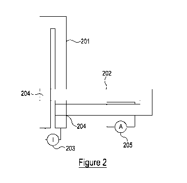
A monitoring device comprising canary tape, allowing the voltage to be
measured
indirectly, is shown in Figure 2. The monitoring device of Figure 2 comprises
a first
conducting element in the form of canary tape 201 for insertion into a
cryogenic system
(e.g. inclusion in the coil structure of a superconducting magnet), and a
second
conducting element in the form of bypass tape 202. Both conducting elements
include
HIS material (in this example in the form of tape), and are arranged to have
minimal
inductance (e.g. doubling back on themselves to minimise the area of the loop
formed).
The HIS material will have no resistance when superconducting, but other parts
of the
canary tape 201 or bypass tape 202 may be resistive (e.g. joints to allow the
tape to
"turn a corner"). The canary tape 201 is connected to a current source 203.
The
bypass tape 202 is connected in parallel with the canary tape via joints 204,
which may
be resistive. There should be at least some resistive (non-superconducting)
material
included in a current path which includes the bypass tape and the joints. This
resistive
material may be present in the joints 204, and/or elsewhere along the bypass
tape 202.
A current detector 205 is provided to detect current in the bypass tape.
CA 03089806 2020-07-28
WO 2019/150091
PCT/GB2019/050241
9
Figure 3 shows an equivalent circuit to the arrangement of Figure 2. The
combined
resistance RB of joints 204 and any resistive non-HTS sections of the bypass
tape 202
is greater than the resistance RT of non-HTS sections (if any) of the canary
tape 201
between the joints. The resistances HTSB and HIST of the HIS sections of the
bypass
tape and canary tape respectively are zero when the current through the HIS is
significantly less than the critical current, i.e. when both tapes are
superconducting. As
such, when current is supplied by the current source 203, the current will
flow in the
canary tape 201 with only a negligible amount flowing in the bypass tape 202,
and so
little or no current will be detected by the current detector 205.
Where the input current I is a significant fraction of the critical current lc
of the canary
tape 201 (e.g. I>0.8 lc), the resistance HIST of HIS material in the canary
tape will
become significant and a voltage will develop across the canary tape.
n
VHTS = LEO(' )
Ic
Where L is the length of the normal section. This voltage will cause a current
to flow
via the joints 204 and bypass tape 202. This current is detected by the
current detector
205. In practice, this will cause a reduction in the current IT through the
canary tape,
and hence a lower voltage, but the principle that a measurable current will
flow through
the bypass tape when I is close to lc holds regardless ¨ the actual current IB
is
relatively complex to calculate, but can be determined as the solution to a
set of
simultaneous equations (e.g. Kirchhoff's current and voltage laws, and the
expression
for VHTs given above), or measured experimentally for calibration purposes.
However,
such accurate calibration is not necessary for basic functioning of the
monitoring device
(e.g. for simple quench detection), as any detected current in the bypass tape
above
background noise indicates that the current in the canary tape is close to the
critical
current.
As a full quench is not required to provide a measurable voltage on the canary
tape,
the monitoring device according to the present disclosure can be considered a
"critical
surface detector" or "critical current detector" rather than only a "quench
detector" - i.e.
the system of the present disclosure monitors the critical current of the
canary tape or
detects changes to the critical current, rather than just detecting quenches.
CA 03089806 2020-07-28
WO 2019/150091
PCT/GB2019/050241
An advantage of the monitoring device described above is that, when the canary
tape
is placed within a superconducting field coil to detect conditions causing a
reduction in
critical current, the bypass tape can be placed in an electromagnetically
quiet location
away from the magnet, so that the current can be measured with less noise.
5
The main example used in this document will be a superconducting magnet and
the
use of canary tape to detect conditions which may result in a quench for such
a
magnet. However, it will be appreciated that the monitoring device disclosed
herein
may be used in a variety of cryogenic or superconducting systems in order to
detect
10 variations in temperature, magnetic field, neutron or ionising radiation
flux, strain, or
other conditions which may vary the critical current of HIS.
A general advantage of the device is that can be used as a distributed sensor.
A very
long canary tape allows the user to monitor a large amount of space. There is
virtually
no limit in size, because there are no ohmic losses or voltage-drops inside a
superconductor in its superconducting state. For example, work is being done
on the
use of superconductors for current transmission over many kilometres. In
theory, it
would be possible to monitor a cable for such a transmission using a single
canary tape
along its entire length, potentially replacing hundreds or even thousands of
individual
localized sensors.
Various techniques may be used to measure the current in the bypass tape, for
example:
= the magnetic field produced by the bypass tape may be measured by a Hall
probe, or the change in magnetic field may be measured by induction in a loop
having a high mutual inductance with the bypass tape;
= a strain gauge may be connected to two parallel sections of the bypass
tape,
and the force between the sections (which will be dependent on the current,
and may be enhanced by providing an additional background field, e.g. using
permanent magnets) can be measured;
= other current measurement techniques as known in the art.
The current measurement may take place in a low-field region away from the
magnet,
and/or within a "magnetic shield" such as a superconducting bulk magnet to
screen out
any background field.
CA 03089806 2020-07-28
WO 2019/150091
PCT/GB2019/050241
11
Various improvements may be made to the canary tape in order to gain more
information about the state of the magnet by monitoring the current in the
bypass tape.
For example, a modulated or AC current may be provided to the canary tape,
with a
peak value which is close to the expected critical current of the canary tape
during
normal operation of the magnet. This may be a pure AC current, or a
combination of
an AC and a DC current (i.e. a modulated current) such that the peak combined
current
is close to the critical current. The use of a pure AC current allows for the
effect of
induced currents in the canary tape to be disregarded (as they will have
opposite
effects on the positive and negative canary tape currents), whereas the use of
a
combination of AC and DC current can allow increased sensitivity of the
detection (as
the current spends more of the cycle close to the critical current of the
tape)A graph
showing an exemplary modulated current waveform is shown in Figure 4A. Figures
4B
to 4D show the current measured in the bypass tape where the critical current
has
values B to D respectively as shown in Figure 4A. In each case, current only
flows in
the bypass tape when the current in the canary tape is above the critical
current. This
example is simplified, in that any current in the bypass tape is noted as "1".
In practice,
there will be an increasing current in the bypass tape as the current in the
canary tape
approaches the critical current, but the transition will be relatively sharp.
As can be
seen, a signal will be measured for a fraction of the critical current period
which
depends on the critical current of the canary tape. As this signal will be
synchronised
with the modulated current supplied, phase sensitive ("synchronous") detection
techniques as known in the art may be used to increase the sensitivity of the
current
measurement, e.g. a lock-in amplifier. While the critical current is between
the
minimum and maximum input current, the lower the critical current in the
canary tape,
the higher the duty cycle of the output will be (i.e. the more time during
each cycle a
current above background noise will be detected).
The use of an AC or modulated input current allows the constant monitoring of
the
critical current of the canary tape. Depending on the changes in critical
current in
single tapes, and the different critical currents of different tapes, various
magnet
properties can be inferred. For example, a drop in critical current for a
single canary
tape or a small group of closely located canary tapes is likely to be due to a
temperature rise. A transient or sudden drop in a more widely spaced group of
canary
CA 03089806 2020-07-28
WO 2019/150091
PCT/GB2019/050241
12
tapes (e.g. all of the tapes on a single return limb) is likely due to strain
in the magnet
or a change in the magnetic field, particularly if the drop in critical
current is related to
the orientation of the canary tape. A gradual reduction of critical current
over time for a
large number of canary tapes could be due to neutron damage to the tapes where
the
tapes are used in a nuclear fusion reactor. Since the canary tapes are located
in close
proximity to the HIS field coils of a magnet, the critical current reductions
of the canary
tapes can be used as a proxy to monitor the "health" or stability of the
magnet, and if
the critical current of the canary tapes falls below a threshold value or the
measured
critical currents show other undesirable properties, then a quench protection
system
can be initiated where power is dumped from the magnet (e.g. to a resistive
load).
Alternatively or additionally, multiple bypass circuits may be attached to a
single canary
tape, with each successive bypass circuit having a higher resistance and
wherein the
total critical current of all bypass tapes except the one with the highest
resistance is
less than the current supplied to the canary tape (and therefore less than the
peak
critical current, i.e. critical current at low temperature and in the absence
of external
magnetic field, of the canary tape). For example, where the current supplied
to the
canary tape is 100A, a bypass circuit B1 may be provided with a critical
current value of
50A and a resistance R1, and a bypass circuit B2 may be provided with a
critical
current value greater than 50A and a resistance R2 which is greater than R1.
When
the canary tape becomes normal, if the resistance of the canary tape is
approximately
equal to R1, then approximately 50A of current will flow in B1 and a small
amount
(depending on the ratio R2/R1) will flow in B2. When the resistance of the
canary tape
is approximately equal to R2, 50A of current will still flow in B1, and a
significant portion
of the remaining 50A of current will flow in B2. When the resistance of the
canary tape
is significantly greater than R2, 50A of current will flow in B1, and
approximately 50A of
current will flow in B2. Therefore, by measurement and calibration of the
currents
flowing in B1 and B2, the resistance of the canary tape (and hence the
severity of any
critical current reduction in the canary tape) can be determined to greater
precision
than with a single bypass tape. Such a sensor is still self-protecting if the
sum of the
critical currents of all bypass tapes is greater than the current supplied to
the canary
tape.
In a similar embodiment, a variable bypass resistance may be provided, for
example by
the use of a potentiometer, by deliberately making sections of the bypass tape
normal
CA 03089806 2020-07-28
WO 2019/150091
PCT/GB2019/050241
13
in a controlled manner, or by heating up a deliberately placed joint in the
bypass
circuit.. By varying the bypass resistance, the resistance of the canary tape
can be
determined, as the dependence of the bypass current on the bypass resistance
will be
determined by the resistance of the canary tape and the (known) input current.
For
example, where the current in the bypass tape is half the input current, the
resistance
of the canary tape is equal to the resistance of the bypass tape.
When installed in a magnet, the canary tape may pass through regions with
different
properties, e.g. higher or lower temperatures or magnetic fields, which will
cause the
critical current to vary along the tape during normal operation of the magnet.
In order
to counteract this effect, and ensure that the tape is uniformly sensitive
along its length,
the width of the superconducting tape in the canary tape may be modulated
along its
length to provide a substantially constant critical current value during
normal operation.
Alternatively or additionally, wider lengths of canary tape may be constructed
by
soldering several narrow tapes together.
With constant width canary tape, or canary tape with modulated width as
described in
the previous paragraph, it is not possible to determine where along the tape a
reduction
of critical current has occurred. This can be achieved by providing multiple
parallel
canary tapes, each having a "measurement width" (i.e. a width providing a
reduced
critical current, which may be modulated as described previously to provide
substantially constant lc) along a part of its length, and a "non-sensitive
width" which is
greater than the measurement width (and so provides a higher lc) on the rest
of its
length. By arranging such tracks so that the "measurement width" sections
overlap
only partially, the location of an lc reduction can be determined ¨ i.e. the
lc reduction
will be detected only on those tapes which have a "measurement width" at the
location
of the lc reduction. One exemplary arrangement is shown in Figure 5, where 6
tapes
5001, 5002, 5003, 5004, 5005, 5006 are provided with "measurement width" 5010
sections, and "non-sensitive width" 5011 sections to form a binary linear
encoder ¨ e.g.
any location (to a resolution equal to the length of the "measurement width"
sections of
the tape 5006) can be specified by a binary number, with the tape 5001
providing the
leftmost bit, the tape 5006 providing the rightmost bit, and the other tapes
arranged
accordingly. For example, a critical current reducing event at each of the
lines 5021
and 5022 would give the corresponding binary outputs 001110 and 101011 (where
"1"
represents a current being detected on the bypass tape connected to that
canary tape).
CA 03089806 2020-07-28
WO 2019/150091
PCT/GB2019/050241
14
In order to reduce the current required by the canary tapes, and thus the
requirement
for high current leads and their associated cooling, the canary tapes may be
configured
to have a relatively low critical current (e.g. by reducing the width of the
tape, or by
deliberate degradation of the tape e.g. through de-oxygenation), so that a
smaller
probe current will still result in sensitive detection. The bypass tape may be
provided
with a higher critical current than the canary tape, which will result in the
canary tape
being "self-protecting", as currents sufficiently high to damage the canary
tape during a
severe reduction in critical current will be redirected entirely into the
bypass tape.
All of the width reductions mentioned above may be achieved by either cutting
through
the HIS layer of the canary tape (e.g. with a laser or scribing tool), or by
heating the
canary tape locally using a laser to the point where the HIS layer of the
canary tape
degrades without cutting the other layers of the tape. Similar techniques may
be used
to provide a "striated canary tape", where the canary tape loop is provided in
a single
tape by cutting an odd number of lines which extend from an end of the tape to
substantially the other end of the tape, with the lines alternating in the end
which they
extend from. Figures 6A and 6B show example tapes with 1 cut and 3 cuts
respectively. The more lines which are cut, the more parallel HIS channels are
provided in the tape, and the more sensitive the canary tape will be. This
allows for a
canary tape to be provided without any resistive sections in the canary tape ¨
meaning
that the ideal case where the resistance of the canary tape between the joints
is zero
can be achieved in practice.
In such a case, it is advantageous for the sensitivity of the canary tape for
the total
resistance RB of the bypass tape and joints to be as close to zero as
possible, while still
being non-zero. However, such a low resistance may, under the influence of an
electric field or changing background field, permit parasitic induced currents
to flow in
the loop created by the bypass tape and canary tape, which will cause noise in
the
measurements. A higher resistance would cause these induced currents to
dissipate
more quickly. In practice, the resistance of the bypass tape may be chosen to
balance
these two factors to achieve an acceptable signal to noise ratio given the
conditions in
which the canary tape is used. The resistance in the bypass loop may be
measured for
calibration purposes by deliberately reducing the critical current of the
canary tape in a
CA 03089806 2020-07-28
WO 2019/150091
PCT/GB2019/050241
non-permanent way (e.g. by heating or the application of a magnetic field)
while
keeping the bypass tape superconducting, and applying a current to the canary
tape.
In order to reduce the effect of induced currents on the critical current
detection, canary
5 tapes and
bypass tapes may be provided in pairs, with each set of canary tape and
bypass tape being connected with an opposite sense, as shown in Figure 7. The
first
canary tape 710 is connected to the first bypass tape 720 such that the upper
leg 721
of the bypass tape connects to the left leg 711 of the canary tape, and the
lower leg
722 of the bypass tape connects to the right leg 712 of the canary tape. The
second
10 canary
tape 730 is connected to the second bypass tape 740 such that the upper leg
741 of the bypass tape connects to the right leg 732 of the canary tape, and
the lower
leg 742 of the bypass tape connects to the left leg 731 of the canary tape.
Both
canary tapes are supplied with current in the same direction (e.g. from the
left leg 711,
731 to the right leg 712, 732). The canary tapes 710, 730 are positioned on
top of
15 each
other, and the bypass tapes 720, 740 are positioned on top of each other. As
such, any currents induced on the loops formed by the canary tapes 710, 730
and
bypass tapes 720, 740 will be induced in opposite directions, and so combining
the
measurements of the currents in the bypass tapes 720, 740 will allow the
induced
currents to be removed.
The canary tape and/or bypass tape need not be made from the same HIS
superconductor as that used in the coils of the magnet, or each other. In
fact, while
the terms "canary tape" and "bypass tape" have been used herein, non-tape HIS
superconductors can be used. For example, the canary tape and/or bypass tape
may
be made from Bi-2212 round multifilamentary wires, whose shape and mechanical
properties may permit them to be more easily embedded in advantageous places
within the magnet. In general, the canary tape is a first conducting element
comprising
HIS material, and the bypass tape is a second conducting element comprising
HIS
material and connected in parallel with the first conducting element.
The monitoring devices may be assembled into a monitoring system, with several
such
devices connected to a single controller which monitors the currents detected
in each
bypass tape to determine when the critical current of the canary tape has been
reduced. The controller may identify the cause of the reduction depending on
the
pattern of critical current reductions, as described above. The controller may
be
CA 03089806 2020-07-28
WO 2019/150091
PCT/GB2019/050241
16
connected to a quench protection system for the magnet, and triggered to dump
energy
from the magnet (via an energy dump system such as a superconducting switch
and
external resistance, or other energy dumps as known in the art) in dependence
upon
the critical current reductions identified. For example, if the critical
current of an
individual canary tape falls below a threshold (either as an absolute value,
or as a
percentage of the expected critical current of the tape), then the energy dump
system
may be triggered.
The monitoring devices in such a monitoring system may be connected in series
to a
single current source, which will result in the same current passing through
each
canary tape. Alternatively, the monitoring devices may be connected in
parallel to a
single current source, with each canary tape being connected via a resistor
having a
resistance much greater (ideally at least an order of magnitude greater, i.e.
at least 10
times greater, or at least 100 times greater) than the resistance values in
the
monitoring device. This will cause the current to divide between the
monitoring devices
on the basis of those resistances. As a further alternative, the monitoring
system may
comprise sets of monitoring devices connected in series, which the sets
themselves
being connected in parallel via a resistor. As a yet further alternative,
separate power
supplies may be provided for the monitoring devices and/or for sets of
monitoring
devices connected in series or in parallel.
The above disclosure can be applied to a variety of HIS magnet systems. In
addition
to the tokamak fusion reactor mentioned above as an example, it may be used
for HIS
magnets in nuclear magnetic resonance imaging (NMR / MRI) devices,
manipulation of
magnetic devices within a non-magnetic medium via magnetic fields (e.g.
robotic
magnetic navigation systems for manipulating medical devices within a
patient), and
magnets for electric motors, e.g. for electronic aircraft. As a further
example, the
disclosure may be applied to proton beam therapy devices comprising HIS magnet
systems which include the disclosed features, where the HIS magnet systems are
used within the accelerator of the PBT device, the quadrupole or dipole
steering
magnets of the PBT device, or any other magnet of the PBT device.