Note: Descriptions are shown in the official language in which they were submitted.
CA 03090431 2020-08-05
WO 2019/161511
PCT/CA2019/050229
RESISTANCE MEASUREMENT ARRAY
CROSS-REFERENCE TO RELATED APPLICATIONS
[0001] This application claims the benefit of priority of U.S.
Provisional Patent
Application No. 62/635,301, filed February 26, 2018 and entitled "RESISTIVE
PRESSURE MEASUREMENT SENSOR ARRAY", which is incorporated herein by
reference in its entirety.
FIELD
[0002] The present disclosure relates to measurement of resistance in
resistive arrays.
BACKGROUND
[0003] Pressure measurement and other sensor arrays are commonly used in
many fields including weight detection in vehicle seats and pressure
distribution
measurements in hospital beds. Devices used in these applications range in
temporal and spatial resolution. Existing technologies may feature high
frequency
scanning, but quickly become expensive with ever-increasing circuit
complexity.
[0004] Ideal designs feature both high spatial density of pressure-sensing
areas (sensors) and a high scanning frequency. High spatial density, high
scanning
frequency sensor arrays may come in the form of a grid of capacitive,
resistive, or
piezoelectric pressure-sensitive areas or sensors, each of which are
intersected by
two electrodes. One of the electrodes is connected to a signal source (the
input
electrode), while the other is connected to an output circuit (the output
electrode).
This formation is repeated for each sensor in an array, and any one electrode
may be
connected to a multitude of sensors, creating a grid of sensors that is each
found at
the intersecting point of an input and an output electrode. By applying a
signal to one
of the input electrodes connected to the source, and reading the signal from
one of
the output electrodes, the electrical characteristics at the individual sensor
isolated at
the intersection of the two electrodes, can be determined. Calibration of the
system
- 1 -
CA 03090431 2020-08-05
WO 2019/161511
PCT/CA2019/050229
allows for these electrical characteristics to be translated into
corresponding pressure
readings, and continual scanning across each of the sensors can be used to
measure the pressure distribution across an entire area over time.
[0005] Application of the signal to only one of the multiple input
electrodes and
election of only one of the multiple output electrodes for reading is
multiplexing, and
allows the isolation of one single sensor within the sensor array. The circuit
scans
through each of the sensors, measuring the pressure at each in a moment before
moving to the next.
[0006] Some previous technologies are directed to increasing spatial
resolution of the sensor array. In some approaches, a comparator amplifier is
implemented at an output electrode with a threshold voltage. Only signals
coming
from the sensor array that are above this predetermined threshold pass through
to
the control circuit and subsequent output. Thus, low pressures (and resulting
low
signals) are ignored. However, in applications where pressure resolution is
the
focus, this process removes relevant data.
[0007] Another focus is on scanning frequency. Discharging
resistances along
every input electrode may discharge trace capacitances in unselected electrode
lines. This method allows for an increase in discharging speed and results in
higher
possible scanning frequencies, but introduces an error in the resistance
reading (and
subsequent interpretation of the applied pressure) at every sensor point, thus
reducing the resolution and precision of the pressure measurement.
[0008] Accommodation of large pressure ranges is another area of
focus in
existing technologies, and is sometimes accomplished by creating a control
circuit
that monitors output readings and adjusts the driving voltage accordingly.
This
approach may increase circuit complexity and manufacturing costs.
SUMMARY
[0009] It is an object of the present disclosure to obviate or
mitigate at least
one disadvantage of previous resistance measurement arrays. Aspects of the
- 2 -
CA 03090431 2020-08-05
WO 2019/161511
PCT/CA2019/050229
present disclosure relate to a system including a circuit and an accompanying
method to measure resistance. The resistance is measured over an array of
nodal
intersection points between input electrodes and output electrodes. The system
and
method facilitate increased resolution on measurement of resistance over an
array.
.. The system and method may be applied to measurement of resistance over an
array
for sensing pressure distribution across a surface.
[0010] The circuit may include an array of variable-resistance areas.
Each
variable-resistance area is defined by a node between an input electrode and
an
output electrode. The circuit includes at least one of the input electrodes,
at least one
of the output electrodes, and at least one additional input or output
electrode,
providing at least two nodes. Each of the input and output electrodes may
intersect a
multitude of variable-resistance areas, defining a multitude of nodes. The
resistance
of the circuit may be sensitive to changes in applied pressure or other
environmental
property at the node. A driving voltage is applied to one of the input
electrodes. The
driving voltage passes through the node, changing the current of the driving
voltage.
An output current is received at one of the number of output electrodes,
isolating an
individual node at the intersection of the two electrodes. The output current
is
converted to an output voltage by a transimpedance amplifier, an integrator
and
control circuit or other current-to-voltage converter circuit. The output
voltage is
.. dependent on the resistance at the isolated node and the driving voltage.
In some
applications of the system and method, the resistance may be dependent on
pressure or another environmental property applied at or to the node,
facilitating
measurement of applied pressure or other environmental properties at the
location of
each node. In some applications of the system and method, an onboard
calibrator
may be used to calibrate the system against known resistance values to account
for
gain of the system. The known resistance values may include an open node with
essentially infinite resistance and a resistor or other electrical component
having a
resistive property, with a known resistance value.
[0011] Where the circuit includes two or more input electrodes, the
driving
voltage is applied to an individual input electrode through an input
multiplexor, which
- 3 -
CA 03090431 2020-08-05
WO 2019/161511
PCT/CA2019/050229
selects only one of the multitude of input electrodes to which to apply the
driving
voltage. Where the circuit includes two or more output electrodes, the output
current
is received at one of the output electrodes by selecting the output electrode
with an
output multiplexor. This way, only one node both receives the signal and is
.. measured, at the intersection of the selected input electrode and the
selected output
electrode. All unselected electrodes are connected directly to a ground
through
single-pole double-throw switches.
[0012] Since individual input electrodes and output electrodes may be
connected to a multitude of nodes, the electrical characteristics such as the
resistance and capacitance of each variable-resistance area in line with the
selected
input electrode and the selected output electrode may affect the output
current and
the output voltage converted from the output current. To mitigate the effects
that
these remaining nodes have on the output current and associated measurement
error, variations in the remaining nodes are isolated from the output voltage
by
connecting the remaining nodes directly to the ground. The output current is
sent to
a single transimpedance amplifier, an integrator and control circuit, or other
current-
to-voltage converter for converting the output current to the output voltage.
The
output voltage can then be converted by an analog-to-digital converter to a
value that
can be visualized or otherwise processed.
[0013] In a first aspect, herein provided is a system and method for
measuring
resistance over an array. The array includes at least three electrodes. Nodes
at
each intersection between input electrodes and output electrodes have variable
resistance. A driving voltage is applied to a selected input electrode and an
output
current is received at a selected output electrode. A selected node is at the
.. intersection of the two selected electrodes and includes an electrical
component with
a resistive property. Remaining electrodes are connected with a ground for
isolating
the selected node from the effects of changes in impedance of the remaining
nodes.
The driving voltage is converted to an output current by resistance at the
selected
node. The output current is converted to an output voltage with a current-to-
voltage
- 4 -
CA 03090431 2020-08-05
WO 2019/161511
PCT/CA2019/050229
converter circuit for measuring the resistance of the electrical component.
The nodes
may be measured as the selected node in sequential or non-sequential patterns.
[0014] In a further aspect, herein provided is a method of measuring
resistance comprising: providing an array of two or more nodes, each of the
nodes
defined at an intersection of an input electrode and an output electrode;
selecting a
selected node at an intersection of a selected input electrode and a selected
output
electrode, the selected node comprising an electrical component having a
resistive
property; grounding remaining input electrodes other than the selected input
electrode; grounding remaining output electrodes other than the selected
output
electrode; applying a driving voltage to the selected input electrode;
converting the
driving voltage to an output current through a resistance of the electrical
component;
receiving the output current at the selected output electrode; and converting
the
output current to an output voltage for measuring the resistance of the
electrical
component.
[0015] In some embodiments, the two or more nodes comprise an open node.
In some embodiments, selecting the selected node is applied sequentially or
non-
sequentially to each of the two or more nodes. In some embodiments, selecting
the
selected node comprises selecting the selected input electrode. In some
embodiments, grounding the remaining input electrodes comprises establishing
electrical communication between the remaining input electrodes and a true
ground,
a positive virtual input ground or a stable fixed voltage. In some
embodiments,
grounding the remaining output electrodes comprises establishing electrical
communication between the remaining output electrodes and a true ground, a
positive virtual input ground or a stable fixed voltage. In some embodiments,
grounding the remaining input electrodes and the remaining output electrodes
comprises establishing electrical communication between the remaining input
electrodes, the remaining output electrodes and a single shared true ground, a
single
shared positive virtual input ground or a single shared stable fixed voltage.
In some
embodiments, converting the output current to an output voltage comprises
application of a transimpedance amplifier to the output current. In some
- 5 -
CA 03090431 2020-08-05
WO 2019/161511
PCT/CA2019/050229
embodiments, converting the output current to an output voltage comprises
application of an integration and control circuit to the output current. In
some
embodiments, the resistance of the electrical component is variable and
dependent
on a first property of an environment around the electrical component, and the
method further comprises determining a value of the first property at the
selected
node with reference to the resistance of the electrical component. In some
embodiments, the first property and the second property are each selected from
pressure, stress, shear, strain, biometrics, temperature, sound intensity or
quality,
light intensity or quality, electromagnetic fields, humidity, moisture,
voltage, current,
.. heart rate or other organ function, atrial fibrillation, breathing or
physical movement.
In some embodiments, the method includes lowering an equivalent resistance of
the
selected node for linearizing the output voltage. In some embodiments, the
method
includes calibrating the array against a pair of calibration nodes comprising
an open
node and a known resistance node to calculate the gain of the array.
[0016] In a further aspect, herein provided is a system for measuring
resistance, the system comprising: at least three electrodes arranged in an
array, the
electrodes comprising at least one input electrode and at least one output
electrode,
and the array comprising at least two nodes, each node being defined at an
intersection between an input electrode and an output electrode; a driving
voltage
source in electrical communication with the input electrode for providing a
driving
voltage to a selected node defined at an intersection between a selected input
electrode and a selected output electrode, the selected node comprising an
electrical
component having a resistive property; a switching system in operative
communication with the electrodes for selecting the selected node; a current-
to-
voltage converter circuit in electrical communication with the output
electrode for
receiving an output current from the selected node and converting the output
current
to an output voltage; and a ground in communication with the array for
grounding
remaining input electrodes other than the selected input electrode, and for
grounding
remaining output electrodes other than the selected output electrode, for
isolating the
selected node from electrical effects on the array other than at the selected
node.
- 6 -
CA 03090431 2020-08-05
WO 2019/161511
PCT/CA2019/050229
[0017] In some embodiments, the electrodes comprise at least two
input
electrodes; the switching system is in operative communication with the at
least two
input electrodes; and the system further comprises an input multiplexor in
communication with the input electrodes for establishing electrical
communication
between the selected input electrode and the driving signal source, and
between the
remaining input electrodes and the ground. In some embodiments, the at least
three
electrodes comprise at least two output electrodes; the switching system is in
operative communication with the at least two output electrodes; and the
system
further comprises an output multiplexor in communication with the output
electrodes
for establishing electrical communication between the selected output
electrode and
the current-to-voltage converter circuit, and between the remaining output
electrodes
and the ground. In some embodiments, the switching system comprises a single-
pole double-throw switch. In some embodiments, the at least two nodes comprise
at
least three nodes, and the nodes are arranged orthogonally or non-orthogonally
with
respect to one another. In some embodiments, a resistance at the selected node
is
variable and dependent on a first property of an environment around the array.
In
some embodiments, the resistance at the selected node is variable and
dependent
on a second property of the environment. In some embodiments, the first
property
and the second property are each selected from the properties consisting of
pressure, stress, shear, strain, biometrics, temperature, sound intensity or
quality,
light intensity or quality, electromagnetic fields, humidity, moisture,
voltage, current,
heart rate or other organ function, atrial fibrillation, breathing or physical
movement.
In some embodiments, the system includes an analog-to-digital converter in
electronic communication with the current-to-voltage converter circuit for
receiving
the output voltage and converting the output voltage to a digital signal; and
a
processor in electronic communication with the analog-to-digital converter and
configured for receiving the digital signal, processing the digital signal;
and
communicating the property or the second property to a user of the system. In
some
embodiments, the at least two nodes comprise an open node. In some
embodiments, the driving voltage source comprises a DC voltage source. In some
- 7 -
CA 03090431 2020-08-05
WO 2019/161511
PCT/CA2019/050229
embodiments, the current-to-voltage converter circuit comprises a
transimpedance
amplifier. In some embodiments, the current-to-voltage converter circuit
comprises
an integrator and control circuit. In some embodiments, the ground comprises a
true
ground, a virtual ground or a stable fixed voltage. In some embodiments, the
system
includes an analog-to-digital converter in electronic communication with the
current-
to-voltage converter circuit for receiving the output voltage and converting
the output
voltage to a digital signal. In some embodiments, the system includes a
processor in
electronic communication with the analog-to-digital converter for receiving
the digital
signal and processing the digital signal. In some embodiments, the system
includes
a linearization circuit in electrical communication with the electrodes for
lowering the
equivalent resistance of the selected node for linearizing the output voltage.
In some
embodiments, the system includes a calibrator in electrical communication with
the
electrodes for calibrating the array against a pair of calibration nodes
comprising an
open node and a known resistance node.
[0018] In a further aspect, herein provided is a method of measuring
resistance comprising: providing an array of two or more nodes, each of the
nodes
defined at an intersection of an input electrode and an output electrode;
selecting a
selected node at an intersection of a selected input electrode and a selected
output
electrode, the selected node comprising an electrical component having a
resistive
property; grounding remaining input electrodes other than the selected input
electrode; grounding remaining output electrodes other than the selected
output
electrode; applying a driving voltage to the selected input electrode;
converting the
driving voltage to an output current through a resistance of the electrical
component;
receiving the output current at the selected output electrode; and converting
the
output current to an output voltage with an integration and control circuit
for
measuring the resistance of the electrical component.
[0019] In some embodiments, the two or more nodes comprise an open
node.
In some embodiments, selecting the selected node is applied sequentially or
non-
sequentially to each of the two or more nodes. In some embodiments, selecting
the
selected node comprises selecting the selected input electrode. In some
- 8 -
CA 03090431 2020-08-05
WO 2019/161511
PCT/CA2019/050229
embodiments, grounding the remaining input electrodes comprises establishing
electrical communication between the remaining input electrodes and a true
ground,
a positive virtual input ground or a stable fixed voltage. In some
embodiments,
grounding the remaining output electrodes comprises establishing electrical
communication between the remaining output electrodes and a true ground, a
positive virtual input ground or a stable fixed voltage. In some embodiments,
grounding the remaining input electrodes and the remaining output electrodes
comprises establishing electrical communication between the remaining input
electrodes, the remaining output electrodes and a single shared true ground, a
single
.. shared positive virtual input ground or a single shared stable fixed
voltage. In some
embodiments, converting the output current to an output voltage comprises
application of a transimpedance amplifier to the output current. In some
embodiments, the resistance of the electrical component is variable and
dependent
on a first property of an environment around the electrical component, and the
method further comprises determining a value of the first property at the
selected
node with reference to the resistance of the electrical component. In some
embodiments, the first property and the second property are each selected from
pressure, stress, shear, strain, biometrics, temperature, sound intensity or
quality,
light intensity or quality, electromagnetic fields, humidity, moisture,
voltage, current,
heart rate or other organ function, atrial fibrillation, breathing or physical
movement.
In some embodiments, the method includes lowering an equivalent resistance of
the
selected node for linearizing the output voltage. In some embodiments, the
method
includes calibrating the array against a pair of calibration nodes comprising
an open
node and a known resistance node to calculate the gain of the array.
[0020] In a further aspect, herein provided is a system for measuring
resistance, the system comprising: at least three electrodes arranged in an
array, the
electrodes comprising at least one input electrode and at least one output
electrode,
and the array comprising at least two nodes, each node being defined at an
intersection between an input electrode and an output electrode; a driving
voltage
source in electrical communication with the input electrode for providing a
driving
- 9 -
CA 03090431 2020-08-05
WO 2019/161511
PCT/CA2019/050229
voltage to a selected node defined at an intersection between a selected input
electrode and a selected output electrode, the selected node comprising an
electrical
component having a resistive property; a switching system in operative
communication with the electrodes for selecting the selected node; an
integrator and
.. control circuit in electrical communication with the output electrode for
receiving an
output current from the selected node and converting the output current to an
output
voltage; and a ground in communication with the array for grounding remaining
input
electrodes other than the selected input electrode, and for grounding
remaining
output electrodes other than the selected output electrode, for isolating the
selected
node from electrical effects on the array other than at the selected node.
[0021] In some embodiments, the electrodes comprise at least two
input
electrodes; the switching system is in operative communication with the at
least two
input electrodes; and the system further comprises an input multiplexor in
communication with the input electrodes for establishing electrical
communication
between the selected input electrode and the driving signal source, and
between the
remaining input electrodes and the ground. In some embodiments, the at least
three
electrodes comprise at least two output electrodes; the switching system is in
operative communication with the at least two output electrodes; and the
system
further comprises an output multiplexor in communication with the output
electrodes
for establishing electrical communication between the selected output
electrode and
the current-to-voltage converter circuit, and between the remaining output
electrodes
and the ground. In some embodiments, the switching system comprises a single-
pole double-throw switch. In some embodiments, the at least two nodes comprise
at
least three nodes, and the nodes are arranged orthogonally or non-orthogonally
with
respect to one another. In some embodiments, a resistance at the selected node
is
variable and dependent on a first property of an environment around the array.
In
some embodiments, the resistance at the selected node is variable and
dependent
on a second property of the environment. In some embodiments, the first
property
and the second property are each selected from the properties consisting of
pressure, stress, shear, strain, biometrics, temperature, sound intensity or
quality,
-10-
CA 03090431 2020-08-05
WO 2019/161511
PCT/CA2019/050229
light intensity or quality, electromagnetic fields, humidity, moisture,
voltage, current,
heart rate or other organ function, atrial fibrillation, breathing or physical
movement.
In some embodiments, the system includes an analog-to-digital converter in
electronic communication with the current-to-voltage converter circuit for
receiving
the output voltage and converting the output voltage to a digital signal; and
a
processor in electronic communication with the analog-to-digital converter and
configured for receiving the digital signal, processing the digital signal;
and
communicating the property or the second property to a user of the system. In
some
embodiments, the at least two nodes comprise an open node. In some
.. embodiments, the driving voltage source comprises a DC voltage source. In
some
embodiments, the current-to-voltage converter circuit comprises a
transimpedance
amplifier. In some embodiments, the ground comprises a true ground, a virtual
ground or a stable fixed voltage. In some embodiments, the system includes an
analog-to-digital converter in electronic communication with the current-to-
voltage
converter circuit for receiving the output voltage and converting the output
voltage to
a digital signal. In some embodiments, the system includes a processor in
electronic
communication with the analog-to-digital converter for receiving the digital
signal and
processing the digital signal. In some embodiments, the system includes a
linearization circuit in electrical communication with the electrodes for
lowering the
.. equivalent resistance of the selected node for linearizing the output
voltage. In some
embodiments, the system includes a calibrator in electrical communication with
the
electrodes for calibrating the array against a pair of calibration nodes
comprising an
open node and a known resistance node.
[0022] In a further aspect, herein provided is a method of measuring
resistance comprising: providing an array of two or more nodes, each of the
nodes
defined at an intersection of an input electrode and an output electrode;
calibrating
the array against a pair of calibration nodes comprising an open node and a
known
resistance node to calculate the gain of the array; selecting a selected node
at an
intersection of a selected input electrode and a selected output electrode,
the
selected node comprising an electrical component having a resistive property;
- 11 -
CA 03090431 2020-08-05
WO 2019/161511
PCT/CA2019/050229
grounding remaining input electrodes other than the selected input electrode;
grounding remaining output electrodes other than the selected output
electrode;
applying a driving voltage to the selected input electrode; converting the
driving
voltage to an output current through a resistance of the electrical component;
receiving the output current at the selected output electrode; and converting
the
output current to an output voltage with a current-to-voltage converter
circuit for
measuring the resistance of the electrical component.
[0023] In some embodiments, the two or more nodes comprise an open
node.
In some embodiments, selecting the selected node is applied sequentially or
non-
sequentially to each of the two or more nodes. In some embodiments, selecting
the
selected node comprises selecting the selected input electrode. In some
embodiments, grounding the remaining input electrodes comprises establishing
electrical communication between the remaining input electrodes and a true
ground,
a positive virtual input ground or a stable fixed voltage. In some
embodiments,
grounding the remaining output electrodes comprises establishing electrical
communication between the remaining output electrodes and a true ground, a
positive virtual input ground or a stable fixed voltage. In some embodiments,
grounding the remaining input electrodes and the remaining output electrodes
comprises establishing electrical communication between the remaining input
electrodes, the remaining output electrodes and a single shared true ground, a
single
shared positive virtual input ground or a single shared stable fixed voltage.
In some
embodiments, converting the output current to an output voltage comprises
application of a transimpedance amplifier to the output current. In some
embodiments, converting the output current to an output voltage comprises
application of an integration and control circuit to the output current. In
some
embodiments, the resistance of the electrical component is variable and
dependent
on a first property of an environment around the electrical component, and the
method further comprises determining a value of the first property at the
selected
node with reference to the resistance of the electrical component. In some
embodiments, the first property and the second property are each selected from
- 12 -
CA 03090431 2020-08-05
WO 2019/161511
PCT/CA2019/050229
pressure, stress, shear, strain, biometrics, temperature, sound intensity or
quality,
light intensity or quality, electromagnetic fields, humidity, moisture,
voltage, current,
heart rate or other organ function, atrial fibrillation, breathing or physical
movement.
[0024] In a further aspect, herein provided is a system for measuring
resistance, the system comprising: at least three electrodes arranged in an
array, the
electrodes comprising at least one input electrode and at least one output
electrode,
and the array comprising at least two nodes, each node being defined at an
intersection between an input electrode and an output electrode; a calibrator
in
electrical communication with the electrodes for calibrating the array against
a pair of
calibration nodes comprising an open node and a known resistance node; a
driving
voltage source in electrical communication with the input electrode for
providing a
driving voltage to a selected node defined at an intersection between a
selected input
electrode and a selected output electrode, the selected node comprising an
electrical
component having a resistive property; a switching system in operative
communication with the electrodes for selecting the selected node; a current-
to-
voltage converter circuit in electrical communication with the output
electrode for
receiving an output current from the selected node and converting the output
current
to an output voltage; and a ground in communication with the array for
grounding
remaining input electrodes other than the selected input electrode, and for
grounding
remaining output electrodes other than the selected output electrode, for
isolating the
selected node from electrical effects on the array other than at the selected
node.
[0025] In some embodiments, the electrodes comprise at least two
input
electrodes; the switching system is in operative communication with the at
least two
input electrodes; and the system further comprises an input multiplexor in
.. communication with the input electrodes for establishing electrical
communication
between the selected input electrode and the driving signal source, and
between the
remaining input electrodes and the ground. In some embodiments, the at least
three
electrodes comprise at least two output electrodes; the switching system is in
operative communication with the at least two output electrodes; and the
system
further comprises an output multiplexor in communication with the output
electrodes
-13-
CA 03090431 2020-08-05
WO 2019/161511
PCT/CA2019/050229
for establishing electrical communication between the selected output
electrode and
the current-to-voltage converter circuit, and between the remaining output
electrodes
and the ground. In some embodiments, the switching system comprises a single-
pole double-throw switch. In some embodiments, the at least two nodes comprise
at
least three nodes, and the nodes are arranged orthogonally or non-orthogonally
with
respect to one another. In some embodiments, a resistance at the selected node
is
variable and dependent on a first property of an environment around the array.
In
some embodiments, the resistance at the selected node is variable and
dependent
on a second property of the environment. In some embodiments, the first
property
and the second property are each selected from the properties consisting of
pressure, stress, shear, strain, biometrics, temperature, sound intensity or
quality,
light intensity or quality, electromagnetic fields, humidity, moisture,
voltage, current,
heart rate or other organ function, atrial fibrillation, breathing or physical
movement.
In some embodiments, the system includes an analog-to-digital converter in
electronic communication with the current-to-voltage converter circuit for
receiving
the output voltage and converting the output voltage to a digital signal; and
a
processor in electronic communication with the analog-to-digital converter and
configured for receiving the digital signal, processing the digital signal;
and
communicating the property or the second property to a user of the system. In
some
embodiments, the at least two nodes comprise an open node. In some
embodiments, the driving voltage source comprises a DC voltage source. In some
embodiments, the current-to-voltage converter circuit comprises a
transimpedance
amplifier. In some embodiments, the current-to-voltage converter circuit
comprises
an integrator and control circuit. In some embodiments, the ground comprises a
true
ground, a virtual ground or a stable fixed voltage. In some embodiments, the
system
includes an analog-to-digital converter in electronic communication with the
current-
to-voltage converter circuit for receiving the output voltage and converting
the output
voltage to a digital signal. In some embodiments, the system includes a
processor in
electronic communication with the analog-to-digital converter for receiving
the digital
signal and processing the digital signal. In some embodiments, the system
includes
- 14 -
CA 03090431 2020-08-05
WO 2019/161511
PCT/CA2019/050229
a linearization circuit in electrical communication with the electrodes for
lowering the
equivalent resistance of the selected node for linearizing the output voltage.
[0026] Other aspects and features of the present disclosure will
become
apparent to those ordinarily skilled in the art upon review of the following
description
of specific embodiments in conjunction with the accompanying figures.
BRIEF DESCRIPTION OF THE DRAWINGS
[0027] Embodiments of the present disclosure will now be described,
by way
of example only, with reference to the attached figures, in which reference
numerals
sharing a common final two digits refer to corresponding features across
figures (e.g.
the selected node 102a, selected node 302a, selected node 402a, selected node
502a, selected node 602a, etc.).
[0028] Fig. 1 is a circuit drawing of a resistance measurement array;
[0029] Fig. 2 is a schematic representation of an equivalent circuit on a
selected node in the resistance measurement array of Fig. 1;
[0030] Fig. 3 is a circuit drawing of a resistance measurement array;
[0031] Fig. 4 is a circuit drawing of a resistive pressure sensor
array;
[0032] Fig. 5 is a circuit drawing of a resistance measurement array;
and
[0033] Fig. 6 is a circuit drawing of a resistance measurement array.
DETAILED DESCRIPTION
[0034] Generally, the present disclosure provides a method and system
for
measuring resistance at a selected node of a resistance measurement array.
[0035] A system and method for measuring resistance in a resistance
measurement array. At least one input electrode and at least one output
electrode,
totaling at least three electrodes, define a resistive sensor array. Each
intersection
between an input electrode and an output electrode defines a node. Each node
has
an electrical component having a resistive property. A signal source for
generating a
driving voltage is in electrical communication with the input electrodes.
Input
-15-
CA 03090431 2020-08-05
WO 2019/161511
PCT/CA2019/050229
switches allow selective application of the driving voltage to a selected
input
electrode. Output switches allow selective detection of an output voltage at a
selected output electrode. Together the input switches and the output switches
provide a switching system in operative communication with the input
electrodes and
the output electrodes for selecting the selected node. The output voltage is
converted from an output current, which results from passing the driving
voltage
through the resistance of the selected node. A transimpedance amplifier,
integrator
and control circuit or other current-to-voltage converter circuit converts the
output
current to the output voltage and amplify the output voltage downstream of the
output
electrode.
[0036] Grounds or other reference voltage sources are applied to
remaining
input electrodes other than the selected input electrode, and to remaining
output
electrodes other than the selected output electrode, for isolating a selected
node
from the effects of changes in impedance of nodes other than the selected
node.
The selected node is at the intersection of the selected input electrode and
the
selected output electrode. The selected node may be changed by changing the
selected input electrode or changing selected output electrode. The output
voltage
measured as a result of the resistance at the selected node may be
communicated to
a processor. The processor may calculate a pressure or other environmental
property at the selected node based on a variable resistance, which is
sensitive to
the environmental property, at the selected node.
[0037] A node may have no resistance, infinite resistance (i.e. an
open node),
finite resistance, or may have an electrical component whose reading can be
converted to resistance. The electrical component may include a sensor that
converts
a physical condition or other environmental property at the node into a
resistance
such as biometric sensors, stress sensors, shear sensors, strain sensors,
pressure
sensors, thermistors, microphone, acoustic sensors, light intensity sensors,
magnetic
sensors, humidity sensors, voltage sensors, current sensors, heart rate
sensors,
breathing rate sensors, atrial fibrillation sensors, activity sensors (step,
calorie,
activity recognition, sleep quality, walking, running, sitting, standing, slip
and fall
- 16 -
CA 03090431 2020-08-05
WO 2019/161511
PCT/CA2019/050229
detection, fatigue detection, ovulation, and blood pressure). Arrays may be
homogeneous or heterogeneous arrays of electrical components, and may include
sensors for a variety of properties of the environment. More than one type of
electrical component or sensor may be located at the nodes of the same array.
More
than one electrical component or sensor may be located at each node. Groupings
of
sensors or other electrical components or may occur in regions of a resistive
array.
[0038] The input electrodes and the output electrodes may be arranged
into
any suitable pattern to provide the measurement array. Orthogonal relative
orientations between the input and output electrodes in rectilinear or other
arrangements, or non-orthogonal relative orientations may be used on any given
application of the system. Using an example where the input electrodes are in
columns and the output electrodes in rows, the driving voltage source may be
applied
to one column of input electrodes and the unselected columns are grounded to
an
input ground through use of input switches. One row of output electrodes is
correspondingly selected and connected to a transimpedance amplifier,
integrator
circuit or other current-to-voltage converting electronic circuit, and the
unselected
output electrode rows are grounded using output switches. The selected input
electrode and the selected output electrode intersect at a selected node.
Output
current results from application of the driving voltage to the selected node.
The
output current is converted to an output voltage by the transimpedance
amplifier,
integrator circuit or other current-to-voltage converting electronic circuit.
The output
voltage is passed to an analog to digital converter or other measuring device.
The
grounding of the unselected rows and columns isolates the selected node at
which
resistance is being measured from the effects of the impedance of the nodes
other
than the selected node.
[0039] The input switches and the output switches may include single-
pole
double-throw switches, which may include low on-resistance single-pole double
¨
throw switches. The single-pole double-throw switches are connected with
grounds
to mitigate errors regardless of scanning speed. The switches may introduce
some
internal capacitance to the system, which in high-speed scanning systems may
-17-
CA 03090431 2020-08-05
WO 2019/161511
PCT/CA2019/050229
increase the discharge time constant of the sensors defined by each node, and
potentially reducing scanning speed. For applications where scanning speed is
not
relevant, one of the single-pole double-throw switches may be directly
connected to
ground, mitigating errors that may result when resistors discharge into a
ground.
[0040] A transimpedance amplifier directly converts the output current to
output voltage.
[0041] An integrator and control circuit may also be used to convert
the output
current to output voltage, and acts on integrated current, which may decrease
the
noise in the circuit. Two analog switches and additional circuitry to control
the
switches may be included to support use of the integrator. An integrator
circuit may
include an opamp, a reset switch and an integrating capacitor.
[0042] The output voltage is not fed into a feedback control circuit
that allows
for the adjustment of the driving voltage. Rather, the same driving voltage
source is
in electrical communication with each node, which may provide efficiencies,
reduce
complexity and reduce circuit cost compared with systems that include a
feedback
control circuit.
[0043] The system may be applied to clothing, vests, belts, foot
pressure
insoles, shoes, orthotics, socks, body suits, smart bandages, EEG caps, foam,
sleep
surfaces and other furniture, blankets, car seats, robotic surgery with haptic
feedback, augmentation of sensation, direction finding, gunshot detection and
resistive touch screens. In addition to providing design information, the
system can
be used for other applications. For example, the system can be used to monitor
apnea or to detect the exit of a patient from a bed. In the case of a
resistance
measurement array for measuring pressure, the weight of a patient can be
determined and indicated on a display by summing the pressures that are
measured
at each node. The pressures that are measured at each node may be converted to
colours and displayed on a display. The resistive array may be used as part of
a
dynamic feedback system in which the contour of a bed is automatically
adjusted in
response to movements of the patient to accommodate various reclining
positions.
-18-
CA 03090431 2020-08-05
WO 2019/161511
PCT/CA2019/050229
[0044] The resistance measurement array may use variable resolution
scanning. With variable resolution scanning, the input multiplexor may be
powered
up and taken out of reset. The voltage representing the selected node
resistance is
present on the multiplexers' analog output for analog to digital conversion.
To read
the next sensor, a clock pulse is provided from a processor to a counter. The
analog
value representing the resistance of the next node appears on the output
electrode
and settles, then is ready for analog to digital conversion. In applications
of the
system in which the nodes are scanned in a sequence, scanning resolution may
be
selected by skipping some of the nodes in a scan pattern. For example, a
protocol
could include resetting the system, reading a first node, clocking the counter
three
times, reading a fourth node, clocking the counter three times, reading a
seventh
node and continuing. Once resistance has been measured at the final node, then
1/4
of the resistance measurement array will have been read, reading from 1/4 of
the area
resolution of the sensors.
[0045] The system may also be applied to non-sequential scanning of the
resistance measurement array. The multiplexer and clocking to a selected node
precedes the current-to-voltage conversion of the output current and analog-to-
digital
conversion of the resulting output voltage. This may be repeated to collect
output
voltages for other selected nodes in a selected sequence. Alternatively, if
the input
multiplexor is driven by a loadable counter instead of a sequential counter,
then a
scanning pattern for the selected nodes may be loaded into the counter and the
resistance of the selected node read based on the scanning pattern.
[0046] A calibration circuit may be used to calibrate the system. The
calibration circuit may provide a known value, such as resistance, between the
selected input electrode and the selected output electrode. Upon start-up of
the
pressure measurement system, the calibration circuit may be applied to an open
node (i.e. infinite resistance) and a known resistor, and compute the gain of
the
system.
[0047] Fig. 1 is a resistance measurement system 100 in operation.
The
system 100 includes a driving voltage source 110 in electrical communication
with an
-19-
CA 03090431 2020-08-05
WO 2019/161511
PCT/CA2019/050229
input circuit 120. The input circuit 120 is also in electrical communication
with an
output circuit 130. A measurement array 104 is positioned intermediate the
input
circuit 120 and the output circuit 130. A transimpedance amplifier 140 is in
communication with the output circuit 130 for receiving an output current, and
converting and amplifying the output current to an output voltage. The
transimpedance amplifier 140 is in communication with a processor 180 for
receiving
and processing the output voltage.
[0048] The driving voltage source 110 provides a driving voltage to
the input
circuit 120, causing current to flow into the selected input electrode 106a
(described
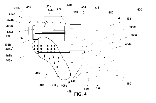
below). The input switches 124 (described below) route error currents to the
input
ground 126 (described below) away from the selected node 102a (described
below).
Similarly, the output switches 134 (described below) route error currents to
the
ground 136 (described below) and away from the transimpedance amplifier 140.
The
driving voltage source 110 is connected a driving voltage ground 116.
Isolating the
error currents from the selected input electrode 106a facilitates measurement
of
resistance at the selected node 102a. Where the system 100 is applied to
sensing or
detection of a property external to the system 100 based on changes in the
resistance of the measurement array 104 resulting from changes in the
property, the
improved sensitivity of the sensor may be facilitated by isolation of the
error.
[0049] The input circuit 120 is in communication with the measurement array
104 through a plurality of input electrodes 106. The output circuit 130 is in
communication with the measurement array 104 through a plurality of output
electrodes 108. A plurality of nodes 102 are defined at intersections between
the
input electrodes 106 and the output electrodes 108. The plurality of nodes 102
are
distributed in the measurement array 104.
[0050] The measurement array 104 includes the nodes 102 at
intersections of
the plurality of the input electrodes 106 and plurality of the output
electrodes 108.
The input electrodes 106 and the output electrodes 108 are organized into
columns
and orthogonal rows. The relative orientations of the rows and columns may be
interchangeable, or the input electrodes 106 and the output electrodes 108
applied in
- 20 -
CA 03090431 2020-08-05
WO 2019/161511
PCT/CA2019/050229
non-orthogonal orientations between leads of input electrodes and leads of
output
electrodes in a resistance measurement system. The columns in the measurement
array 104 include the input electrodes 106, and the rows include the output
electrodes 108. The measurement array 104 may be applied for detecting changes
.. in a property of an environment or other system being measured.
[0051] At each intersection of the input electrodes 106 and the
output
electrodes 108 is one of the nodes 102. Each node 102 may have a resistance
that
is sensitive to, and altered by, changes in a property of the environment
external to
the system 100 (e.g. pressure, stress, strain, biometrics, temperature, sound
intensity
.. or quality, light intensity or quality, electromagnetic fields, humidity,
moisture, voltage,
current, heart rate or other organ function, atrial fibrillation, breathing,
physical
movement, etc.). Variations in the property at a node 102 may result in
measurable
variations in the resistance the of measurement array 104 at the node 102
between
the input electrode 106 and the output electrode 108. The magnitude of the
property
applied to each node 102 correlates to a measurable and predictable change in
the
resistance of the measurement array 104 at the node 102.
[0052] The input circuit 120 allows isolation of one input electrode
106 to
receive the driving voltage from the driving voltage source 110 and apply the
driving
voltage to the measurement array 104. The input circuit 120 includes an input
multiplexor 122 and a plurality of input switches 124. The input switches 124
may be
single-pole double-throw switches. The input switches 124 may be connected to
an
input ground 126. The input ground 126 may provide a true ground, a positive
virtual
input ground, a stable fixed voltage or any suitable ground.
[0053] Each of the input electrodes 106 is connected with an input
switch 124.
The input multiplexor 122 is also connected to each of the input switches 124.
Each
input electrode 106 may be connected to either the driving voltage source 110
or the
input ground 126 through the input switches 124 by selection from the input
multiplexor 122.
[0054] The output circuit 130 includes an output multiplexor 132 and
output
switches 134. The output switches 134 may be single-pole double-throw output
- 21 -
CA 03090431 2020-08-05
WO 2019/161511
PCT/CA2019/050229
switches. The output switches 134 are connected to an output ground 136. The
output ground 136 may include a true ground, a positive virtual input ground,
a stable
fixed voltage or any suitable ground. The driving voltage ground 116, the
input
ground 126 and the output ground 136 are electrically equivalent regardless of
the
specific ground applied at each of driving voltage ground 116, the input
ground 126
and the output ground 136. The driving voltage ground 116, the input ground
126
and the output ground 136 may be in electrical communication.
[0055] Together, the input switches 124 and the output switches 134
provide a
switching system in operative communication with the input electrodes 106 and
the
output electrodes 108 for selecting the selected node 102a (described below).
[0056] The input multiplexor 122 and the input switches 124 are
controlled by
a counter 128. The counter 128 opens and closes the input switches 124 and the
output switches 134 to select different nodes 102 from which to acquire data
of the
property being sensed by the system 100 or for other applications of measuring
resistance. The output multiplexor 132 is in communication with the counter
128.
The counter 128 may be configured to scan through the input electrodes 106 and
then increment the output multiplexor 132 to scan the next output electrode
108 as
the selected output electrode 108a. The scan rate of the input multiplexor 120
may
be n times the scan rate of output multiplexor 132 where n is the number of
input
switches 124. The scan rate of the output multiplexor 132 may ben times the
scan
rate of multiplexor 122 where n is the number of output switches 134.
[0057] The transimpedance amplifier 140 is configured to transform
the output
current into an amplified, measurable voltage. The system 100 uses the driving
voltage to create a current at the selected node 102a and the transimpedance
.. amplifier 140 converts the current to voltage. The transimpedance amplifier
140 may
be substituted by any operational amplifier configured as a transimpedance
amplifier.
The transimpedance amplifier may be substituted with an integrator and control
circuit, as in the system 300 of Fig 3, the system 400 of Fig 4, the system
500 of Fig
5 and the system 600 of Fig 6. A transimpedance amplifier directly converts
the
output current to output voltage. An integrator also converts the output
current to
- 22 -
CA 03090431 2020-08-05
WO 2019/161511
PCT/CA2019/050229
output voltage, with the current being integrated. An integrator circuit may
decrease
the noise in the amplified output voltage. When applying an integrator
circuit, two
analog switches may be included in the system along with additional circuitry
to
control the switches. An integrator circuit may include an opamp, a reset
switch and
an integrating capacitor.
[0058] The transimpedance amplifier 140 is connected to an amplifier
ground
146. The amplifier ground 146 may be a true ground, a positive virtual input
ground,
a stable fixed voltage, or any suitable ground.
[0059] A linearization circuit 138 is located between the input
circuit 120 and
the output circuit 130 and in parallel with the measurement array 104. The
linearization circuit 138 is configured to increase the output voltage into a
range with
resolution selected for a particular application of the system 100. The
linearization
circuit 138 may include a large value resistor. The large value resistor may
be
applied in the linearization circuit 138 to lower the equivalent resistance of
the
selected node 102a when applying the driving voltage to a selected node 102a
with a
high resistance, linearizing the output voltage across various ranges of the
resistance
of the electrical component of the selected node 102a. The linearization
circuit 138
reduces the resistance of the circuit including the input circuit 120, the
measurement
array 104 and the output circuit 130, increasing the output voltage. The
linearizing
circuit facilitates measurement of larger resistance values at the selected
node 102a,
and correspondingly lower output currents and output voltages, than the
circuit
including the input circuit 120, the measurement array 104 and the output
circuit 130
would otherwise be able to measure.
[0060] In operation, resistance at a selected node 102a may be
measured
when the driving voltage is applied to a selected input electrode 106a, and
the output
current is received at a selected output electrode 108a. The magnitude of the
output
current is converted to voltage through the transimpedance amplifier 140 and
the
magnitude of the output voltage will depend on the resistance at the selected
node
102a. The resistance at the selected node 102a changes with the magnitude of
the
property applied at the selected node 102a. The driving voltage is applied to
the
- 23 -
CA 03090431 2020-08-05
WO 2019/161511
PCT/CA2019/050229
selected input electrode 106a and not applied to remaining input electrodes
106b.
The resistance at the selected node 102a is calculated from the measured
voltage
from the following equations:
[0061] !measure = (Vv-Vd)/R (1)
[0062] Vo = Vv + !measure X Rg
(2)
[0063] R = ((Vv ¨ Vd) X Rg) / (Vo- Vv) (3)
[0064] In equations 1, 2 and 3, R is the resistor being measured, Vv
is the
voltage of virtual ground (e.g. 0.2 V), Vd is the driving voltage (e.g.
0.15V), !measure is
the current flowing through R, Rg is the value of gain resistor on
transimpedance
amplifier, and Vo is the Voltage output from the transimpedance amplifier
while
!measure flows through R.
[0065] When the input multiplexor 122 selects the selected input
electrode
106a to receive the driving voltage from the driving voltage source 110, the
selected
input electrode 106a is connected to the driving voltage source 110 through
the
selected input switch 124a and remaining input electrodes 106b are each
connected
with the input ground 126 through remaining input switches 124b. The selected
input
switch 124a provides electrical communication between the driving voltage
source
110 and the selected input electrode 106a only, and not with the remaining
input
electrodes 106b.
[0066] The counter 128 counts incrementally, and selects a new input
electrode 106 to be the selected input electrode 106a with the driving voltage
source
110 as the count increments. In this way, the counter 128 and the input
circuit 120
scan across the input electrodes 106, placing the driving voltage source 110
in
electrical communication with each input electrode 106 sequentially. The
counter
128 also selects an output electrode 108 to be included in an output circuit
130 as
the selected output electrode 108a.
[0067] The output multiplexor 132 selects the selected output
electrode 108a
from which to receive the output current. A selected output switch 134a is
associated
with the selected output electrode 108a, providing electrical communication
with the
- 24 -
CA 03090431 2020-08-05
WO 2019/161511
PCT/CA2019/050229
transimpedance amplifier 140. The remaining output electrodes 108b are each
connected to the output ground 136 through remaining output switches 134b.
[0068] The selected input electrode 106a and the selected output
electrode
108a define the selected node 102a at the intersection of the selected input
electrode
106a and the selected output electrode 108a. The selected node 102a receives
the
driving voltage from the driving voltage source 110. The resistance of the
measurement array 104 at the selected node 102a determines the output current
that
results from the driving voltage. The output voltage is converted from the
output
current and amplified by the transimpedance amplifier 140 for provision to the
processor 180. The remaining output electrodes 108b are connected to the
output
ground 136 through the remaining output switches 134b, isolating the selected
node
102a from the effects of impedance, resistance or other electrical changes in
the
remaining nodes 102b.
[0069] A calibration circuit 150 may be used to calibrate the system
100. The
calibration circuit 150 may effectively act as a known value, such as
resistance,
between the selected input electrode 106a and the selected output electrode
108a.
Upon start-up of the system 100, the processor 180 or a processor on another
system (not shown) may read the calibration circuit 150 initially, and compute
the
gain of the system 100.
[0070] Calibration of the system 100 may include measurement of Vv for an
open node (i.e. infinite resistance) and ((Vv-Vd)* Rg) is measured using a
known
resistor. Any unknown resistance may be determined from the output voltage of
the
transimpedance amplifier 140 using the values determined from calibration.
[0071] All components of the system 100 will have tolerances that
result in
small variations in the driving voltage, the ground voltage and the gain of
the
transimpedance amplifier 140. One node 102 of the measurement array 104 may be
replaced by the calibration resistor 150 or the calibration resistor 150 may
be in
electrical communication with the input circuit 120 and the output circuit
130. The
calibration resistor is of known value and known tolerance. One node 102 of
the
measurement array 104 may be an open node that is not populated with an
electrical
- 25 -
CA 03090431 2020-08-05
WO 2019/161511
PCT/CA2019/050229
component (i.e. the resistance at this node 102 is infinite). To measure the
value of
the ground 146, clock pulses are issued to clock the array 104 to select the
open
node 102 and the amplifier ground 146 is now read from the transimpedance
amplifier 140.
[0072] To measure the gain of the circuit including the input electrode
120, the
measurement array 104 and the output electrode 130, clock pulses are issued to
clock the measurement array 104 to select the calibration resistor. With the
output
voltage from the transimpedance amplifier 140, the value of the amplifier
ground 146
voltage, and the known value of the calibration resistor in the calibration
circuit 150,
one can calculate the gain, and in turn calculate the gain multiplied by the
difference
between the driving voltage and the amplifier ground 146.
[0073] The transimpedance amplifier 140 increases the sensitivity of
the
system 100 to changes in the property at the selected node 102a. The increased
sensitivity may provide advantages in applications where maximizing
measurement
resolution is a primary goal, and where the importance of resolution outweighs
the
importance of high scanning speeds. The transimpedance amplifier 140 also
increases the range of signals that can be read. An amplifier ground 146 is
one of the
inputs to the transimpedance amplifier 140. The transimpedance amplifier 140
does
not present any cutoff voltage or other signal below which signals will not be
registered. The amplified signal may then be relayed to the processor 180
including
an onboard analog-to-digital converter for further processing.
[0074] Fig. 2 is a schematic circuit representation of the system 100
in
operation on the selected node 102a. The system 100 includes the driving
voltage
source 110 in electrical communication with the selected input electrode 106a
and
the output current is received on the selected output electrode 108a. The
transimpedance amplifier 140 is in communication with the selected output
electrode
108a for receiving the output current, and converting and amplifying the
output
current into the output voltage. The processor 180 is in communication with
the
transimpedance amplifier 140 for receiving and processing the output voltage.
- 26 -
CA 03090431 2020-08-05
WO 2019/161511
PCT/CA2019/050229
[0075] The selected input electrode 106a is in communication with the
selected output electrode 108a, activating the selected node 102a. The
equivalent
circuit shows the equivalent impedances that the driving voltage 110 is
subject to as
it travels through the selected node 102a between the selected input 106a and
the
selected output 108a. The selected input switch 124a introduces a capacitance
127a
between the driving voltage source 110 and the selected input ground 126a. The
remaining input switches 124b introduce a capacitance 137a that is compensated
for
by capacitance inherent to the driver that generates the driving voltage 110.
Similarly, the remaining nodes 102b are connected to the selected output
ground
136b through remaining output switches 134b (remaining nodes 102b are not
shown
in Fig. 2).
[0076] The driving voltage 110 is driven from the selected input
electrode
106a, through the selected node 102a, which acts as a resistance with a
minimal
capacitance, and to the selected output electrode 108a. The capacitance 127a
in the
selected node 102a may be very small compared to capacitances introduced by
the
selected switch 124a. The linearization circuit 138 is in parallel with the
selected node
102a and is shown as a large-value resistor. The output current is conveyed to
the
transimpedance amplifier 140 that is grounded to the amplifier ground 146. The
output current is conveyed through the transimpedance amplifier 140 and
converted
to an output voltage that may then be passed on to a processor 180 or an
analog to
digital converter.
[0077] The selected node 102a can be expressed in equivalent circuit
terms as
a resistance with a minimal capacitance. The capacitance 127a in the selected
node
102a will be very small compared to the capacitances introduced by the
switches 124
and 134. The remaining nodes 102b can be expressed, in equivalent circuit
terms, as
resistances which are connected to the input ground 126 and output ground 136.
The input switch 124 introduces a capacitance that is compensated for by the
capacitance inherent to the driver that generates the driving voltage 110.
[0078] The driving voltage source 110 is connected with the selected
input
electrode 106a through the selected input switch 124a. The voltage on the
selected
- 27 -
CA 03090431 2020-08-05
WO 2019/161511
PCT/CA2019/050229
input electrode 106a is equal to the driving voltage. The current that flows
through
unselected resistors 102c on the selected input electrode 106a in turn flows
through
the unselected output switches 134b to the unselected output grounds 136b,
isolating
the current and mitigating any effects that residual capacitance may have on
the
circuit upstream of the transimpedance amplifier 140. The voltage of the
selected
output electrode 108a is the same as virtual ground 146 and of the unselected
input
grounds 126b through the unselected input switches 124b. Since both ends of
the
unselected resistors 102d on the selected output electrode 108a are at the
same
potential, no current flows in them. The overall result is that the
arrangement of the
system 100 isolates the driving voltage and the output current to the selected
node
102a and allows conversion of the output current to the output voltage by the
transimpedance amplifier 140.
[0079] Fig. 3 is a resistance measurement system 300 in operation.
The
system 300 includes the driving voltage source 310 in electrical communication
with
the input circuit 320. The input circuit 320 is also in electrical
communication with the
output circuit 330. The measurement array 304 for detecting changes in a
property
of a system being measured is positioned intermediate the input circuit 320
and the
output circuit 330. An integrator and control circuit 360 is in communication
with the
output circuit 330 for receiving the output current from the selected output
electrode
308a and converting the output current into an output voltage. The integrator
and
control circuit 360 is in communication with the processor 380 for receiving
and
processing the output voltage.
[0080] The driving voltage source 310 provides the driving voltage to
the input
circuit 320 for detection of the property based on changes in the electrical
properties
of the measurement array 304 resulting from changes in the property.
[0081] The input circuit 320 is in communication with the measurement
array
304 through the input electrodes 306. The output circuit 330 is in
communication
with the measurement array 304 through the output electrodes 308. The nodes
302
are defined at the intersections between the input electrodes 306 and the
output
.. electrodes 308. The nodes 302 are distributed in the measurement array 304.
- 28 -
CA 03090431 2020-08-05
WO 2019/161511
PCT/CA2019/050229
[0082] The measurement array 304 includes the nodes 302 at
intersections of
the input electrodes 306 and the output electrodes 308. The input electrodes
306
and the output electrodes 308 are organized into columns and orthogonal rows.
The
relative orientations of the rows and columns may be interchangeable, or the
input
electrodes and the output electrodes applied in non-orthogonal orientations
between
leads of input electrodes and leads of output electrodes in a resistive sensor
system.
The columns in the measurement array 304 include the input electrodes 306, and
the
rows include the output electrodes 308.
[0083] At each intersection of the input electrodes 306 and the
output
electrodes 308 is one of the nodes 302. Each node 302 has a resistance that is
sensitive to, and altered by, changes in a property of the environment
external to the
system 300. Variations in the property at a node 302 result in measurable
variations
in the resistance of the measurement array 304 at the node 302 between the
input
electrode 306 and the output electrode 308. The magnitude of the property
applied
to each node 302 correlates to a measurable and predictable change in the
resistance of the measurement array 304 at the node 302 between the input
electrode 306 and output electrode 308.
[0084] The input circuit 320 allows isolation of one input electrode
306 to
receive the driving voltage from the driving voltage source 310 and apply the
driving
voltage to the measurement array 304. The input circuit 320 includes the input
multiplexor 322 and the input switches 324. The input switches 324 may be
single-
pole double-throw switches. The input switches 324 may be connected to an
input
ground 326. The input ground 326 may provide a true ground, a positive virtual
input
ground, a stable fixed voltage or any suitable ground.
[0085] Each of the input electrodes 306 is connected with an input switch
324.
The input multiplexor 322 is also connected to each of the input switches 324.
Each
input electrode 306 may be connected to either the driving voltage source 310
or the
input ground 326 through the input switches 324 by selection from the input
multiplexor 322.
- 29 -
CA 03090431 2020-08-05
WO 2019/161511
PCT/CA2019/050229
[0086] The output circuit 330 includes the output multiplexor 332 and
the
output switches 334. The output switches 334 may be single-pole double-throw
output switches. The output switches 334 are connected to an output ground
336.
The output ground 336 may include a true ground, a positive virtual input
ground, a
stable fixed voltage or any suitable ground.
[0087] The input multiplexor 322 and the input switches 324 are
controlled by
the counter 328. The counter 328 opens and closes the input switches 324 and
the
output switches 334 to select different nodes302 from which to acquire data of
the
property being sensed by the system 300 or for other applications of measuring
resistance. The output multiplexor 332 is in communication with the counter
328.
The counter 328 may be configured to scan through the input electrodes 306 and
then increment the output multiplexor 332 to scan the next output electrode
308 as
the selected output electrode 308a. The scan rate of the input multiplexor 320
may
be n times the scan rate of output multiplexor 332 where n is the number of
input
switches 324. The scan rate of the output multiplexor 332 may be n times the
scan
rate of multiplexor 322 where n is the number of output switches 334.
[0088] The integrator and control circuit 360 is configured to
transform the
output current into an amplified, measurable output voltage. The system 300
uses a
voltage-based driving voltage and the integrator and control circuit 360 may
include
any suitable voltage amplifier. The integrator and control circuit 360 is
connected to
an integrator ground 366. The integrator ground 366 may be a true ground, a
positive virtual input ground, a stable fixed voltage or any suitable ground.
[0089] The driving voltage ground 316, the input ground 326, the
output
ground 336 and the integrator ground 366 are electrically equivalent
regardless of the
specific ground applied at each of driving voltage ground 316, the input
ground 326,
the output ground 336 and the integrator ground 366.
[0090] The linearization circuit 338 is located between the input
circuit 320 and
the output circuit 330 and in parallel with the measurement array 304 for
adjusting the
output voltage to a range with resolution selected for a particular
application of the
system 300. The linearization circuit 338 may include the large value
resistor. The
- 30 -
CA 03090431 2020-08-05
WO 2019/161511
PCT/CA2019/050229
large value resistor may be applied in the linearization circuit 338 to lower
the
equivalent resistance of the selected node 302a when applying the driving
voltage to
a selected node 302a with a high resistance, linearizing the output voltage
across
various ranges of the resistance of the electrical component of the selected
node
302a. The linearization circuit 338 reduces the resistance of the circuit
including the
input circuit 320, the measurement array 304 and the output circuit 330,
increasing
the output voltage. The linearizing circuit facilitates measurement of larger
resistance
values at the selected node 302a, and correspondingly lower output voltages,
than
the circuit including the input circuit 320, the measurement array 304 and the
output
circuit 330 would otherwise be able to measure.
[0091] In operation, resistance at the selected node 302a may be
measured
when the driving voltage is applied to the selected input electrode 306a, and
the
output current is received at the selected output electrode 308a. The
magnitude of
the output current is converted to voltage through the integrator and control
circuit
360 and the magnitude of the output voltage will depend on the resistance at
the
selected node 302a. The resistance at the selected node 302a changes with the
magnitude of the property applied at the selected node 302a. The driving
voltage is
applied to the selected input electrode 306a and not applied to remaining
input
electrodes 306b.
[0092] When the input multiplexor 322 selects the selected input electrode
306a to receive the driving voltage from the driving voltage source 310, the
selected
input electrode 306a is connected to the driving voltage source 310 and the
remaining input electrodes 306b are each connected with the input ground 326
through remaining input switches 324b. The selected input switch 324a provides
electrical communication between the driving voltage 310 and the selected
input
electrode 306a only, and not with the remaining input electrodes 306b.
[0093] The counter 328 counts incrementally, and selects a new input
electrode 306 to be the selected input electrode 306a with the driving voltage
source
310 as the count increments. In this way, the counter 328 and the input
circuit 320
scan across the input electrodes 306, placing the driving voltage source 310
in
- 31 -
CA 03090431 2020-08-05
WO 2019/161511
PCT/CA2019/050229
electrical communication with each input electrode 306 sequentially. The
counter
328 also selects an output electrode 308 to be included in an output circuit
330 as
the selected output electrode 308a.
[0094] The output multiplexor 332 selects the selected output
electrode 308a
from which to receive the output current. A selected output switch 334a is
associated
with the selected output electrode 308a, providing electrical communication
with the
integrator and control circuit 360. The remaining output electrodes 308b are
each
connected to the output ground 336 through remaining output switches 334b.
[0095] The selected input electrode 306a and the selected output
electrode
308a define the selected node 302a at the intersection of the selected input
electrode
306a and the selected output electrode 308a. The selected node 302a receives
the
driving voltage from the driving voltage source 310. The resistance of the
measurement array 304 at the selected node 302a is read by the integrator and
control circuit 360 and the output current is converted and amplified to the
output
voltage for provision to the processor 380. The remaining output electrodes
308b are
connected to the output ground 336 through the output switches 334, isolating
the
selected node 302a from the effects of impedance, resistance or other
electrical
changes in the remaining nodes 302b.
[0096] The calibration circuit 350 may be used to calibrate the
system 300.
Upon start-up of the system 300, the processor 380 or a processor on another
system (not shown) may read the calibration circuit 350 initially, and compute
the
gain of the system 300.
[0097] The integrator and control circuit 360 increases the
sensitivity of the
system 300 to changes in the property at the selected node 302a. The increased
sensitivity may provide advantages in applications where maximizing
measurement
resolution is a primary goal, and where the importance of resolution outweighs
the
importance of high scanning speeds. The integrator and control circuit 360
also
increases the range of signals that can be read. The output current from the
selected
output electrode 308a is received by the integrator and control circuit 360.
The
- 32 -
CA 03090431 2020-08-05
WO 2019/161511
PCT/CA2019/050229
amplified output voltage may then be relayed to the processor 380 including an
onboard analog-to-digital converter for further processing.
[0098] Fig. 4 is a resistive pressure sensor system 400 in operation.
The
system 400 includes the driving voltage source 410 in electrical communication
with
the input circuit 420. The input circuit 420 is also in electrical
communication with the
output circuit 430. The sensor array 404 for detecting changes in pressure
being
applied to the sensor array 404 positioned intermediate the input circuit 420
and the
output circuit 430. The integrator and control circuit 460 is in communication
with the
output circuit 430 for receiving the output current from the selected output
electrode
408a and converting the output current into an output voltage. The integrator
and
control circuit 460 is in communication with the processor 480 for receiving
and
processing the output voltage.
[0099] The driving voltage source 410 provides the driving voltage to
the input
circuit 420 for detection of applied pressure based on changes in the
electrical
properties of the sensor array 404 resulting from changes in applied pressure
on the
sensor array 404.
[00100] The input circuit 420 is in communication with the sensor
array 404
through the input electrodes 406. The output circuit 430 is in communication
with the
sensor array 404 through the output electrodes 408. The nodes 402 are defined
at
the intersections between the input electrodes 406 and the output electrodes
408.
The nodes 402 are distributed in the sensor array 404.
[00101] The sensor array 404 includes the nodes 402 at intersections
of the
input electrodes 406 with the output electrodes 408. The input electrodes 406
and
the output electrodes 408 are distributed across the sensor array, which is on
an
insole for use in a shoe. Some of the nodes are distributed orthogonally to
each
other while others are distributed in a non-orthogonal pattern.
[00102] At each intersection of the input electrodes 406 and the
output
electrodes 408 is one of the nodes 402. Each node 402 has a resistance that is
sensitive to, and altered by, changes in a pressure applied to the sensor
array 404.
Variations in the pressure at a node 402 result in measurable variations in
the
- 33 -
CA 03090431 2020-08-05
WO 2019/161511
PCT/CA2019/050229
resistance of the sensor array 404 at the nodes 402. The magnitude of the
pressure
applied to each node 402 correlates to a measurable and predictable change in
the
resistance of the sensor array 404 at the node 402 between the input electrode
406
and output electrode 408.
[00103] The input circuit 420 allows isolation of one input electrode 406
to
receive the driving voltage from the driving voltage source 410 and apply the
driving
voltage to the sensor array 404. The input circuit 420 includes the input
multiplexor
422 and the input switches 424. The input switches 424 may be single-pole
double-
throw switches. The input switches 424 may be connected to an input ground
426.
The input ground 426 may provide a true ground, a positive virtual input
ground, a
stable fixed voltage or any suitable ground.
[00104] Each of the input electrodes 406 is connected with an input
switch 424.
The input multiplexor 422 is also connected to each of the input switches 424.
Each
input electrode 406 may be connected to either the driving voltage source 410
or the
input ground 426 through the input switches 424 by selection from the input
multiplexor 422.
[00105] The output circuit 430 includes the output multiplexor 432 and
the
output switches 434. The output switches 434 may be single-pole double-throw
output switches. The output switches 434 are connected to an output ground
436.
The output ground 436 may include a true ground, a positive virtual input
ground, a
stable fixed voltage or any suitable ground.
[00106] The input multiplexor 422 and the input switches 424 are
controlled by
the counter 428. The counter 428 opens and closes the input switches 424 and
the
output switches 434 to select different nodes402 from which to acquire data of
the
pressure being sensed by the system 400. The output multiplexor 432 is in
communication with the counter 428. The counter 428 may be configured to scan
through the input electrodes 406 and then increment the output multiplexor 432
to
scan the next output electrode 408 as the selected output electrode 408a. The
scan
rate of the input multiplexor 420 may be n times the scan rate of output
multiplexor
432 where n is the number of input switches 424. The scan rate of the output
- 34 -
CA 03090431 2020-08-05
WO 2019/161511
PCT/CA2019/050229
multiplexor 432 may be n times the scan rate of multiplexor 422 where n is the
number of output switches 434.
[00107] The integrator and control circuit 460 is configured to
transform the
output current into the amplified and measurable output voltage. The system
400
uses a voltage-based driving voltage and the integrator and control circuit
460 may
be any suitable voltage amplifier. The integrator and control circuit 460 is
connected
to the integrator ground 466. The integrator ground 466 may be a true ground,
a
positive virtual input ground, a stable fixed voltage or any suitable ground.
[00108] The driving voltage ground 416, the input ground 426, the
output
ground 436 and the integrator ground 466 are electrically equivalent
regardless of the
specific ground applied at each of driving voltage ground 416, the input
ground 426,
the output ground 436 and the integrator ground 466.
[00109] The linearization circuit 438 is located between the input
circuit 420 and
the output circuit 430 and in parallel with the sensor array 404 for adjusting
the output
voltage to a range with resolution selected for a particular application of
the system
400. The linearization circuit 438 may include the large value resistor. The
large
value resistor may be applied in the linearization circuit 438 to lower the
equivalent
resistance of the selected node 402a when applying the driving voltage to a
selected
node 402a with a high resistance, linearizing the output voltage across
various
ranges of the resistance of the electrical component of the selected node
402a. The
linearization circuit 438 reduces the resistance of the circuit including the
input circuit
420, the measurement array 404 and the output circuit 430, increasing the
output
voltage. The linearizing circuit facilitates measurement of larger resistance
values at
the selected node 402a, and correspondingly lower output voltages, than the
circuit
including the input circuit 420, the measurement array 404 and the output
circuit 430
would otherwise be able to measure.
[00110] In operation, resistance at the selected node 402a may be
measured
when the driving voltage is applied to the selected input electrode 406a, and
the
output current is received at the selected output electrode 408a. The
magnitude of
the output current is converted to voltage through the integrator and control
circuit
- 35 -
CA 03090431 2020-08-05
WO 2019/161511
PCT/CA2019/050229
460 and the magnitude of the output voltage will depend on the resistance at
the
selected node 402. The resistance at the selected node 402a changes with the
magnitude of the pressure applied at the selected node 402a. The driving
voltage is
applied to the selected input electrode 406a and not applied to remaining
input
.. electrodes 406b.
[00111] When the input multiplexor 422 selects the selected input
electrode
406a to receive the driving voltage from the driving voltage source 410, the
selected
input electrode 406a is connected to the driving voltage source 410 and the
remaining input electrodes 406b are each connected with the input ground 426
through remaining input switches 424b. The selected input switch 424a provides
electrical communication between the driving voltage 410 and the selected
input
electrode 406a only, and not with the remaining input electrodes 406b.
[00112] The counter 428 counts incrementally, and selects a new input
electrode 406 to be the selected input electrode 406a with the driving voltage
source
410 as the count increments. In this way, the counter 428 and the input
circuit 420
scan across the input electrodes 406, placing the driving voltage source 410
in
electrical communication with each input electrode 406 sequentially. The
counter
428 also selects an output electrode 408 to be included in an output circuit
430 as
the selected output electrode 408a.
[00113] The output multiplexor 432 selects the selected output electrode
408a
from which to read the output current. A selected output switch 434a is
associated
with the selected output electrode 408a, providing electrical communication
with the
integrator and control circuit 460. The remaining output electrodes 408b are
each
connected to the output ground 436 through remaining output switches 434b.
[00114] The selected input electrode 406a and the selected output electrode
408a define the selected node 402a at the intersection of the selected input
electrode
406a and the selected output electrode 408a. The selected node 402a receives
the
driving voltage from the driving voltage source 410. The resistance of the
sensor
array 404 at the selected node 402a, and the corresponding pressure or other
environmental property exposed to the selected node 402a, is calculated by the
- 36 -
CA 03090431 2020-08-05
WO 2019/161511
PCT/CA2019/050229
processor 480 based on the output voltage converted from the output current
integrator and control circuit 460. The remaining output electrodes 408b are
connected to the output ground 436 through the output switches 434, isolating
the
selected node 402a from the effects of impedance, resistance or other
electrical
changes in the remaining nodes 402b.
[00115] The calibration circuit 450 may be used to calibrate the
system 400.
Upon start-up of the system 400, the processor 480 or a processor on another
system (not shown) may read the calibration circuit 450 initially, and compute
the
gain of the system 400.
[00116] The integrator and control circuit 460 increases the sensitivity of
the
system 400 to changes in the pressure at the selected node 402a. The increased
sensitivity may provide advantages in applications where maximizing
measurement
resolution is a primary goal, and where the importance of resolution outweighs
the
importance of high scanning speeds. The integrator and control circuit 460
also
increases the range of signals that can be read. The output current from the
selected
output electrode 408a is received by the integrator and control circuit 460.
The
amplified output voltage may then be relayed to the processor 480 including an
onboard analog-to-digital converter for further processing.
[00117] Fig. 5 is a resistance measurement system 500 in operation.
The
system 500 includes the driving voltage source 510 in electrical communication
with
the input circuit 520. The input circuit 520 is also in electrical
communication with the
output circuit 530. The measurement array 504 for detecting changes in a
property a
system being measured is positioned intermediate the input circuit 520 and the
output circuit 530. The integrator and control circuit 560 is in communication
with the
.. output circuit 530 for receiving the output current from the selected
output electrode
508a and converting the output current into an output voltage. The integrator
and
control circuit 560 is in communication with the processor 580 for receiving
the output
current and processing the output current into the output voltage.
- 37 -
CA 03090431 2020-08-05
WO 2019/161511
PCT/CA2019/050229
[00118] The driving voltage source 510 provides the driving voltage to
the input
circuit 520 for detection of the property based on changes in the electrical
properties
of the measurement array 504 resulting from changes in the property.
[00119] The input circuit 520 is in communication with the measurement
array
504 through the input electrode 506. The output circuit 530 is in
communication with
the measurement array 504 through the output electrodes 508. The nodes 502 are
defined at the intersections between the input electrode 506 and the output
electrodes 508. The nodes 502 are distributed in the measurement array 504.
[00120] The measurement array 504 includes the nodes 502 at
intersections of
the input electrode 506 with the output electrodes 508. At each intersection
of the
input electrode 506 and the output electrodes 508 is one of the nodes 502.
Since
there is only a single input electrode 506, the input electrode 506 is also
effectively
the selected input electrode 506a. Each node 502 has a resistance that is
sensitive
to, and altered by, changes in a property of the environment external to the
system
500. Variations in the property at a node 502 result in measurable variations
in the
resistance of the measurement array 504 at the nodes 502. The magnitude of the
property applied to each node 502 correlates to a measurable and predictable
change in the resistance of the measurement array 504 at the nodes 502.
[00121] The output circuit 530 includes the output multiplexor 532 and
the
output switches 534. The output switches 534 may be single-pole double-throw
output switches. The output switches 534 are connected to an output ground
536.
The output ground 536 may provide a true ground, a positive virtual input
ground, a
stable fixed voltage or any suitable ground.
[00122] The output switches 534 open and close to select different
nodes 502
from which to acquire data of the property being sensed by the system 500 or
for
other applications of measuring resistance.
[00123] The integrator and control circuit 560 is configured to
transform the
output current into an amplified, measurable output voltage. The system 500
uses a
voltage-based driving voltage and the integrator and control circuit 560 may
include
any suitable voltage amplifier. The integrator and control circuit 560 is
connected to
- 38 -
CA 03090431 2020-08-05
WO 2019/161511
PCT/CA2019/050229
an integrator ground 566. The integrator ground 566 may be a true ground, a
positive virtual input ground, a stable fixed voltage or any suitable ground.
[00124] The driving voltage ground 516, the output ground 536 and the
integrator ground 566 are electrically equivalent regardless of the specific
ground
applied at each of driving voltage ground 516, the output ground 536 and the
integrator ground 566.
[00125] In operation, resistance at the selected node 502a may be
measured
when the driving voltage from the driving voltage source 510 is applied to the
input
electrode 506, and the output current is received at the selected output
electrode
508a. The magnitude of the output current is converted to voltage through the
integrator and control circuit 560 and the magnitude of the output voltage
will depend
on the resistance at the selected node 502a. The resistance at the selected
node
502a changes with the magnitude of the property applied at the selected node
502a.
The driving voltage is applied to the input electrode 506.
[00126] The output multiplexor 532 selects the selected output electrode
508a
from which to receive the output current. A selected output switch 534a is
associated
with the selected output electrode 508a, providing electrical communication
with the
integrator and control circuit 560. The remaining output electrodes 508b are
each
connected to the output ground 536 through remaining output switches 534b. The
output circuit 530 scans across the output electrodes 508 to select an output
electrode 508 to be included in an output circuit 530 as the selected output
electrode
508a.
[00127] The input electrode 506 and the selected output electrode 508a
define
the selected node 502a at the intersection of the input electrode 506 and the
selected
output electrode 508a. The selected node 502a receives the driving voltage
from the
driving voltage source 510. The resistance of the measurement array 504 at the
selected node 502a is read by the transimpedance amplifier 540 and the output
current is converted and amplified to the output voltage for provision to the
processor
580. The remaining output electrodes 508b are connected to the output ground
536
- 39 -
CA 03090431 2020-08-05
WO 2019/161511
PCT/CA2019/050229
through the output switches 534, isolating the selected node 502a from the
effects of
impedance, resistance or other electrical changes in the remaining nodes 502b.
[00128] The integrator and control circuit 560 increases the
sensitivity of the
system 500 to changes in the property at the selected node 502a. The increased
sensitivity may provide advantages in applications where maximizing
measurement
resolution is a primary goal, and where the importance of resolution outweighs
the
importance of high scanning speeds. The integrator and control circuit 560
also
increases the range of signals that can be read. The integrator and control
circuit 560
does not present any cutoff voltage or other signal below which signals will
not be
registered. The amplified output voltage may then be relayed to the processor
580
including an onboard analog-to-digital converter for further processing.
[00129] Fig. 6 is a resistance measurement system 600 in operation.
The
system 600 includes the driving voltage source 610 in electrical communication
with
the input circuit 620. The input circuit 620 is also in electrical
communication with the
output circuit 630. The measurement array 604 for detecting changes in a
property a
system being measured is positioned intermediate the input circuit 620 and the
output circuit 630. The integrator and control circuit 660 is in communication
with the
output circuit 630 for receiving the output current from the output electrode
608 and
converting the output current into an output voltage. The integrator and
control circuit
660 is in communication with the processor 680 for receiving the output
current and
processing the output current into the output voltage.
[00130] The driving voltage source 610 provides the driving voltage to
the input
circuit 620 for detection of the property based on changes in the electrical
properties
of the measurement array 604 resulting from changes in the property.
[00131] The input circuit 620 is in communication with the measurement
array
604 through the input electrodes 606. The output circuit 630 is in
communication
with the measurement array 604 through the output electrodes 608. The nodes
602
are defined at the intersections between the input electrodes 606 and the
output
electrodes 608. The nodes 602 are distributed in the measurement array 604.
- 40 -
CA 03090431 2020-08-05
WO 2019/161511
PCT/CA2019/050229
[00132] The measurement array 604 includes the nodes 602 at
intersections of
the input electrode 606 with the output electrodes 608. At each intersection
of the
input electrode 606 and the output electrodes 608 is one of the nodes 602.
Each
node 602 has a resistance that is sensitive to, and altered by, changes in a
property
of the environment external to the system 600. Variations in the property at a
node
602 result in measurable variations in the resistance of the measurement array
604
at the nodes 602. The magnitude of the property applied to each node 602
correlates to a measurable and predictable change in the resistance of the
measurement array 604 at the nodes 602.
[00133] The input circuit 620 allows isolation of one input electrode 606
to
receive the driving voltage from the driving voltage source 610 and apply the
driving
voltage to the measurement array 604. The input circuit 620 includes the input
multiplexor 622 and the input switches 624. The input switches 624 may be
single-
pole double-throw switches. The input switches 624 may be connected to and
input
ground 626. The input ground 626 may provide a true ground, a positive virtual
input
ground, a stable fixed voltage or any suitable ground. The driving voltage
ground
616 and the input ground 636 are electrically equivalent regardless of the
specific
ground applied at each of driving voltage ground 616 and the input ground 626.
The
driving voltage ground 616 and the input ground 626 may be in electrical
communication.
[00134] Each of the input electrodes 606 is connected with an input
switch 624.
The input multiplexor 622 is also connected to each of the input switches 624.
Each
input electrode 606 may be connected to either the driving voltage source 610
or the
input ground 626 through the input switches 624 by selection from the input
multiplexor 622. The input switches 624 open and close to select different
nodes 602
from which to acquire data of the property being sensed by the system 600 or
for
other applications of measuring resistance.
[00135] The integrator and control circuit 660 is configured to
transform the
output current into an amplified, measurable voltage. The system 600 uses a
voltage-based driving voltage and the integrator and control circuit 660 may
be any
- 41 -
CA 03090431 2020-08-05
WO 2019/161511
PCT/CA2019/050229
suitable voltage amplifier. The integrator and control circuit 660 is
connected to an
integrator ground 666. The integrator ground 666 may be a true ground, a
positive
virtual input ground, a stable fixed voltage or any suitable ground.
[00136] The driving voltage ground 616 the input ground 626 and the
integrator
ground 666 are electrically equivalent regardless of the specific ground
applied at
each of driving voltage ground 616, the input ground 626 and the integrator
ground
666.
[00137] In operation, resistance at the selected node 602a may be
measured
when the driving voltage is applied to the selected input electrode 606a, and
the
output current is received at the selected output electrode 608a. The
magnitude of
the output current is converted to voltage through the integrator and control
circuit
660 and the magnitude of the output voltage will depend on the resistance at
the
selected node 602a. The resistance at the selected node 602a changes with the
magnitude of the property applied at the selected node 602a. The driving
voltage is
applied to the selected input electrode 606a and not applied to remaining
input
electrodes 606b
[00138] When the input multiplexor 622 selects the selected input
electrode
606a to receive the driving voltage from the driving voltage source 610, the
selected
input electrode 606a is connected to the driving voltage source 610 and the
remaining input electrodes 606b are each connected with the input ground 626
through remaining input switches 624b. The selected input switch 624a provides
electrical communication between the driving voltage 610 and the selected
input
electrode 606a only, and not with the remaining input electrodes 606b.
[00139] The input circuit 620 scan across the input electrodes 606,
placing the
driving voltage source 610 in electrical communication with each input
electrode 606
sequentially.
[00140] The selected input electrode 606a and the output electrode 608
define
the selected node 602a at the intersection of the input electrode 606 and the
selected
output electrode 608a. Since there is only a single output electrode 608, the
output
electrode 608 is also effectively the selected output electrode 606a. The
selected
- 42 -
CA 03090431 2020-08-05
WO 2019/161511
PCT/CA2019/050229
node 602a receives the driving voltage from the driving voltage source 610.
The
resistance of the measurement array 604 at the selected node 602a results in
the
output current, which is provided to the transimpedance amplifier 640 for
conversion
and amplification to the output voltage, which is processed by the to the
processor
680.
[00141] The integrator and control circuit 660 increases the
sensitivity of the
system 600 to changes in the property at the selected node 602a. The increased
sensitivity may provide advantages in applications where maximizing
measurement
resolution is a primary goal, and where the importance of resolution outweighs
the
importance of high scanning speeds. The integrator and control circuit 660
also
increases the range of signals that can be read. The integrator and control
circuit 660
does not present any cutoff voltage or other signal below which signals will
not be
registered. The converted and amplified output voltage may then be relayed to
the
processor 680 including an onboard analog-to-digital converter for further
processing.
[00142] In the preceding description, for purposes of explanation, numerous
details are set forth in order to provide a thorough understanding of the
embodiments. However, it will be apparent to one skilled in the art that these
specific
details are not required. In other instances, well-known electrical structures
and
circuits are shown in block diagram form in order not to obscure the
understanding.
For example, specific details are not provided as to whether the embodiments
described herein are implemented as a software routine, hardware circuit or
firmware.
[00143] Embodiments of the disclosure can be represented as a computer
program product stored in a machine-readable medium (also referred to as a
computer-readable medium, a processor-readable medium, or a computer usable
medium having a computer-readable program code embodied therein). The machine-
readable medium can be any suitable tangible, non-transitory medium, including
magnetic, optical, or electrical storage medium including a diskette, compact
disk
read only memory (CD-ROM), memory device (volatile or non-volatile), or
similar
storage mechanism. The machine-readable medium can contain various sets of
- 43 -
CA 03090431 2020-08-05
WO 2019/161511
PCT/CA2019/050229
instructions, code sequences, configuration information, or other data, which,
when
executed, cause a processor to perform steps in a method according to an
embodiment of the disclosure. Those of ordinary skill in the art will
appreciate that
other instructions and operations necessary to implement the described
.. implementations can also be stored on the machine-readable medium. The
instructions stored on the machine-readable medium can be executed by a
processor
or other suitable processing device, and can interface with circuitry to
perform the
described tasks.
[00144]
The above-described embodiments are intended to be examples only.
Alterations, modifications and variations can be effected to the particular
embodiments by those of skill in the art. The scope of the claims should not
be
limited by the particular embodiments set forth herein, but should be
construed in a
manner consistent with the specification as a whole.
- 44 -