Note: Descriptions are shown in the official language in which they were submitted.
CA 03091129 2020-08-12
WO 2019/160731 PCT/US2019/016953
VOLTAGE TRANSDUCER FOR A LIGHTING SYSTEM
PRIORITY CLAIM
[0001] The present application claims the benefit of priority of U.S.
Provisional Patent
Application No. 62/629,837, titled "Voltage Transducer for a Lighting System,"
filed February
13, 2018, which is incorporated herein by reference for all purposes.
FIELD
[0002] The present disclosure relates generally to lighting systems, and
more particularly to a
voltage transducer for solid state lighting systems.
BACKGROUND
[0003] Solid state lighting systems such as LED lighting systems can
include one or more
LED devices or other solid state devices that become illuminated as a result
of the movement of
electrons through a semiconductor material. LED devices are becoming
increasingly used in
many lighting applications and have been integrated into a variety of
products, such as light
fixtures, indicator lights, flashlights, and other products. LED lighting
systems can provide
increased efficiency, life and durability, can produce less heat, and can
provide other advantages
relative to traditional incandescent and fluorescent lighting systems.
Moreover, the efficiency of
LED lighting systems has increased such that higher power can be provided at
lower cost to the
consumer. LED lighting systems can include one or more LED driver circuits
that are used to
convert input power from an alternating current (AC) power source to a
suitable driver current
for powering one or more LED devices.
SUMMARY
[0004] Aspects and advantages of embodiments of the present disclosure will
be set forth in
part in the following description, or may be learned from the description, or
may be learned
through practice of the embodiments.
[0005] One example aspect of the present disclosure is directed to a
voltage transducer for a
lighting system. The voltage transducer can include an input operable to
receive an alternating
1
CA 03091129 2020-08-12
WO 2019/160731 PCT/US2019/016953
current input power. The voltage transducer can include a current sink circuit
operable to provide
a current sinking output. The voltage transducer can include one or more
control devices
configured to determine a magnitude associated with the alternating current
input power. The
one or more control devices can be further configured to control the current
sink circuit to adjust
the current sinking output based, at least in part, on the magnitude of the
alternating current input
power.
[0006] Another example aspect of the present disclosure is directed to a
method for
controlling a lighting system. The method includes receiving an alternating
current input power
at an input of a voltage transducer. The method includes receiving a sensing
input at one or more
control devices. The sensing input can be from a power conversion circuit of
the voltage
transducer. The method includes providing, by the one or more control devices,
a control signal
to a current sink circuit of the voltage transducer based, at least in part,
on the sensing input The
method includes adjusting a current sinking output of the current sinking
circuit based, at least in
part, on the control signal. The method includes providing the current sinking
output to a driver
circuit of the lighting system to adjust a driver output the driver circuit
provides to a lighting
emitting diode light source of the lighting system.
[0007] Yet another example aspect of the present disclosure is directed to
a lighting system.
The lighting system includes a first light source and a second light source.
The lighting system
further includes a driver circuit and a voltage transducer. The driver circuit
is configured to
provide a driver current. The voltage transducer includes an input and a
current sink circuit The
input is operable to receive an alternating current input power from a power
source. The current
sink circuit is operable to provide a current sinking output as a variable
reference signal provided
to a current splitter circuit configured to split the driver current into a
first current for the first
light source and a second current for the second light source based on the
variable reference
signal. The lighting system includes one or more control devices configured to
determine a
magnitude associated with the alternating current input power. The one or more
control devices
are further configured to control the current sink circuit to adjust the
current sinking output
based, at least in part, on the magnitude of the alternating current input
power.
[0008] These and other features, aspects and advantages of the present
disclosure will
become better understood with reference to the following description and
appended claims. The
accompanying drawings, which are incorporated in and constitute a part of this
specification,
2
CA 03091129 2020-08-12
WO 2019/160731 PCT/US2019/016953
illustrate embodiments of the invention and, together with the description,
serve to explain the
principles of the present disclosure.
BRIEF DESCRIPTION OF THE DRAWINGS
[0009] Detailed discussion of embodiments directed to one of ordinary skill
in the art are set
forth in the specification, which makes reference to the appended figures, in
which:
[0010] FIG. 1 provides a block diagram of an example lighting system
according to example
embodiments of the present disclosure;
[0011] FIG. 2 provides a block diagram of an example voltage transducer
according to
example embodiments of the present disclosure;
[0012] FIG. 3 provides a block diagram of an example power conversion
circuit used in a
voltage transducer according to example embodiments of the present disclosure;
[0013] FIG. 4 depict example control curves programmed into a control
device according to
example embodiments of the present disclosure;
[0014] FIG. 5 depict example control curves programmed into a control
device according to
example embodiments of the present disclosure;
[0015] FIG. 6 provides a block diagram of an example current sink circuit
used in a voltage
transducer according to example embodiments of the present disclosure;
[0016] FIG. 7 provides a circuit diagram of an example voltage transducer
according to
example embodiments of the present disclosure;
[0017] FIG. 8 provides a flow diagram of an example method according to
example
embodiments of the present disclosure;
[0018] FIG. 9 provides a block diagram of an example lighting system
according to example
embodiments of the present disclosure; and
[0019] FIG. 10 provides a block diagram of an example lighting system for
use in an
example environment according to example embodiments of the present
disclosure.
DETAILED DESCRIPTION
[0020] Reference now will be made in detail to embodiments, one or more
examples of
which are illustrated in the drawings. Each example is provided by way of
explanation of the
embodiments, not limitation of the present disclosure. In fact, it will be
apparent to those skilled
3
CA 03091129 2020-08-12
WO 2019/160731 PCT/US2019/016953
in the art that various modifications and variations can be made to the
embodiments without
departing from the scope or spirit of the present disclosure. For instance,
features illustrated or
described as part of one embodiment can be used with another embodiment to
yield a still further
embodiment. Thus, it is intended that aspects of the present disclosure cover
such modifications
and variations.
[0021] Example aspects of the present disclosure are directed to a voltage
transducer for a
lighting system. The voltage transducer can include an input operable to
receive AC input power.
The voltage transducer can include a current sink circuit operable to provide
a current sinking
output to a driver circuit used to power one or more light sources for a
lighting fixture. The
voltage transducer can include one or more control devices configured to
determine a magnitude
associated with the AC input power. The one or more control devices can be
configured to
control the current sink circuit to adjust the current sinking output based on
the magnitude of the
AC input power.
[0022] In some embodiments, the current sinking output can be controlled to
adjust a
dimming control signal provided to a driver circuit, such as a OV to 10V
dimming control signal.
Based on the dimming control signal, the driver circuit can dim or adjust the
brightness of one or
more light sources (e.g., LEDs) powered by the driver circuit. In this manner,
the voltage
transducer can facilitate dimming of the one or more light sources in a
lighting fixture based on a
magnitude of the input AC voltage received at the lighting fixture.
[0023] In some embodiments, the voltage transducer can he used in
conjunction with a
current splitter circuit. More particularly, the current sinking output can be
controlled to adjust a
variable reference signal (e.g., OV to 1017 control signal) to the current
splitter circuit. Based on
the adjustment to the variable reference signal, a ratio of current split
among a plurality of light
sources can be adjusted, for instance, to change a color temperature of light
output by the one or
more light sources.
[0024] Aspects of the present disclosure are discussed with reference to a
OV to 10V control
signal for purposes of illustration and discussion. Those of ordinary skill in
the art, using the
disclosures provided herein, will understand that other suitable dimming
control signals can be
used without deviating from the scope of the present disclosure.
[0025] In some embodiments, the voltage transducer can include a power
conversion circuit
configured to convert the alternating current input power to direct current
power for powering
4
CA 03091129 2020-08-12
WO 2019/160731 PCT/US2019/016953
the one or more control devices. The power conversion circuit can include at
least one of a
transformer, a rectifier, a voltage regulator, and a sensing circuit The
transformer can be
configured to convert a first AC voltage associated with the AC input power to
a second AC
voltage. The second AC voltage can be lower than the first AC voltage. The
rectifier can be
configured to convert the second AC voltage to a first direct current (DC)
voltage. The voltage
regulator can be configured to convert the first DC voltage to a regulated
second DC voltage that
is provided to power the one or more control devices (e.g., a
microcontroller). The sense circuit
can convert the second AC voltage to a sensing input (e.g., a DC sensing
input) that can be
provided to the one or more control devices. The sensing input is indicative
of the magnitude of
AC input power received at the voltage transducer.
[0026] In some embodiments, the one or more control devices can be
configured to provide a
control signal to the current sink circuit based, at least in part, on the
sensing input. As an
example, the control signal can be a pulse width modulated (PWM) control
signal having a
variable duty cycle. More specifically, the duty cycle can vary based, at
least in part, on the
magnitude of the AC input power.
[0027] In some embodiments, the current sink circuit can include an
operational amplifier
(or other comparator circuit) and a switching device. The operational
amplifier can include an
inverting input, a non-inverting input, and an output. The control signal can
be provided to the
non-inverting input of the operational amplifier, and the output can be
configured to control
operation of the switching device based on the control signal.
[0028] In some embodiments, the current sink circuit can include a feedback
loop coupled
between the output of the operational amplifier and the inverting input of the
operational
amplifier. The operational amplifier can be operated as a comparator
configured to compare a
voltage associated with the control signal and a voltage associated with the
feedback loop. When
the operational amplifier determines a difference between the voltage
associated with the control
signal and the voltage associated with the feedback loop does not exceed a
threshold, the output
of the operational amplifier can control the switching device to be in a
conducting state.
Conversely, the output of the operational amplifier can control the switching
device to be in a
non-conducting state when the difference exceeds the threshold.
[0029] In example embodiments, the operational amplifier can control
operation of the
switching device to adjust (e.g., increase or decrease) a current sinking
output associated with the
CA 03091129 2020-08-12
WO 2019/160731 PCT/US2019/016953
current sink circuit. More specifically, the current sinking output can be a
dimming control signal
received at the driver circuit. The dimming control signal can control the
driver output (e.g.,
current) the driver circuit provides to the one or more light source. For
instance, the dimming
control signal can control the magnitude of the current the driver circuit
provides to the one or
more light sources (e.g., LEDs). In this manner, the current sink circuit can
facilitate dimming of
the one or more light sources based, at least in part, on the magnitude of the
AC input power.
[0030] The voltage transducer according to example embodiments of the
present disclosure
can provide a number of technical effects and benefits. For instance, the
voltage transducer can
monitor the AC input power provided to the lighting fixture and adjust a
driver output to one or
more light sources (e.g., LEDs) to dim the light sources in response to
detecting a change (e.g.,
decrease) in a magnitude of the AC input power. In this manner, one or more
light sources in the
lighting system can be effectively dimmed by controlling the magnitude of the
AC input power
provided to the lighting fixtures.
[0031] Example aspects of the present disclosure are directed to a lighting
fixture. The
lighting fixture can include one or more light sources. The lighting fixture
can include a driver
circuit configured to provide a driver output to the one or more light
sources. The lighting fixture
can include a voltage transducer operable to provide a dimming control signal
to the driver
circuit. The voltage transducer can include an input and a current sink
circuit. The input can
receive an alternating current input power from a power source. The current
sink circuit can be
operable to provide a current sinking output as the dimming control signal to
the driver circuit.
The lighting fixture can include one or more control devices configured to
determine a
magnitude associated with the alternating current input power. The one or more
control devices
can be further configured to control the current sink circuit to adjust the
current sinking output
based, at least in part, on the magnitude of the alternating current input
power.
[0032] As used herein, a lighting system can include, but is not limited
to, one or more of a
lighting circuit, light engine, one or more luminaires, one or more lighting
fixtures, one or more
lighting units, a plurality of lighting devices arranged in an environment, a
combination of any
of the foregoing, or other lighting system. The use of the term "about" in
conjunction with a
numerical value is intended to refer to within 25% of the stated amount.
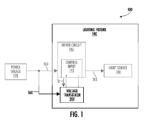
[0033] Referring now to the FIGS., FIG. 1 depicts a lighting system 100
according to
example embodiments of the present disclosure. As shown, the lighting system
100 can include
6
CA 03091129 2020-08-12
WO 2019/160731 PCT/US2019/016953
one or more lighting fixtures 140. In example embodiments, the one or more
lighting fixtures
140 can include a driver circuit 142 and one or more light emitting diode
(LED) light sources
144. Aspects of the present disclosure can be used with other suitable light
sources without
deviating from the scope of the present disclosure.
[0034] In example embodiments, the driver circuit 142 can be configured to
receive AC
input power 160 from a power source 150 and convert the AC input power 160 to
a driver output
162 (e.g., driver current) suitable for powering the one or more LED light
sources 144. The
driver circuit 142 can include various components, such as switching elements
(e.g., transistors).
Gate timing commands can be provided to the one or more switching elements to
convert the AC
input power 160 to the driver output 162.
[0035] According to example aspects of the present disclosure, the one or
more lighting
fixtures 140 can include a voltage transducer 200. In example embodiments, the
voltage
transducer 200 can be configured to provide one or more dimming control
signals to the driver
circuit 142 to control dimming of the one or more LED light sources 144 based
on the magnitude
of the AC input power 160.
[0036] In example embodiments, the driver circuit 142 can adjust the driver
output 162 based
at least in part on a dimming control signal (e.g., OV to 10V dimming control
signal). More
specifically, the dimming control signal can be indicative of a voltage (e.g.,
OV to 10V) at a
control input 143 of the driver circuit 142. For example, reducing the dimming
control signal by
50% can result in a corresponding reduction in the driver output 162. The
reduction of the driver
output 162 can reduce the overall driver current for supply to the one or more
LED light sources
144. As a result, the lumen output of the one or more LED light sources 144
can be adjusted
(e.g., dimmed) by varying the dimming control signal.
[0037] In example embodiments, the driver circuit 142 can provide a control
current ID to the
voltage transducer 200 via the control input 143. The magnitude of the control
current ID can
determine the dimming control signal. For instance, a higher magnitude of the
control current ID
can be associated with a 10 V dimming control signal, whereas a lower
magnitude of the control
current ID can be associated with a 2 V dimming control signal. The voltage
transducer 200 can
be configured to sink the control current ID based, at least in part, on the
magnitude of the AC
input power 160. In this manner, the voltage transducer 200 can adjust the
magnitude of the
dimming control signal to dim or brighten the one or more LED light sources
144.
7
CA 03091129 2020-08-12
WO 2019/160731 PCT/US2019/016953
[0038] FIG. 2 depicts a block diagram of the voltage transducer 200
according to example
embodiments of the present disclosure. As shown, the voltage transducer 200
can include a
power conversion circuit 210, one or more control devices 220, and a current
sink circuit 240.
The power conversion circuit 210 can be configured to receive the AC input
power 160 and
convert the AC input power 160 to direct current (DC) power. More
specifically, the power
conversion circuit 210 can include various electrical components (e.g.,
resistors, capacitors,
diodes, etc.) configured to convert the AC input power 160 to the DC power
164. Alternatively
or additionally, the power conversion circuit 210 can be configured to
determine a sensing input
166 based, at least in part, on the AC input power 160. In example
embodiments, the sensing
input 166 can indicate a magnitude of the AC input power 160. More
specifically, the sensing
input 166 can be a direct current (DC) sensing input.
[0039] The power conversion circuit 210 can provide the DC power 164 and
sensing input
166 to the one or more control devices 220. In example embodiments, the one or
more control
devices 220 can include a microcontroller having one or more processors and
associated memory
devices. More specifically, the one or more control devices 220 can be
configured to provide a
control signal 180 to the current sink circuit 240 based, at least in part, on
the sensing input 166.
[0040] Although FIG. 2 depicts the one or more control devices 220 as being
a component of
the voltage transducer 200, it should be appreciated that the one or more
control devices 220 can
be a component of any suitable component of the lighting fixture 140. For
instance, the control
one or more control devices 220 can, in alternative embodiments, be a
component of the driver
circuit 142. Alternatively, the one or more control devices 220 can be a
standalone component
within the lighting fixture 140.
[0041] Referring now to FIG. 3, a block diagram of components of the power
conversion
circuit 210 is provided according to example embodiments of the present
disclosure. As shown,
the power conversion circuit 210 can include a transformer 212 configured to
convert a first AC
voltage 170 associated with the AC input power 160 (FIG. 1) to a second AC
voltage 172. More
specifically, the transformer 212 can be a step-down transformer, and a
magnitude of the second
AC voltage 172 can be less than a magnitude of the first AC voltage 170.
[0042] As shown, the power conversion circuit 210 can include a rectifier
214 and a voltage
regulator 216. The rectifier 214 can be configured to convert the second AC
voltage 172 to a first
direct current (DC) voltage 174. More specifically, the rectifier 214 can be a
half-wave rectifier
8
CA 03091129 2020-08-12
WO 2019/160731 PCT/US2019/016953
or a full-wave rectifier. The voltage regulator 216 can be configured to
convert the first DC
voltage 174 to a second DC voltage. In example embodiments, the second DC
voltage can be
less than the first DC voltage 174. It should be appreciated that the second
DC voltage can be
associated with the DC power 164 the power conversion circuit 210 provides to
the control
devices 220 (FIG. 3).
[0043] The power conversion circuit 210 can include a sensing circuit 218
configured to
convert the second AC voltage 172 to the sensing input 166 that can be
provided to the one or
more control devices 220 (FIG. 2). As discussed above, the one or more control
devices 220 can
provide the control signal 180 (FIG. 2) to the current sink circuit 240 (FIG.
2) based, at least in
part, on the sensing input 166. As will be discussed below in more detail, the
one or more control
devices 220 can be programmed to generate the control signal 180 according to
one or more
control curves defining a relationship between the sensing input 166 and the
control signal 180.
[0044] Referring now to FIG. 4, example control curves are provided
according to example
aspects of the present disclosure. The control curves can be implemented by
the one or more
control devices 220 (e.g., microcontroller). As shown, FIG. 4 plots a
magnitude of the sensing
input 166 (FIG. 2) along the horizontal axis and a duty cycle of the control
signal 180 (FIG. 2)
along the vertical axis. More specifically, three example control curves 302,
304, and 306 are
depicted. As will be discussed below in more detail, each curve 302, 304, and
306 is defined
based on a relationship between a magnitude of a voltage associated with the
sensing input 166
and a duty cycle of the control signal 180.
[0045] Curve 302 may be defined based on a linear relationship between the
voltage
associated with the sensing input 166 (FIG. 2) and a duty cycle of the control
signal 180 (FIG.
2). In example embodiments, the one or more control devices 220 (FIG. 2) can
be configured to
provide the control signal 180 based on curve 302. In this manner, the one or
more control
devices 220 can be configured to linearly increase or linearly decrease the
duty cycle of the
control signal 180 based on the magnitude of the sensing input 166. For
instance, the one or
more control devices 220 can be configured to linearly increase the duty cycle
of the control
signal 180 as the magnitude of the voltage associated with the sensing input
166 increases.
Conversely, the one or more control devices 220 can be configured to linearly
decrease the duty
cycle of the control signal 180 as the magnitude of the voltage associated
with the sensing input
166 decreases.
9
CA 03091129 2020-08-12
WO 2019/160731 PCT/US2019/016953
[0046] Curve 304 may be defined based on an exponential relationship
between the voltage
associated with the sensing input 166 and the duty cycle of the control signal
180. In this
manner, the one or more control devices 220 can be configured to exponentially
increase or
exponentially decrease the duty cycle of the control signal 180 based on the
magnitude of the
sensing input 166. For instance, the one or more control devices 220 can be
configured to
exponentially increase the duty cycle of the control signal 180 as the
magnitude of the voltage
associated with the sensing input 166 increases. Conversely, the one or more
control devices 220
can be configured to exponentially decrease the duty cycle of the control
signal 180 as the
magnitude of the voltage associated with the sensing input 166 decreases.
[0047] Curve 306 may be defined based on an inverse exponential
relationship between the
voltage associated with the sensing input 166 and the duty cycle of the
control signal 180. In this
manner, the one or more control devices 220 can be configured to exponentially
decrease the
duty cycle of the control signal 180 as the magnitude of the voltage
associated with the sensing
input 166 increases. Conversely, the one or more control devices 220 can be
configured to
exponentially increase the duty cycle of the control signal 180 as the
magnitude of the voltage
associated with the sensing input 166 decreases.
[0048] Referring now to FIG. 5, an example control curve 308 defined based
on a step
function is provided according to example embodiments of the present
disclosure. The control
one or more control devices 220 can be configured to provide the control
signal 180 (FIG. 2)
based on curve 308. In this manner, the one or more control devices 220 can be
configured to
increase the duty cycle of the control signal 180 in an incremental fashion as
the magnitude
associated with the sensing input 166 increases. Conversely, the one or more
control devices
220 can be configured to decrease the duty cycle of the control signal in an
incremental fashion
as the magnitude associated with the sensing input 166 decreases.
[0049] FIG. 6 depicts a block diagram of the current sink circuit 240
according to example
embodiments of the present disclosure. As shown, the current sink circuit 240
can include an
operational amplifier 250 and a switching device 260. The operational
amplifier 250 can include
an inverting input 252, a non-inverting input 254, and an output 256. In
example embodiments,
the control signal 180 can be provided to the non-inverting input 254.
[0050] The switching device 260 can be in operative communication with the
output 256 of
the operational amplifier 250. In example embodiments, the switching device
260 can include
CA 03091129 2020-08-12
WO 2019/160731 PCT/US2019/016953
one or more transistors For example, in some implementations, the transistor
can be a positive-
negative-positive (PNP) bipolar junction transistor. It should be appreciated,
however, that the
switching device 260 can include any suitable type of transistor. For
instance, the switching
device 260 can be a metal-oxide field effect transistor (MOSFET) or other
suitable switching
device.
[0051] The current sink circuit 240 can include a feedback loop 270 coupled
between the
output 256 of the operational amplifier 250 and the inverting input 252 of the
operational
amplifier 250. More specifically, the feedback loop 270 can include a feedback
resistor 272. It
should be appreciated that the feedback resistor 272 can have any suitable
resistance value.
[0052] In example embodiments, the operational amplifier 250 can be
operated as a voltage
comparator. More specifically, the operational amplifier 250 can be configured
to compare a
voltage associated with the control signal 180 and a voltage associated with
the feedback loop
270. When the operational amplifier 250 determines a difference between the
voltage associated
with the control signal 180 and the voltage associated with the feedback loop
270 does not
exceed a threshold, the output 256 of the operational amplifier 250 can
control the switching
device 260 to be in a conducting state. Conversely, the output 256 of the
operational amplifier
250 can control the switching device 260 to be in a non-conducting state when
the difference
between the voltage associated with the control signal 180 and the voltage
associated with the
feedback loop 270 exceeds the threshold.
[0053] In example embodiments, the output 256 of the operational amplifier
250 can control
the switching device 260 to adjust (e.g., increase or decrease) a current
sinking output 190 of the
current sink circuit 240. In some implementations, the current sinking output
190 can be a
dimming control signal received at the control input 143 (FIG. 1) of the
driver circuit 142 (FIG.
1). In this manner, the current sink circuit 240 can control the lumen output
of the LED light
source 144.
[0054] FIG.7 depicts a circuit diagram of the voltage transducer 200
according to example
embodiments of the present disclosure. As shown, the voltage transducer 200
can include a fuse
Fl coupled between the power source 150 (FIG. 1) and the transformer 212.
Alternatively or
additionally, the sensing circuit 218 can include various electrical
components (e.g., resistors,
diodes, capacitors) configured to convert AC power to DC power. More
specifically, the sensing
11
CA 03091129 2020-08-12
WO 2019/160731 PCT/US2019/016953
circuit 218 can include a plurality of resistors (e.g., R1, R2, R3 and R4), a
Schottky diode Di,
and a capacitor Cl configured as shown.
[0055] The rectifier 214 can include various electrical components
configured to convert AC
power to DC power. More specifically, the rectifier 214 can include a Schottky
diode D3, a
resistor R6, and capacitors C5, C8 configured as shown. It should be
appreciated that capacitor
C5 can be polarized (e.g., electrolytic) and capacitor C8 can be non-
polarized.
[0056] The current sink circuit 240 can include a first filter 280 coupled
between the control
device 220 and the operational amplifier 250. More specifically, the first
filter 280 can be a low-
pass filter that includes a resistor R18 and a capacitor C19 coupled between
the resistor R18 and
ground GND. Alternatively or additionally, the current sink circuit 240 can
include a second
filter 282 coupled between the output of the operational amplifier 250 and the
switching device
260. More specifically, the second filter 282 can be a low-pass filter that
includes a resistor R7
and a capacitor C7 coupled between the resistor R7 and ground GND.
[0057] The feedback resistor 272 of the feedback loop 270 corresponds to
resistor R11. As
shown, resistor R11 can be coupled between the switching device 260 and the
inverting input
252 (FIG. 6) of the operational amplifier 250. The current sink circuit 240
can include a resistor
R19 coupled between the inverting input 252 (FIG. 6) and ground GND. In this
manner, resistor
R11 and R19 form a voltage divider.
[0058] The switching device 260 of the current sink circuit 240 is shown as
a PNP transistor.
More specifically, the PNP transistor can include a base input B, an emitter
input E, and a
collector input C. As shown, the base input B can be coupled to the output 256
(FIG. 6) of the
operational amplifier 250 via the second filter 282. The emitter input E can
be coupled to
resistor R11 (e.g., the feedback resistor 272), and the collector input C can
be coupled to ground
GND.
[0059] As shown, the current sink circuit 240 can include a programming
interface 290
communicatively coupled to the one or more control devices 220. In example
embodiments, the
programming interface 290 can include one or more inputs that can be used to
program the one
or more control devices 220. For instance, the one or more inputs can be used
to program the one
or more control devices 220 based on one or more of the control curves
discussed above with
reference to FIGS. 4 and 5.
12
CA 03091129 2020-08-12
WO 2019/160731 PCT/US2019/016953
[0060] Referring now to FIG. 8, a flow diagram of one example method 400
for controlling
operation of a lighting system is provided according to example embodiments of
the present
disclosure. In general, the method 400 will be discussed herein with reference
to the lighting
system 100 described above with reference to FIGS. 1 through 7. However, it
should be
appreciated by those of ordinary skill in the art that the disclosed method
400 can generally be
implemented with lighting systems having any other suitable configuration. In
addition, although
FIG. 8 depicts steps performed in a particular order for purposes of
illustration and discussion,
the method discussed herein is not limited to any particular order or
arrangement. One skilled in
the art, using the disclosure provided herein, will appreciate that various
steps of the method 400
disclosed herein can be omitted, rearranged, combined, and/or adapted in
various ways without
deviating from the scope of the present disclosure.
[0061] At (402), the method 400 can include receiving, at an input of a
voltage transducer, an
alternating current (AC) input power. In example embodiments, the input of the
voltage
transducer can receive the AC input power from a power source, such as a mains
power supply.
[0062] At (404), the method 400 can include receiving, at one or more
control devices, a
sensing input from a power conversion circuit of the voltage transducer. In
example
embodiments, the sensing input can indicate a magnitude of the AC input power.
More
specifically, the sensing input can indicate the magnitude of an AC voltage
associated with the
AC input power.
[0063] At (406), the method 400 can include providing, by the one or more
control devices, a
control signal to a current sink circuit of the voltage transducer based, at
least in part, on the
sensing input. In example embodiments, the control signal can be a PWM signal
having a
variable duty cycle. More specifically, the duty cycle of the PWM signal can
be based, at least in
part, on the sensing input received at (404).
[0064] At (408), the method 400 can include adjusting, by the current sink
circuit, a current
sinking output of the current sinking circuit based, at least in part, on the
control signal. In
example embodiments, adjusting the current sinking output can include
controlling a switching
device of the current sink circuit based, at least in part, on a voltage
associated with the control
signal. For example, controlling operation of the switching device can include
operating the
switching device in a conducting state when a difference between a voltage
associated with the
control signal and a voltage associated with a feedback loop of the current
sink circuit does not
13
CA 03091129 2020-08-12
WO 2019/160731 PCT/US2019/016953
exceed a threshold. Alternatively, controlling operation of the switching
device can include
operating the switching device in a non-conducting state when a difference
between the voltage
associated with the control signal and a voltage associated with a feedback
loop of the current
sink circuit does exceed the threshold.
[0065] At (410), the method 400 can include providing, by the current sink
circuit, the
current sinking output to a driver circuit of the light system. In example
embodiments, the
current sink circuit can provide the current sinking output to a driver
circuit to adjust a driver
output (e.g., a DC voltage) the driver circuit provides to a light source,
such as a LED light
source. More specifically, the current sinking output can be a dimming control
signal (e.g., OV to
V). In this manner, the voltage transducer can dim or brighten the light
source in response to
one or more adjustments made to the AC input power.
[0066] Referring now to FIG. 9, another example of a lighting system 500 is
provided
according to example embodiments of the present disclosure. As shown, several
components of
the lighting system 500 are similar to components of the lighting system 100
depicted in FIG. 1.
For instance, the lighting system 500 includes the driver circuit 142 and
voltage transducer 200.
However, the lighting system 500 of FIG. 9 also includes a current splitter
circuit 510 in
operative communication with the driver circuit 142 and the voltage transducer
200.
Additionally, the lighting fixture 140 of FIG. 9 includes a first LED array
520 and a second LED
array 530.
[0067] As illustrated in FIG. 9, the current splitter circuit 510 can be
configured to convert
the driver output 162 into a first current I for powering the first LED array
520 and a second
current 12 for powering a second LED array 530. In this manner, the current
splitter circuit 510
can be used to adjust the lumen output of the first LED array 520 relative to
the lumen output of
the second LED array 530. The current splitter circuit 510 can be configured
to control the
current ratio of the first current II provided to the first LED array 520 and
the second current 12
provided to the second LED array 530.
[0068] As an example, the first LED array 520 can be associated with a
different color
temperature relative to the second LED array 530. As a variable reference
signal the voltage
transducer 200 provides to the current splitter circuit 510 is adjusted, for
instance, from OV to
by, the current splitter circuit 510 can adjust the ratio of the first current
II provided to the first
LED array 520 relative to the second current 12 provided to the second LED
array 530. In this
14
CA 03091129 2020-08-12
WO 2019/160731 PCT/US2019/016953
manner, the amount of light emitted by the first LED array 520 at a first
color temperature can be
adjusted relative to the amount of light emitted by the second LED array 530
at a second color
temperature, resulting in a different overall color temperature of the light
output of the lighting
system 500.
[0069] As another example, the first LED array 520 can be associated with a
first lighting
direction (e.g. to provide uplighting) and the second LED array 530 associated
with a second
lighting direction (e.g. to provide downlighting). As the variable reference
signal provided to the
current splitter circuit 510 is adjusted, for instance, from OV to I OV, the
current splitter circuit
510 can adjust the ratio of the current provided to the first LED array 520
relative to the current
provided to the second LED array 530. In this manner, the amount of lighting
in the first
direction can be adjusted relative to the amount of lighting in the second
direction to provide
different lighting effects in the lighting system 500.
[0070] Aspects of the present disclosure are discussed with reference to
first and second
LED arrays 520, 530 having different color temperature for purposes of
illustration and
discussion. The first and second LED arrays 520, 530 can include many other
suitable variations
without deviating from the scope of the present disclosure. For instance, the
first and second
LED arrays 520, 530 can be associated with a different brightness, different
lighting direction,
different layout, or other suitable characteristics. Alternatively or
additionally, the first and
second LED arrays 520, 530 can be implemented on the same circuit board or on
different circuit
boards.
[0071] The current splitter circuit 510 can include one or more control
devices (e.g., a
microprocessor, a microcontroller, logic device, etc.) and one or more
switching elements (e.g.,
transistors) in line with each of the first LED array 520 and the second LED
array 530. The one
or more control devices can control the amount of current provided to the
first LED array 520
and the second LED array 530 by controlling the switching elements. The
switching elements
used to control the amount of current provided to the first LED array 520 and
to the second LED
array 530 can be either on the low voltage side of the LED arrays or the high
voltage side of the
LED arrays.
[0072] In example embodiments, the current splitter circuit 510 can adjust
the current ratio
based at least in part on the variable reference signal (e.g., OV to 10 V)
that is received as the
current sinking output 190 (FIG. 2) of the voltage transducer 200.
CA 03091129 2020-08-12
WO 2019/160731 PCT/US2019/016953
[0073] In example embodiments, the current splitter circuit 510 can output
a control current
ID to the voltage transducer 200 via the control input 512. The magnitude of
the control current
ID can determine the variable reference signal. For instance, a higher
magnitude of the control
current ID can be associated with a 10 V variable reference signal, whereas a
lower magnitude of
the control current ID can be associated with, for instance, a 2 V variable
reference signal. The
voltage transducer 200 can be configured to sink the control current ID based,
at least in part, on
the magnitude of the AC input power 160. In this manner, the voltage
transducer 200 can adjust
the variable reference signal based on the magnitude of the AC input power 160
to adjust a
current ratio between the first and second LED arrays 520, 530.
[0074] In particular aspects, the one or more control devices can control
the current provided
to the first LED array 520 and to the second LED array 530 according to a
current ratio control
curve based on the variable reference signal. The current ratio control curve
can be stored in
firmware or stored in a memory accessible by the one or more control devices.
The current ratio
control curve can specify the current ratio of the first current provided to
the first LED array 520
and the second current provided to the second LED array 530 as a function of
at least the
variable reference signal.
[0075] The current ratio control curve can be provided in any suitable
format. For instance,
the current ratio control curve can be provided as a look up table, matrix,
correlation, or other
data specifying the current ratio as a function of at least the variable
reference signal. The current
ratio control curve can be defined based on any desired relationship between
the current ratio and
the variable reference signal. For instance, the current ratio control curve
can be designed as
linear, super-linear, parabolic, logarithmic, asymptotic, exponential, as a
step function, or other
relationship between the current ratio and the variable reference signal,
depending on the desired
performance of the lighting system.
[0076] FIG. 10 depicts the lighting system 100 used in an example
environment according to
example aspects of the present disclosure. The environment can be, for
instance, a building 102.
As shown, the building 102 can define an interior 104 configured to
accommodate a first set of
shelves 110, a second set of shelves 112, and a third set of shelves 114
positioned between the
first set of shelves 110 and the second sets of shelves 112. More
specifically, the first set of
shelves 110 can be spaced apart from the third set of shelves 114 to define a
first aisle or
walkway 120. In this manner, the first aisle 120 can accommodate one or more
consumers
16
CA 03091129 2020-08-12
WO 2019/160731
PCT/US2019/016953
shopping for items on the first set of shelves 110 and/or the third set of
shelves 114.
Additionally, the second set of shelves 112 can be spaced apart from the third
set of shelves 114
to define a second aisle or walkway 122. In this manner, the second aisle 122
can accommodate
one or more consumers shopping for items on the second set of shelves 112
and/or the third set
of shelves 114.
[0077] As shown, the plurality of lighting fixtures 140 can receive the AC
input power 160
from the power source 150, such as the mains power supply for the building
102. In example
embodiments, the AC input power 160 provided to the plurality of lighting
fixtures 140 can be
adjusted (e.g., increased or decreased) via a user-input device 152. For
instance, the user-input
device 152 can include one or more mechanical devices (e.g., switch) of a
control panel.
Alternatively, the user-input device 152 can include a computing device having
one or more
processors and associated memory. More specifically, a user can adjust the AC
input power 160
via a user interface associated with the computing device.
[0078] The example environment of FIG. 10 is provided for purposes of
illustration and
discussion. Those of ordinary skill in the art, using the disclosures provided
herein, will
understand that aspects of the present disclosure can be used in any suitable
lighting application
without deviating from the scope of the present disclosure.
[0079] While the present subject matter has been described in detail with
respect to specific
example embodiments thereof, it will be appreciated that those skilled in the
art, upon attaining
an understanding of the foregoing may readily produce alterations to,
variations of, and
equivalents to such embodiments. Accordingly, the scope of the present
disclosure is by way of
example rather than by way of limitation, and the subject disclosure does not
preclude inclusion
of such modifications, variations and/or additions to the present subject
matter as would be
readily apparent to one of ordinary skill in the art.
17