Note: Descriptions are shown in the official language in which they were submitted.
CA 03092180 2020-08-24
WO 2019/177673 PCT/US2018/063509
COMPUTING SYSTEM WITH SUPERCONDUCTING AND NON-
SUPERCONDUCTING COMPONENTS LOCATED ON A COMMON
SUBSTRATE
BACKGROUND
[0001] Semiconductor based integrated circuits used in electronic devices,
such as digital
processors, include digital circuits based on complimentary metal-oxide
semiconductor
(CMOS) technology. CMOS technology, however, is reaching its limits in terms
of the
device size. In addition, power consumption at high clock speeds by digital
circuits based
on the CMOS technology has increasingly become a limiting factor in high
performance
digital circuits and systems. As an example, servers in a data center are
increasingly
consuming large amounts of power. The consumption of power is partly the
result of
power loss from the dissipation of energy even when the CMOS circuits are
inactive. This
is because even when such circuits are inactive, and are not consuming any
dynamic
power, they still consume power because of the need to maintain the state of
CMOS
transistors.
[0002] An additional approach to the use of processors and related components,
based on
CMOS technology, is the use of superconducting logic-based components and
devices.
Superconducting logic-based components and devices can also be used to process
quantum information, such as qubits. But, even superconducting logic-based
devices,
such as superconducting memories, consume significant amount of power because
of the
need to operate at cryogenic temperatures (e.g., 4 K).
SUMMARY
[0003] In one aspect of the present disclosure, a computing system including a
housing,
where a lower pressure is maintained inside the housing than an atmospheric
pressure
outside the housing is provided. The computing system may further include a
first
substrate, inside the housing, arranged in a first plane having a first
surface and a second
surface parallel to the first plane, where the second surface is opposite to
the first surface,
where a first set of the first plurality of components is attached to the
second surface
towards a first end of the first substrate and where a second set of the
second plurality of
components is attached to the second surface towards a second end of the first
substrate,
where the first end is opposite to the second end, where each of the first
plurality of
components is configured to provide primarily a processor functionality and
where each of
the second plurality of components is configured to provide primarily a
storage
1
CA 03092180 2020-08-24
WO 2019/177673
PCT/US2018/063509
functionality.
[0004] The computing system may further include a second substrate, inside the
housing,
arranged in a second plane above or below the first plane, the second
substrate having a
third surface and a fourth surface parallel to the second plane, where the
fourth surface is
opposite to the third surface, where a third set of the first plurality of
components is
attached to the fourth surface towards a third end of the second substrate and
where a
fourth set of the second plurality of components is attached to the fourth
surface towards a
fourth end of the second substrate, where the third end is opposite to the
fourth end, and
where each of the first substrate and the second substrate comprising a
plurality of circuit
traces for interconnecting at least a subset of the first plurality of the
components with at
least a subset of the second plurality of components.
[0005] The computing system may further include a heat-shield configured to
thermally
separate the first end from the second end of the first substrate and
thermally separate the
third end from the fourth end of the second substrate such that each of the
first plurality of
components is configured to operate at a first temperature and each of the
second plurality
of components is configured to operate at a second temperature greater than
the first
temperature, and where the first temperature is in a range between 2 Kelvin to
77 Kelvin
and wherein the second temperature is in a range between 200 Kelvin to 400
Kelvin.
[0006] In another aspect of the present disclosure, a computing system
comprising
housing, where a vacuum is maintained inside the housing is provided. The
computing
system may further include a first substrate, inside the housing, arranged in
a first plane
having a first surface and a second surface parallel to the first plane, where
the second
surface is opposite to the first surface, where a first set of the first
plurality of components
is attached to the second surface towards a first end of the first substrate
and where a
second set of the second plurality of components is attached to the second
surface towards
a second end of the first substrate, where the first end is opposite to the
second end, where
each of the first plurality of components is configured to provide primarily a
processor
functionality and where each of the second plurality of components is
configured to
provide primarily a storage functionality.
[0007] The computing system may further include a second substrate, inside the
housing,
arranged in a second plane above or below the first plane, the second
substrate having a
third surface and a fourth surface parallel to the second plane, where the
fourth surface is
opposite to the third surface, where a third set of the first plurality of
components is
attached to the fourth surface towards a third end of the second substrate and
where a
2
CA 03092180 2020-08-24
WO 2019/177673
PCT/US2018/063509
fourth set of the second plurality of components is attached to the fourth
surface towards a
fourth end of the second substrate, where the third end is opposite to the
fourth end, and
where each of the first substrate and the second substrate comprising a
plurality of circuit
traces for interconnecting at least a subset of the first plurality of the
components with at
.. least a subset of the second plurality of components.
[0008] The computing system may further include a heat-shield configured to
thermally
separate the first end from the second end of the first substrate and
thermally separate the
third end from the fourth end of the second substrate such that each of the
first plurality of
components is configured to operate at a first temperature and each of the
second plurality
of components is configured to operate at a second temperature greater than
the first
temperature, and where the first temperature is in a range between 2 Kelvin to
77 Kelvin
and where the second temperature is in a range between 200 Kelvin to 400
Kelvin.
[0009] In yet another aspect, the present disclosure relates to a computing
system
including a housing, where a vacuum is maintained inside the housing. The
computing
system may further include a first substrate, inside the housing, arranged in
a first plane
having a first surface and a second surface parallel to the first plane, where
the second
surface is opposite to the first surface, where a first set of the first
plurality of components
is attached to the second surface towards a first end of the first substrate
and where a
second set of the second plurality of components is attached to the second
surface towards
a second end of the first substrate, where the first end is opposite to the
second end, where
each of the first plurality of components is configured to provide primarily a
processor
functionality and where each of the second plurality of components is
configured to
provide primarily a storage functionality, and where a first heat sink is
coupled to the first
substrate to thermally clamp the first substrate.
[00010] The computing system may further include a second substrate, inside
the
housing, arranged in a second plane above or below the first plane, the second
substrate
having a third surface and a fourth surface parallel to the second plane,
where the fourth
surface is opposite to the third surface, where a third set of the first
plurality of
components is attached to the fourth surface towards a third end of the second
substrate
and where a fourth set of the second plurality of components is attached to
the fourth
surface towards a fourth end of the second substrate, where the third end is
opposite to the
fourth end, and where each of the first substrate and the second substrate
comprising a
plurality of circuit traces for interconnecting at least a subset of the first
plurality of the
components with at least a subset of the second plurality of components, and
where a
3
CA 03092180 2020-08-24
WO 2019/177673 PCT/US2018/063509
second heat sink is coupled to the second substrate to thermally clamp the
second
substrate.
[00011] The computing system may further include a heat-shield
configured to
thermally separate the first end from the second end of the first substrate
and thermally
separate the third end from the fourth end of the second substrate such that
each of the first
plurality of components is configured to operate at a first temperature and
each of the
second plurality of components is configured to operate at a second
temperature greater
than the first temperature, and where the first temperature is below 9 Kelvin
and where the
second temperature is in a range between 80 Kelvin to 400 Kelvin.
[00012] This Summary is provided to introduce a selection of concepts in a
simplified form that are further described below in the Detailed Description.
This
Summary is not intended to identify key features or essential features of the
claimed
subject matter, nor is it intended to be used to limit the scope of the
claimed subject
matter.
BRIEF DESCRIPTION OF THE DRAWINGS
[00013] The present disclosure is illustrated by way of example and is
not limited
by the accompanying figures, in which like references indicate similar
elements. Elements
in the figures are illustrated for simplicity and clarity and have not
necessarily been drawn
to scale.
[00014] FIG. 1 shows a computing system including components located on at
least
one common substrate, where the at least one common substrate is inside a
housing, in
accordance with one example;
[00015] FIG. 2 shows a cross-section view of computing system in
accordance with
one example;
[00016] FIG. 3 shows a detailed view of a portion of the computing system
of FIG.
1 in accordance with one example;
[00017] FIG. 4 shows a detailed view of a portion of the computing
system of FIG.
1 in accordance with one example;
[00018] FIG. 5 shows a diagram of a component (superconducting or non-
superconducting) in accordance with one example;
[00019] FIG. 6 shows components (e.g., superconducting components or
non-
superconducting components) bonded to a substrate using solder bumps in
accordance
with one example;
[00020] FIG. 7 shows a cross-section view of a superconducting
component in
4
CA 03092180 2020-08-24
WO 2019/177673 PCT/US2018/063509
accordance with one example; and
[00021] FIG. 8 shows a substrate with a graph showing the variation in
the
temperature along the length of the substrate in accordance with one example.
DETAILED DESCRIPTION
[00022] Examples described in this disclosure relate to computing systems
that
include superconducting components and devices. Certain examples of the
present
disclosure relate to a computing system comprising components operating at
cryogenic
temperatures (e.g., at or below 4 Kelvin) and components operating at non-
cryogenic
temperatures (e.g., at or above 300 Kelvin). In one example, the
superconducting system
is housed in a vacuum assembly. In this example, the superconducting system
may
include one or more superconducting component formed on a substrate. The
superconducting component may include integrated circuit chips mounted on the
substrate.
Superconducting components and devices may use Josephson junctions to
implement the
functionality associated with a circuit. An exemplary Josephson junction may
include two
.. superconductors coupled via a region that impedes current. The region that
impedes
current may be a physical narrowing of the superconductor itself, a metal
region, or a thin
insulating barrier. As an example, the Superconductor-Insulator-Superconductor
(SIS)
type of Josephson junctions may be implemented as part of the superconducting
circuits.
As an example, superconductors are materials that can carry a direct
electrical current
(DC) in the absence of an electric field. Superconductors have a critical
temperature (Tc)
below which they have zero resistance. Niobium, one such superconductor, has a
critical
temperature (Tc) of 9.3 Kelvin degrees. At temperatures below Tc, niobium is
superconductive; however, at temperatures above Tc, it behaves as a normal
metal with
electrical resistance. Thus, in the SIS type of Josephson junction
superconductors may be
niobium superconductors and insulators may be A1203 barriers. In SIS type of
junctions,
the superconducting electrons are described by a quantum mechanical wave-
function. A
changing phase difference in time of the phase of the superconducting electron
wave-
function between the two superconductors corresponds to a potential difference
between
the two superconductors.
[00023] Various superconducting circuits including transmission lines can
be
formed by coupling multiple Josephson junctions by inductors or other
components, as
needed. Microwave pulses can travel via these transmission lines under the
control of at
least one clock. The microwave pulses can be positive or negative or a
combination
thereof. The microwave pulses may have a frequency of up to 10 GHz or higher.
Any
5
CA 03092180 2020-08-24
WO 2019/177673 PCT/US2018/063509
circuit board or other type of structure, such as an interposer with such
superconducting
circuits may be required to support not only the high-frequency microwave
signals but
also direct current (DC) signals.
[00024] Although there are several benefits of superconductivity,
including lower
resistance and better bandwidth characteristics, superconducting materials
need to be
operated at cryogenic temperatures (e.g., 4K). A typical 4K environment may
require
approximately 300 watts of power per watt for cooling; whereas at the non-
cryogenic
temperature (e.g., ambient temperature of approximately 300K), only one wat of
power
per watt may be required. If in a large-scale computing system that is data
processing
intensive hundreds of megawatts of power may be required for the 4K
environment. The
present disclosure describes a computing system that may advantageously
consume less
power by limiting thermal conduction between the 4K side and the 300K side by
co-
locating the components on the same substrate that is further housed inside a
vacuum
chamber. In addition, the use of additional features that lower the thermal
conduction may
further enhance the operational efficiency of such a system. As an example,
thermal
shields may be used to provide for radiation heat transfer.
[00025] FIG. 1 shows a computing system 100 including components
located on at
least one common substrate, where the at least one common substrate is inside
a housing,
in accordance with one example. In this example, housing 102 may be configured
to
maintain a vacuum inside the housing. Thus, several components (e.g.,
processors and
memory) corresponding to computing system 100 are located inside a housing
that
maintains vacuum. Housing 102 may include several substrates (e.g., substrate
104, 106,
and 108). Each of these substrates may be formed using glass or other suitable
materials;
for example, various types of polymers. In one example, the glass material may
be
borosilicate glass. In one example, each of these substrates may be a one-
piece glass
substrate. Housing 102 may further include a 77K thermal shield 112 that may
be
configured to thermally isolate portions of each of the substrates located
inside the 77K
thermal shield 112. 77K thermal shield 112 may be cooled via liquid helium
flowing
through each of the pipes 120 and 122 shown in FIG. 1. Pipes 120 and 122
carrying liquid
helium may be brazed to 77K thermal shield 112. In one example, 77K thermal
shield 112
may be formed using a nickel-iron alloy (e.g., Mu-metal). 77K thermal shield
112 may
further be wrapped into a multi-layer insulation (not shown). This way 77K
thermal shield
112 may effectively provide thermal isolation between the 4K space and the
300K space.
In one example, superconducting components (e.g., Central-Processing Units
(CPUs),
6
CA 03092180 2020-08-24
WO 2019/177673 PCT/US2018/063509
Graphics-Processing Units (GPUs), Artificial Intelligence Processors, Field-
Programmable Gate Arrays (FPGAs), Application-Specific Integrated Circuits
(ASICs),
Application-Specific Standard Products (ASSPs), System-on-a-Chip systems
(SOCs),
Complex Programmable Logic Devices (CPLDs)) may be located towards a first end
of
each of the common substrates (e.g., 104, 106, and 108). The superconducting
components may be configured to provide primarily a processor functionality.
As used
herein the phrase "primarily a processor functionality" may include any
functionality that
is required to implement a processing function. As an example, without
limitation, the
phrase the "primary processor functionality" may include at least one of (or
any
appropriate combination of) a central-processing functionality, a graphics-
processing
functionality, an artificial-intelligence functionality, a gate-array
functionality, a memory
functionality, or a bus-interface-management functionality.
[00026] With continued reference to FIG. 1, the first end may be
maintained at a
temperature that is suitable for allowing the superconducting devices to
operate consistent
with the superconductivity principles. Thus, superconducting components may be
maintained at cryogenic temperatures (e.g., 2K to 77K). This may be
accomplished via
the combination of thermal isolation and cooling via liquid helium or other
such coolants.
As an example, copper sidewalls 130 may be mounted adjacent to superconducting
components. Copper sidewalls 130 may also be cooled via liquid helium flowing
through
pipes (e.g., pipe 120) as shown in FIG. 1. In one example, a system operating
in a
cryogenic environment may require a vacuum to operate properly. In one
example, a
vacuum may relate to a pressure in a range of 10-3 TOIT to 1010 Torr. The use
of the
vacuum ensures that there is no convection and thereby advantageously allowing
components that are operating at very different temperatures to be attached to
the same
substrate. It is to be recognized that the temperature ranges referred to
herein relate to the
temperature of the environment in which these components are operating and not
the
temperature of the components themselves. Thus, references such as the
components are
"operating at" or "maintained at" refer to the temperature of the environment
in which
these components are operating or are being maintained inside.
[00027] Still referring to FIG. 1, in this example, non-superconducting
components
(e.g., CMOS, BiCMOS, or other type of devices that are suitable for operation
without
requiring cryogenic temperatures) may be located towards a second end of each
of the
common substrates (e.g., 104, 106, and 108). In this example, the non-
superconducting
components may comprise memory components, including any of non-volatile or
volatile
7
CA 03092180 2020-08-24
WO 2019/177673 PCT/US2018/063509
memory components. Volatile memory components may include any of the various
types
of random-access memory components, including dynamic random-access memory
(DRAM) components. Non-volatile memory components may include any of various
types of memory components that can store information even when they are not
powered,
including flash-memory components. Non-superconducting components may further
include Field-Programmable Gate Arrays (FPGAs), Application-Specific
Integrated
Circuits (ASICs), Application-Specific Standard Products (AS SPs), System-on-a-
Chip
systems (SOCs), Complex Programmable Logic Devices (CPLDs). Thus, while the
non-
superconducting components may provide primarily a storage functionality, they
may
.. include components, such as ASICs, ASSPs, SOCs, CPLDs, or other types of
controllers
that may coordinate communication between the superconducting components and
the
non-superconducting components and handle control and management of the
storage
devices, including DRAMs. As used herein the phrase "primarily a storage
functionality"
may include any functionality that is required to implement a storage
function. As an
.. example, without limitation, the phrase "primarily a storage functionality"
may include at
least one of (or any appropriate combination of) a memory functionality, gate-
array
functionality, a bus-management functionality, a controller functionality, or
a bus-
interface-management functionality.
[00028] Still referring to FIG. 1, the non-superconducting components
may be
.. maintained at non-cryogenic temperatures (e.g., between 200K to 400K). This
may be
accomplished via the combination of thermal isolation and cooling using water
or some
other coolant. As an example, copper sidewalls 140 may be mounted adjacent to
the non-
superconducting components. Copper sidewalls 140 may also be cooled via water
(or
some other coolant) flowing through pipes (e.g., pipe 142 and pipe 144) as
shown in FIG.
1.
[00029] With continued reference to FIG. 1, superconducting components
and non-
superconducting components may communicate with each other using circuit
traces
formed on the top or the bottom surface of each of the common substrates
(e.g., 104, 106,
and 108). The circuit traces may be formed using a suitable manufacturing
process,
.. including, but not limited to, selective laser sintering, fused deposition
modeling, direct
metal laser sintering, stereolithography, cladding, electron beam melting,
electron beam
direct manufacturing, aerosol jetting, ink jetting, semi-solid freeform
fabrication, digital
light processing, 2 photon polymerization, laminated object manufacturing, 3D
printing, or
other similar manufacturing processes. In one example, the circuit traces may
be made of
8
CA 03092180 2020-08-24
WO 2019/177673
PCT/US2018/063509
niobium (or another suitable superconducting material) in a region of the
substrate that
includes superconducting components. This region may exclude any normal metal,
e.g.,
copper metal. In the other region the circuit traces may be made of both
niobium and
copper (or another suitable metal or metal alloy comprising a superconducting
metal and a
normal metal) that includes the non-superconducting components. By having the
superconducting components and the non-superconducting components communicate
via
the signal traces located on the same substrate may advantageously lower the
latency.
This is because the close proximity of these components may reduce the
latency. In
addition, this may also lower the thermal parasitics. Although FIG. 1 shows a
certain
arrangement of components, substrates, and other component, these could be
arranged in a
different manner. In addition, fewer or additional components, substrates, and
other
components may be present.
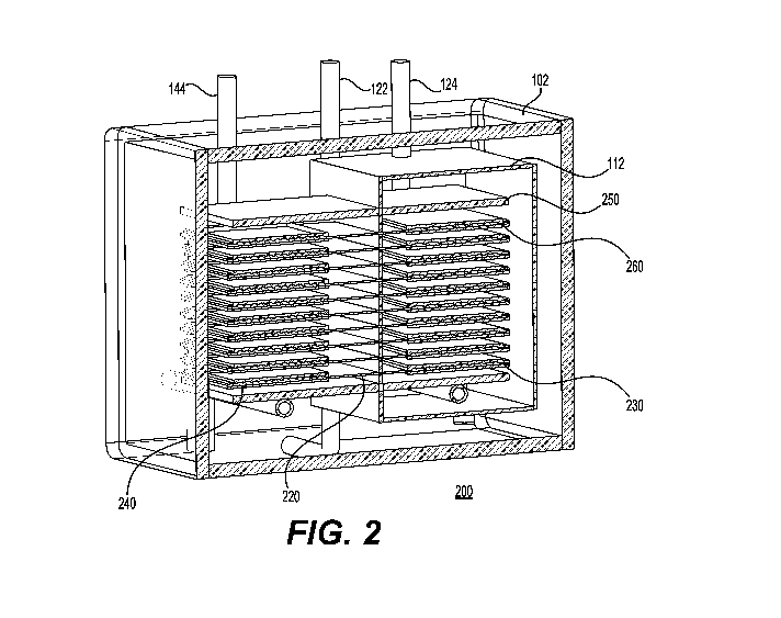
[00030]
Referring now to FIG. 2, a cross-section view 200 of computing system
100 in accordance with one example. The same or similar components that are
shown in
FIG. 2 are referred to with the same reference numerals. In this example,
superconducting
components 230 and non-superconducting components 240 are shown as attached to
a
substrate 220. In one example, the superconducting components may be attached
to each
of the common substrates using any of the various techniques, including flip-
chip bonding.
Similarly, the non-superconducting components may be attached to each of the
common
substrates using any of the various techniques, including flip-chip bonding.
These
components may communicate with each other via signal lines formed in each of
the
common substrates (as described later). Heat shield 112 is used to thermally
separate
superconducting components 230 from non-superconducting components 240. In
this
example, superconducting components 230 are arranged towards the right end of
substrate
220 and non-superconducting components 240 are arranged towards the left end
of
common substrate 220. In this way, the two types of components are thermally
separated
by heat shield 112. Heat shield 112 and other thermal isolation features allow
superconducting components to operate at the cryogenic temperature (e.g.,
below 9 K) and
the non-superconducting components to operate at a substantially higher
temperature (e.g.,
in a range between 10 K to 400 K). FIG. 2 shows additional thermal isolation
components, including for example copper sidewalls 250. In addition, FIG. 2
shows
copper heatsinks, e.g., copper heatsink 260, which is further described later.
Although
FIG. 2 shows a certain number of components arranged in a certain way,
computing
system 100 may include fewer or additional components arranged differently.
9
CA 03092180 2020-08-24
WO 2019/177673 PCT/US2018/063509
[00031] In accordance with one example, FIG. 3 shows a detailed view
300 of a
portion of computing system 100 shown in the cross-section view 200. The
detailed view
300 shows non-superconducting components 310 that may include components that
are
configured to provide primarily a storage functionality. Moreover, as
described earlier,
heat sink 320 and heat sink 330 may be configured to reduce heat radiation
from non-
superconducting components. Each of these heat sinks may be made using copper
or
another appropriate heat conducting metal or alloy. Wedge locks 316 may be
used to
ensure a tight coupling between heat sinks and the substrate including the
components
mounted on the substrate. FIG. 3 additionally shows pipe 312 that may be
brazed to
copper sidewall 130. Certain similar components shown in FIG. 3 are numbered
using the
same reference numerals as in FIG. 1 and FIG. 2. Although FIG. 3 shows a
certain
number of components arranged in a certain way, computing system 100 may
include
fewer or additional components arranged differently.
[00032] In accordance with one example, FIG. 4 shows a detailed view
400 of a
portion of computing system 100 of FIG. 1. As shown in the detailed view 400,
computing system 100 may include substrates 402 and 404 arranged in a housing
described earlier. Substrate 402 is arranged in a plane and has a top surface
460 and a
bottom surface 462. Substrate 404 is arranged in a different plane and also
has a top
surface 470 and a bottom surface 472. In this example, the top surface of each
of the
substrates is opposite to the bottom surface of each of the substrates. In
this example, the
superconducting components 406, 408, and 410 (or the non-superconducting
components)
are attached to a top surface of each of the substrates 402 and 404. In this
example, the
superconducting components may be attached to each of the substrates using an
indium
solder material. Copper heat sinks 454, 456, 466, and 476 may be configured to
provide a
thermal path for removing heat from the superconducting components.
Mechanisms, such
as spring force mechanisms 442, 444, and 446 may be used to push the
superconducting
components (e.g., 406, 408, and 410) into closer contact with copper heat
sinks 466 and
476. In addition, wedge locks (e.g., 452) may be used to clamp the substrates
(e.g.,
substrate 402) to copper sidewalls to provide another thermal path for cooling
the
substrates and the components attached to the common substrates. In this
example, the
components attached to substrates 402 and 404 may be coated or filled with a
thermally-
conductive material (e.g., indium solder) to address the coefficient of
thermal expansion
(CTE) mismatch between the copper heat sinks and the components (e.g., both
superconducting components and non-superconducting components) that are
primarily
CA 03092180 2020-08-24
WO 2019/177673 PCT/US2018/063509
made of silicon. Although FIG. 4 shows a certain number of components arranged
in a
certain way, computing system 100 may include fewer or additional components
arranged
differently.
[00033] FIG. 5 shows a component 500 (e.g., any of the components
earlier) in
accordance with one example. Component 500 may include several dies located in
different positions. Each of dies 504, 506, 508, 510, 512, 514, 516, 518, and
520 may be
connected via signal traces to connectors at the base of component 500 (not
shown).
Those connectors may in turn be connected to solder balls or other attachment
mechanisms for attaching each of the components to the common substrate. In
one
.. example, bump parameters may be different for each position. Signal traces
or lines may
connect chip bumps to the perimeter connections for evaluation and testing of
the
components. Although FIG. 5 shows a certain number of dies arranged in a
certain way,
component 500 may include fewer or additional dies arranged differently.
[00034] FIG. 6 shows a cross-section view of components (e.g.,
superconducting
components or non-superconducting components) bonded to a substrate using
solder
bumps. In this example, component 604 may be bonded to substrate 602 using
indium
bumps 612. Similarly, component 606 may be bonded to substrate 602 using
indium
bumps 614. Finally, component 608 may be bonded to substrate 602 using indium
bumps
616. Although FIG. 6 shows a certain number of components bonded using indium
bumps
to a substrate, other attachment techniques may also be used.
[00035] FIG. 7 shows a cross-section view of a superconducting
component 700 in
accordance with one example. Superconducting component 700 may include a stack
of
superconducting layers and dielectric layers formed on a substrate. In one
example, the
superconducting component may be formed to support signals ranging from DC to
signals
having a frequency that is greater than 10 GHz. In this example, the
superconducting
component may be fabricated over large silicon substrates such as 200 mm
wafers, 300
mm wafers or even larger wafers, which may be separated into multiple dies. In
one
example, the substrate could be made from silicon or any other thermally
insulating or
conducting material. Also, in this example, signal traces and ground planes
may be
formed by sputtering niobium, or a similar superconducting material. As an
example,
compounds of niobium such as niobium nitride (NbN) or niobium titanium nitride
(NbTiN) may also be used. Other physical vapor deposition (PVD) methods, such
as
molecular beam epitaxy (MBE) may also be used. Depending on the type of the
material
used for the traces, sputtering processes, chemical vapor deposition (CVD)
processes,
11
CA 03092180 2020-08-24
WO 2019/177673 PCT/US2018/063509
plasma enhanced chemical vapor deposition (PECVD) process, evaporation
processes, or
atomic layer deposition (ALD) processes may also be used. Thus, for example,
the
niobium compounds such as NbN and NbTiN may be formed using a CVD process.
[00036] With continued reference to FIG. 7, in the example
superconducting
component 700, the dielectric layers could be spin-on polyimide,
Benzocyclobutene
(BCB), liquid crystal polymer (LCP), or some other polymer material. The
superconducting component 700 may further include vias that may be formed by
conformal deposition of the niobium in the same deposition step as the traces
or ground
plane. The via wells could be patterned directly in a photo-imageable
polyimide, or
.. etched in a separate step. The metal traces and vias may be defined in the
same
subtractive etch step. The pad connections may be configured to support Ti/Au
or Ti/A1
pads for a variety of wire bond or flip chip bump and wire bond technologies,
such as
Indium solder bump, Tin-Silver (Snag) solder bump, Gold stud bump, Copper
pillar bump,
or other electrical interconnect bump types.
[00037] Still referring to FIG. 7, superconducting component may include a
dielectric layer 704 formed over a substrate 702. Substrate 702 may be a
silicon substrate,
a sapphire substrate, a glass substrate, or any other suitable substrate.
Dielectric layer 704
may be formed by depositing a dielectric (e.g., liquid crystal polymer (LCP))
on substrate
702. A superconducting layer 706 may be formed over dielectric layer 704.
Superconducting layer 706 may be formed using any of the deposition
techniques, such as
CVD or PECVD, and then patterning the deposited material using
photolithography. In
this example, superconducting layer 706 may be formed by depositing niobium
over
dielectric layer 704. A photo-lithography process may be used to pattern
superconducting
layer 706 to create superconducting wires or other superconducting structures.
Next,
using processes, such as chemical-mechanical polishing, the excess portions of
the
superconducting layer 706 may be removed. In one example, the superconducting
wires
may be formed using niobium or other suitable metals. The layout for the
superconducting structures may be created using a place and route design tool
that is used
to create the layout for the superconducting wires or other elements. As an
example,
photo-resist may be patterned to protect only those areas of superconducting
layer 706 that
will be formed as superconducting wires or other structures as defined by the
layout of the
particular layer, such as a metal layer. Other superconducting metals or metal
alloys may
also be used as part of this step. In one example, the vias and the traces may
be formed by
conformal deposition of niobium in the same deposition step as the one used
for forming
12
CA 03092180 2020-08-24
WO 2019/177673 PCT/US2018/063509
the traces. Niobium may be deposited by sputtering or other similar processes.
Other
physical vapor deposition (PVD) methods, such as molecular beam epitaxy (MBE)
may
also be used. Superconducting component 700 may further include a dielectric
layer 708
formed over a superconducting layer 706. Dielectric layer 708 may be formed by
depositing a dielectric (e.g., liquid polymer) on superconducting layer 706.
In one
example, dielectric layer 708 may be formed by spinning on polyimide on
superconducting layer 706. Another superconducting layer may be formed over
dielectric
layer 708. Vias 710 and 712 may be formed by creating via or contact holes in
dielectric
layer 708 and filling them with niobium or a similar superconducting material.
Additional
superconducting traces including 714, 716, and 718 may be formed as part of
the next
superconducting layer included in the superconducting component. Next, a
dielectric
layer 720 is shown as formed over the superconducting traces or planes (for
example the
superconducting layer including superconducting traces 714, 716, and 718).
Dielectric
layer 720 may be formed by depositing a dielectric (e.g., a liquid polymer) on
the
superconducting layer. In one example, dielectric layer 720 may be formed by
spinning
on polyimide on the superconducting layer. Next, another superconducting layer
may be
formed over dielectric layer 720. Vias may be formed by creating via or
contact holes in
dielectric layer 720 and filling them with niobium or a similar
superconducting material.
Additional superconducting traces including 724, 726, and 728 may be formed as
part of
the next superconducting layer included in the superconducting component. In
one
example, the superconducting wires may be formed using niobium or other
suitable
metals. Yet another dielectric layer 722 is shown as formed over
superconducting traces
or planes (for example the superconducting layer including superconducting
traces 724,
726, and 728). Dielectric layer 722 may be formed by depositing a dielectric
(e.g., a liquid
polymer) on the superconducting layer. In one example, dielectric layer 722
may be
formed by spinning on polyimide on the superconducting layer. Next, vias 730
and 732
and superconducting traces 734, 736, and 738 are shown as formed. In one
example, the
superconducting wires may be formed using niobium or other suitable metals.
Next,
another dielectric layer 740 may be formed. This layer may be formed using
similar
processes as described earlier. Next, vias 742 and 744 and superconducting
traces 750,
752, 754, 756, and 758 are shown as formed. In one example, the
superconducting wires
may be formed using niobium or other suitable metals. Finally, vias764 and 766
are
shown as formed to provide for pad connections. The pad connections may be
configured
to support titanium/gold (Ti/Au) or titanium/aluminum (Ti/A1) pads for a
variety of bump
13
CA 03092180 2020-08-24
WO 2019/177673 PCT/US2018/063509
and wire bond technologies, such as Indium bump, C4 bump, or Copper pillar.
Although
FIG. 7 shows a certain number of layers of the superconducting component 700
arranged
in a certain manner, there could be more or fewer numbers of layers arranged
differently.
In addition, although certain steps are described as being performed in a
certain order,
additional or fewer steps, in a different order may be performed to fabricate
superconducting component 700.
[00038] With continued reference to FIG. 7, in one example,
superconducting layer
106 may be configured to distribute clock signals through the superconducting
component.
The next set of superconducting traces (e.g., superconducting traces 714, 716,
and 718)
may be configured to distribute clock signals through the superconducting
component.
The next set of superconducting traces (e.g., superconducting traces 724, 726,
and 728)
may be configured to act as the ground plane for the superconducting
component. The
next set of superconducting traces (e.g., superconducting traces 734, 736, and
738) may be
configured to distribute signals other than the clock signals through the
superconducting
component. The next set of superconducting traces (e.g., superconducting
traces 750, 752,
754, 756, and 758) may be configured to distribute signals other than the
clock signals
through the superconducting component. Indeed, the functionality of the
various
superconducting layers could be modified based on the requirements associated
with the
superconducting component.
[00039] FIG. 8 shows a substrate 800 with a graph 820 showing the variation
in the
temperature along the length of substrate 800 in accordance with one example.
Substrate
800 includes a substrate layer 802, the non-superconducting component layer
804, the
superconducting component layer 806, and a heat sink 808. In this example, a
thick
(hence highly thermally conductive) copper heat sink 808 is used to effectuate
the
maintenance of a low temperature along a substantial length of the substrate
800. The
component layers may include the chips attached to the substrate layer 802 via
various
mechanisms. The copper heat sink 808 is configured such that the
superconducting
components can be formed as part of the superconducting component layer 806
and the
heat sink 808 does not cover them. Graph 820 shows the variation in the
temperature of
the environment in which the substrate 800 is deployed. Thus, the temperature
on the
processor end is approximately 4K and the temperature on the memory end is
approximately 300K. Despite this variation in temperature along the length of
substrate
800, the various techniques and methodologies described earlier ensure proper
operation
of both the superconducting components and the non-superconducting components.
14
CA 03092180 2020-08-24
WO 2019/177673 PCT/US2018/063509
[00040] In conclusion, in one aspect of the present disclosure, a
computing system
including a housing, where a lower pressure is maintained inside the housing
than an
atmospheric pressure outside the housing is provided. In one example, the
lower pressure
may be in a range between 10-3 TOrr to 1010 Ton.
[00041] The computing system may further include a first substrate, inside
the
housing, arranged in a first plane having a first surface and a second surface
parallel to the
first plane, where the second surface is opposite to the first surface, where
a first set of the
first plurality of components is attached to the second surface towards a
first end of the
first substrate and where a second set of the second plurality of components
is attached to
the second surface towards a second end of the first substrate, where the
first end is
opposite to the second end, where each of the first plurality of components is
configured to
provide primarily a processor functionality and where each of the second
plurality of
components is configured to provide primarily a storage functionality.
[00042] The computing system may further include a second substrate,
inside the
housing, arranged in a second plane above or below the first plane, the second
substrate
having a third surface and a fourth surface parallel to the second plane,
where the fourth
surface is opposite to the third surface, where a third set of the first
plurality of
components is attached to the fourth surface towards a third end of the second
substrate
and where a fourth set of the second plurality of components is attached to
the fourth
surface towards a fourth end of the second substrate, where the third end is
opposite to the
fourth end, and where each of the first substrate and the second substrate
comprising a
plurality of circuit traces for interconnecting at least a subset of the first
plurality of the
components with at least a subset of the second plurality of components. Each
of the
plurality of circuit traces may include a first region including a
superconducting metal but
excluding a normal metal and a second region including both the
superconducting metal
and the normal metal.
[00043] The computing system may further include a heat-shield
configured to
thermally separate the first end from the second end of the first substrate
and thermally
separate the third end from the fourth end of the second substrate such that
each of the first
plurality of components is configured to operate at a first temperature and
each of the
second plurality of components is configured to operate at a second
temperature greater
than the first temperature, and where the first temperature is in a range
between 2 Kelvin
to 77 Kelvin and wherein the second temperature is in a range between 200
Kelvin to 400
Kelvin.
CA 03092180 2020-08-24
WO 2019/177673 PCT/US2018/063509
[00044] The primary processor functionality may include at least one
of a central-
processing functionality, a graphics-processing functionality, an artificial-
intelligence
functionality, a gate-array functionality, a memory functionality, or a bus-
interface-
management functionality. The primary storage functionality may include at
least one of a
memory functionality, gate-array functionality, a bus-management
functionality, a
controller functionality, or a bus-interface-management functionality.
[00045] Each of the first plurality of components may be selected from
a group
comprising a central processing unit, a graphics-processing unit, an
artificial-intelligence
processor, a field-programmable gate array, an application-specific integrated
circuit, an
application-specific standard product, a system-on-a-chip, a complex
programmable logic
device, a random-access memory, and a Josephson magnetic random-access memory.
Each of the second plurality of components may be selected from a group
comprising a
dynamic random-access memory, a field-programmable gate array, an application-
specific
integrated circuit, an application-specific standard product, a system-on-a-
chip, and a
complex programmable logic device.
[00046] In another aspect of the present disclosure, a computing
system comprising
housing, where a vacuum is maintained inside the housing is provided. In one
example,
the vacuum may correspond to a pressure in a range between 10-3 Torr to 10-10
Torr.
[00047] The computing system may further include a first substrate,
inside the
housing, arranged in a first plane having a first surface and a second surface
parallel to the
first plane, where the second surface is opposite to the first surface, where
a first set of the
first plurality of components is attached to the second surface towards a
first end of the
first substrate and where a second set of the second plurality of components
is attached to
the second surface towards a second end of the first substrate, where the
first end is
opposite to the second end, where each of the first plurality of components is
configured to
provide primarily a processor functionality and where each of the second
plurality of
components is configured to provide primarily a storage functionality.
[00048] The computing system may further include a second substrate,
inside the
housing, arranged in a second plane above or below the first plane, the second
substrate
having a third surface and a fourth surface parallel to the second plane,
where the fourth
surface is opposite to the third surface, where a third set of the first
plurality of
components is attached to the fourth surface towards a third end of the second
substrate
and where a fourth set of the second plurality of components is attached to
the fourth
surface towards a fourth end of the second substrate, where the third end is
opposite to the
16
CA 03092180 2020-08-24
WO 2019/177673 PCT/US2018/063509
fourth end, and where each of the first substrate and the second substrate
comprising a
plurality of circuit traces for interconnecting at least a subset of the first
plurality of the
components with at least a subset of the second plurality of components. Each
of the
plurality of circuit traces may include a first region including a
superconducting metal but
excluding a normal metal and a second region including both the
superconducting metal
and the normal metal.
[00049] The computing system may further include a heat-shield
configured to
thermally separate the first end from the second end of the first substrate
and thermally
separate the third end from the fourth end of the second substrate such that
each of the first
plurality of components is configured to operate at a first temperature and
each of the
second plurality of components is configured to operate at a second
temperature greater
than the first temperature, and where the first temperature is in a range
between 2 Kelvin
to 77 Kelvin and where the second temperature is in a range between 200 Kelvin
to 400
Kelvin.
[00050] The primary processor functionality may include at least one of a
central-
processing functionality, a graphics-processing functionality, an artificial-
intelligence
functionality, a gate-array functionality, a memory functionality, or a bus-
interface-
management functionality. The primary storage functionality may include at
least one of a
memory functionality, gate-array functionality, a bus-management
functionality, a
controller functionality, or a bus-interface-management functionality.
[00051] Each of the first plurality of components may be selected from
a group
comprising a central processing unit, a graphics-processing unit, an
artificial-intelligence
processor, a field-programmable gate array, an application-specific integrated
circuit, an
application-specific standard product, a system-on-a-chip, a complex
programmable logic
device, a random-access memory, and a Josephson magnetic random-access memory.
Each of the second plurality of components may be selected from a group
comprising a
dynamic random-access memory, a field-programmable gate array, an application-
specific
integrated circuit, an application-specific standard product, a system-on-a-
chip, and a
complex programmable logic device.
[00052] In yet another aspect, the present disclosure relates to a
computing system
including a housing, where a vacuum is maintained inside the housing. In one
example,
the vacuum may correspond to a pressure in a range between 10-3 Torr to 10-10
Torr.
[00053] The computing system may further include a first substrate,
inside the
housing, arranged in a first plane having a first surface and a second surface
parallel to the
17
CA 03092180 2020-08-24
WO 2019/177673 PCT/US2018/063509
first plane, where the second surface is opposite to the first surface, where
a first set of the
first plurality of components is attached to the second surface towards a
first end of the
first substrate and where a second set of the second plurality of components
is attached to
the second surface towards a second end of the first substrate, where the
first end is
opposite to the second end, where each of the first plurality of components is
configured to
provide primarily a processor functionality and where each of the second
plurality of
components is configured to provide primarily a storage functionality, and
where a first
heat sink is coupled to the first substrate to thermally clamp the first
substrate.
[00054] The computing system may further include a second substrate,
inside the
housing, arranged in a second plane above or below the first plane, the second
substrate
having a third surface and a fourth surface parallel to the second plane,
where the fourth
surface is opposite to the third surface, where a third set of the first
plurality of
components is attached to the fourth surface towards a third end of the second
substrate
and where a fourth set of the second plurality of components is attached to
the fourth
surface towards a fourth end of the second substrate, where the third end is
opposite to the
fourth end, and where each of the first substrate and the second substrate
comprising a
plurality of circuit traces for interconnecting at least a subset of the first
plurality of the
components with at least a subset of the second plurality of components, and
where a
second heat sink is coupled to the second substrate to thermally clamp the
second
substrate.
[00055] The computing system may further include a heat-shield
configured to
thermally separate the first end from the second end of the first substrate
and thermally
separate the third end from the fourth end of the second substrate such that
each of the first
plurality of components is configured to operate at a first temperature and
each of the
second plurality of components is configured to operate at a second
temperature greater
than the first temperature, and where the first temperature is below 9 Kelvin
and where the
second temperature is in a range between 80 Kelvin to 400 Kelvin.
[00056] The primary processor functionality may include at least one
of a central-
processing functionality, a graphics-processing functionality, an artificial-
intelligence
functionality, a gate-array functionality, a memory functionality, or a bus-
interface-
management functionality. The primary storage functionality may include at
least one of a
memory functionality, gate-array functionality, a bus-management
functionality, a
controller functionality, or a bus-interface-management functionality.
[00057] Each of the first plurality of components may be selected from
a group
18
CA 03092180 2020-08-24
WO 2019/177673 PCT/US2018/063509
comprising a central processing unit, a graphics-processing unit, an
artificial-intelligence
processor, a field-programmable gate array, an application-specific integrated
circuit, an
application-specific standard product, a system-on-a-chip, a complex
programmable logic
device, a random-access memory, and a Josephson magnetic random-access memory.
Each of the second plurality of components may be selected from a group
comprising a
dynamic random-access memory, a field-programmable gate array, an application-
specific
integrated circuit, an application-specific standard product, a system-on-a-
chip, and a
complex programmable logic device.
[00058] It is to be understood that the methods, modules, and
components depicted
herein are merely exemplary. For example, and without limitation, illustrative
types of
superconducting devices may include Field-Programmable Gate Arrays (FPGAs),
Application-Specific Integrated Circuits (ASICs), Application-Specific
Standard Products
(ASSPs), System-on-a-Chip systems (SOCs), Complex Programmable Logic Devices
(CPLDs), etc.
[00059] In addition, in an abstract, but still definite sense, any
arrangement of
components to achieve the same functionality is effectively "associated" such
that the
desired functionality is achieved. Hence, any two components herein combined
to achieve
a particular functionality can be seen as "associated with" each other such
that the desired
functionality is achieved, irrespective of architectures or inter-medial
components.
Likewise, any two components so associated can also be viewed as being
"operably
connected," or "coupled," to each other to achieve the desired functionality.
[00060] Furthermore, those skilled in the art will recognize that
boundaries between
the functionality of the above-described operations are merely illustrative.
The
functionality of multiple operations may be combined into a single operation,
and/or the
functionality of a single operation may be distributed in additional
operations. Moreover,
alternative embodiments may include multiple instances of a particular
operation, and the
order of operations may be altered in various other embodiments.
[00061] Although the disclosure provides specific examples, various
modifications
and changes can be made without departing from the scope of the disclosure as
set forth in
the claims below. Accordingly, the specification and figures are to be
regarded in an
illustrative rather than a restrictive sense, and all such modifications are
intended to be
included within the scope of the present disclosure. Any benefits, advantages,
or solutions
to problems that are described herein with regard to a specific example are
not intended to
be construed as a critical, required, or essential feature or element of any
or all the claims.
19
CA 03092180 2020-08-24
WO 2019/177673 PCT/US2018/063509
[00062] Furthermore, the terms "a" or "an," as used herein, are
defined as one or
more than one. Also, the use of introductory phrases such as "at least one"
and "one or
more" in the claims should not be construed to imply that the introduction of
another claim
element by the indefinite articles "a" or "an" limits any particular claim
containing such
introduced claim element to inventions containing only one such element, even
when the
same claim includes the introductory phrases "one or more" or "at least one"
and indefinite
articles such as "a" or "an." The same holds true for the use of definite
articles.
[00063] Unless stated otherwise, terms such as "first" and "second"
are used to
arbitrarily distinguish between the elements such terms describe. Thus, these
terms are not
necessarily intended to indicate temporal or other prioritization of such
elements.