Note: Descriptions are shown in the official language in which they were submitted.
CA 03092214 2020-08-25
1
CHANNEL DEVICE
BACKGROUND OF THE INVENTION
1. Field of the Invention
[0001] The present invention relates to a channel device used for
pharmaceutical research and
the like.
2. Description of the Related Art
[0002] In recent years, it has been attempted to use a channel device having a
channel with a
width of micrometer order called a micro channel as an organ model of a blood
vessel, an
intestinal tract, a liver, a lung, or the like.
[0003] For example, JP2011-528232A discloses a channel device (an
organomimetic device
having a micro channel) including a body which has a central micro channel
(micro channel)
therein and an at least partially porous membrane positioned within the
central micro channel,
in which the porous membrane is configured to separate the central micro
channel to form a
first central micro channel and a second central micro channel, a first fluid
flows through the
first central micro channel and a second fluid flows through the second
central micro channel,
and a plurality of cells (living cells) are fixed to the porous membrane.
[0004] In the channel device, an air, a blood, water, cells, compounds,
particles, a culture
solution, and the like are caused to flow through the first central micro
channel and the second
central micro channel in a state where cells are fixed to the porous membrane.
As a result,
various analyzes can be performed on the porous membrane that reproduces an
organ.
[0005] As an example, by causing a fluorescently labeled large molecule (for
example, a
dextran having a different weight) to flow through a micro channel and
measuring the
fluorescence, permeability of a cell layer formed on a porous membrane can be
evaluated.
In addition, by causing a liquid to flow through a micro channel and imaging
(visualizing) cells on a porous membrane using a transmission electron
microscope,
immunohistocytochemistry, a confocal microscope, or other appropriate means, a
structure of
a cell layer or the like formed on the porous membrane can be evaluated.
Furthermore, by using an electrode, infrared or photodetection means (camera
and
light emitting diode (LED)), magnetic detection means, or the like as a
sensor, a characteristic
and a state of a cell layer or the like formed on a porous membrane can be
monitored. For
example, by measuring electrical characteristics such as a potential
difference, a resistance,
and a short circuit current using an electrode, a transport function of a
fluid and an ion passed
Date Recue/Date Received 2020-08-25
CA 03092214 2020-08-25
2
through a cell layer or the like formed on a porous membrane and formation of
a barrier can be
confirmed.
SUMMARY OF THE INVENTION
[0007] Incidentally, since a human body is complicated, only one measurement
is not enough
to accurately evaluate cells and the like using the channel device. That is,
in order to perform
accurate evaluation of cells and the like using the channel device, for
example, it is preferable
to perform a plurality of kinds of measurement at the same time, such as
simultaneously
performing of imaging of cells on the porous membrane and measurement of a
resistance
value using an electrode, and performing an evaluation based on a plurality of
measurement
results.
[0008] However, it is difficult for the channel device in the related art to
perform a plurality of
kinds of measurement at the same time, in particular, to perform optical
measurement such as
measurement using a fluorescent label and imaging of cells and electrical
measurement using
an electrode at the same time.
[0009] An object of the present invention is to solve the above problems of
the related art, and
is to provide a channel device used as an organ model or the like and capable
of
simultaneously performing optical measurement and electrical measurement.
[0010] In order to solve this problem, the present invention has the following
configuration.
[1] A channel device comprising:
a first channel member having a first channel;
a second channel member having a second channel;
a porous membrane provided between the first channel member and the second
channel member; and
a pair of transparent electrodes provided so as to interpose the first channel
and the
second channel therebetween.
[2] The channel device according to [1],
in which the pair of transparent electrodes is formed of the transparent
electrode in
contact with the first channel and the transparent electrode in contact with
the second channel.
[3] The channel device according to [1] or [2],
in which at least one of the transparent electrodes is a planar electrode.
[4] The channel device according to [3],
in which at least one of the transparent electrodes is a planar electrode
including the
porous membrane in a case of being viewed from a direction orthogonal to a
main surface of
Date Recue/Date Received 2020-08-25
CA 03092214 2020-08-25
3
the first channel member.
[5] The channel device according to any one of [1] to [4],
in the transparent electrode is formed on an entire surface of the first
channel member
on which the first channel is formed.
[6] The channel device according to any one of [1] to [5],
in which the second channel member is a plate member having a through-hole
that
serves as the second channel,
a holding plate that abuts on the second channel member and closes the through-
hole
that serves as the second channel is further provided, and
the transparent electrode is formed on an entire surface of the holding plate
that abuts
on the second channel member.
[7] The channel device according to any one of [1] to [6],
in which the first channel member, or the first channel member and the second
channel member are formed of a polymer material, and
the transparent electrode contains a carbon nanotube.
[8] The channel device according to [6],
in which the holding plate is formed of a polymer material, and the
transparent
electrode formed on the entire surface of the holding plate that abuts on the
second channel
member contains a carbon nanotube.
[9] The channel device according to any one of [1] to [8],
in which the porous membrane has through-holes arranged in a honeycomb form.
[10] The channel device according to any one of [1] to [9],
in which the porous membrane is formed of a polymer material.
[11] The channel device according to any one of [1] to [10],
in which cells are fixed to the porous membrane.
[12] The channel device according to [11],
in which the cells fixed to the porous membrane are cells different between
one
surface and the other surface of the porous membrane.
[0011] According to the channel device of an aspect of the present invention,
it is possible to
simultaneously perform optical measurement and electrical measurement.
BRIEF DESCRIPTION OF THE DRAWINGS
[0012] Fig. 1 is a schematic perspective view showing an overall structure of
an example of a
channel device of an aspect of the present invention.
Date Recue/Date Received 2020-08-25
CA 03092214 2020-08-25
4
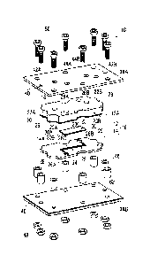
Fig. 2 is a schematic exploded perspective view showing the overall structure
of the
channel device shown in Fig. 1.
Fig. 3 is a schematic plan view showing an example of a porous membrane of the
channel device shown in Fig. 1.
Fig. 4 is a schematic cross-sectional view taken along the line B-B of Fig. 3.
Fig. 5 is a schematic cross-sectional view which is taken along the line A-A
in Fig. 1
and shows the channel device before a channel unit is fixed.
Fig. 6 is a schematic cross-sectional view which is taken along the line A-A
in Fig. 1
and shows the channel device after the channel unit is fixed.
Fig. 7 is a view conceptually showing an example of a measuring method using
the
channel device shown in Fig. 1.
Fig. 8 is a schematic cross-sectional view showing a manufacturing process of
the
channel device shown in Fig. 1.
Fig. 9 is a schematic cross-sectional view showing a manufacturing process of
the
channel device shown in Fig. 1.
Fig. 10 is a schematic cross-sectional view showing a manufacturing process of
the
channel device shown in Fig. 1.
Fig. 11 is a schematic cross-sectional view showing a manufacturing process of
the
channel device shown in Fig. 1.
DESCRIPTION OF THE PREFERRED EMBODIMENTS
[0013] Hereinafter, a cell culture unit of the present invention will be
described in detail based
on preferred embodiments shown in the accompanying drawings.
The embodiments described below exemplify an example of the present invention,
and do not limit the scope of the present invention. In addition, in order to
clarify the
description of each component, the dimension of each component in the drawing
is
appropriately changed. Therefore, the scale in the drawing is different from
the actual one.
[0014] <Channel Unit>
Fig. 1 is a schematic perspective view of an example of a channel device of an
embodiment of the present invention, and Fig. 2 is a schematic exploded
perspective view of
the channel device shown in Fig. 1.
The illustrated example is merely one embodiment of the present invention, and
the
channel device of the embodiment of the present invention is not limited to
this embodiment.
[0015] As shown in Figs. 1 and 2, a channel device 10 has a channel unit 16
including a first
Date Recue/Date Received 2020-08-25
CA 03092214 2020-08-25
channel member 12 and a second channel member 14 that are laminated in a
thickness
direction. In the following description, an upper side in Figs. 1 and 2 is
referred to as
"upper" and a lower side in Figs. 1 and 2 is referred to as "lower". The upper
side in Figs. 1
and 2 is the first channel member 12 side, and the lower side in Figs. 1 and 2
is the second
channel member 14 side.
[0016] A material of the first channel member 12 and the second channel member
14 is
preferably, for example, an elastic transparent material such as
polydimethylsiloxane (PDMS).
As the material forming the first channel member 12 and the second channel
member
14, in addition to PDMS, a polymer material (resin material and polymer) such
as an epoxy
resin, a urethane resin, a styrenic thermoplastic elastomer, an olefinic
thermoplastic elastomer,
an acrylic thermoplastic elastomer, and a polyvinyl alcohol is used.
[0017] Here, a rubber hardness of the first channel member 12 and the second
channel
member 14 is preferably 20 to 80 degrees, and more preferably 50 to 70
degrees.
The "rubber hardness" can be evaluated by measuring a hardness of the first
channel
member 12 and the second channel member 14 with a type A durometer according
to a method
specified in JIS K6253:2012.
[0018] As shown in Fig. 2, on a lower surface of the first channel member 12,
that is, on a
surface 12A facing the second channel member 14, a recessed part 20 that
defines a first
channel 18 (first micro channel 18) is formed. The recessed part 20 has an
inflow port 20A
and an outflow port 20B, and a channel portion 20C that makes the inflow port
20A and the
outflow port 20B communicate with each other. The first channel member 12 is
formed with
through-holes 22A and 22B that penetrate through the first channel member 12
in a thickness
direction and whose lower ends communicate with the inflow port 20A and the
outflow port
20B, respectively. A width and a depth of the first channel 18 (recessed part
20) may be
appropriately set according to a size and application of the channel device
10.
In addition, as will be described later in detail, a first transparent
electrode 60 is
formed (excluding the through-holes) on the entire lower surface of the first
channel member
12 including the recessed part 20 (first channel 18).
[0019] On the other hand, the second channel member 14 is formed with a
through-hole 26
that penetrates through the second channel member 14 in a thickness direction
and defines a
second channel 24 (second micro channel 24). The second channel 24 is formed
by
providing a holding plate 38B, which will be described later, abutting on a
lower surface of the
second channel member 14 (surface opposite to the first channel member 12) to
close a lower
Date Recue/Date Received 2020-08-25
CA 03092214 2020-08-25
6
surface side of the through-hole 26. A width and a depth of the second channel
24
(through-hole 26) may be appropriately set according to a size and application
of the channel
device 10.
The through-hole 26 has an inflow port 26A and an outflow port 26B, and a
channel
portion 26C that makes the inflow port 26A and the outflow port 26B
communicate with each
other.
[0020] Here, the inflow port 26A and the outflow port 26B of the second
channel member 14
are provided at positions that do not overlap the inflow port 20A and the
outflow port 20B of
the first channel member 12 in a planar view. On the other hand, the channel
portion 26C of
the second channel member 14 is provided at a position overlapping the channel
portion 20C
of the first channel member 12 in a planar view.
The planar view, in other words, refers to a case where the channel device 10
of the
embodiment of the present invention is viewed from a direction orthogonal to a
main surface
of the first channel member 12. In addition, the main surface refers to a
largest surface of a
sheet-shaped material, a plate-shaped material, a film-shaped material, or the
like.
[0021] The first channel member 12 is formed with through-holes 28A and 28B
that penetrate
through the first channel member 12 in a thickness direction and whose lower
ends
communicate with the inflow port 26A and the outflow port 26B of the second
channel
member 14.
Further, a recessed part 29 is provided on an outer peripheral surface (side
surface) of
the channel unit 16 (first channel member 12 and second channel member 14) at
a position
where a spacer 46 which will be described later is disposed.
[0022] <Porous Membrane>
A porous membrane 30 is disposed between facing surfaces 12A and 14A of the
first
channel member 12 and the second channel member 14. The porous membrane 30 is
formed
of, for example, a polymer material, and particularly preferably formed of a
hydrophobic
polymer material that can be dissolved in a hydrophobic organic solvent. The
hydrophobic
organic solvent is a liquid having a solubility in water at 25 C of 10 (g/100
g water) or less.
[0023] Examples of the polymer material include polystyrene, polyacry late,
polymethacrylate,
polyacrylamide, polymethacrylamide, polyvinyl chloride, polyvinylidene
chloride,
polyvinylidene fluoride, polyhexafluoropropene, polyvinyl ether,
polyvinylcarbazole,
polyvinyl acetate, polytetrafluoroethylene, polyester, polylactone, polyamide
and polyimide,
polyurethane, poly urea, poly b utadiene, polycarbonate, polyaromatics,
polysulfone,
Date Recue/Date Received 2020-08-25
CA 03092214 2020-08-25
7
polyethersulfone, a polysiloxane derivative, and cellulose acylate.
Examples of polyester include polyethylene terephthalate, polyethylene
naphthalate,
polyethylene succinate, polybutylene succinate, polylactic acid, and poly-3-
hydroxybutyrate.
Examples of polylactone include polycaprolactone and the like. Examples of
polyamide and
polyimide include nylon and polyamic acid. Examples of cellulose acylate
include triacetyl
cellulose, cellulose acetate propionate, and cellulose acetate butyrate.
[0024] These polymer materials may be homopolymers, copolymers, polymer
blends, polymer
alloys, and the like, as necessary, from a viewpoint of a solubility in a
solvent, an optical
property, an electrical property, a film hardness, an elasticity, or the like.
In addition, these
polymer materials may be used alone or in combination of two or more. A
material of the
porous membrane 30 is not limited to the polymer material, and various
materials can be
selected from a viewpoint of cell adhesiveness.
[0025] An upper surface 30A and a lower surface 30B of the porous membrane 30
have a size
that substantially covers the channel portions 20C and 26C of the first
channel 18 and the
second channel 24.
The porous membrane 30 is provided so as to cover the first channel 18 and the
second channel 24. Thereby, the porous membrane 30 separates the first channel
18 and the
second channel 24 from each other.
[0026] Specifically, the upper surface 30A of the porous membrane 30, that is,
a main surface
facing the first channel member 12 defines the first channel 18 together with
the recessed part
20 of the first channel member 12.
The lower surface 30B of the porous member 30, that is, a main surface facing
the
second channel member 14 defines the second channel 24 together with the
through-hole 26 of
the second channel member 14.
[0027] As shown in Figs. 3 and 4, a plurality of through-holes 32 that
penetrate through the
porous membrane 30 in a thickness direction are formed in the porous membrane
30, and
openings 32A of the through-holes 32 are provided on the upper surface 30A and
the lower
surface 30B of the porous membrane 30. As shown in Fig. 3, the opening 32A has
a circular
shape in a planar view. The openings 32A are provided to be spaced from each
other, and a
flat portion 34 extends between the openings 32A adjacent to each other. The
opening 32A is
not limited to a circular shape, and may have a polygonal shape, an elliptical
shape, an
irregular shape, or the like.
[0028] A plurality of the openings 32A are regularly arranged. In the present
invention, as an
Date Recue/Date Received 2020-08-25
CA 03092214 2020-08-25
8
example, the openings 32A are arranged in a honeycomb form.
The arrangement in a honeycomb form is an arrangement in which a parallel
hexagon
or a shape close to this is taken as a unit and centers of the openings 32A
are located at
vertices and an intersection of diagonal lines of these figures. The parallel
hexagon is
preferably a regular hexagon.
Here, the "center of the opening" means the center of the opening 32A in a
planar
view.
[0029] The arrangement of the openings 32A is not limited to the honeycomb
form, and may
be a lattice form or a face-centered lattice form. The arrangement in a
lattice form is an
arrangement in which a parallelogram or a shape close to this is taken as a
unit and the centers
of the openings are located at vertices of these figures. The arrangement in a
face-centered
lattice form is an arrangement in which a parallelogram or a shape close to
this is taken as a
unit and the centers of the openings are located at vertices and an
intersection of diagonal lines
of these figures. In the above description, the parallelogram includes a
square, a rectangle,
and a rhombus, and a square is preferable.
It is preferable that the openings 32A be arranged in a honeycomb form in
order to
easily achieve the following opening ratio.
[0030] In the porous membrane 30, a variation coefficient of an opening
diameter of the
opening 32A is preferably 10% or less, and the smaller the better. The smaller
the variation
coefficient of the opening diameter, the more uniformly red blood cells and
the like can pass
through the plurality of through-holes 32 of the porous membrane 30.
In addition, an opening ratio (void volume) of the porous membrane 30 is
preferably
50% or more. By setting the opening ratio to 50% or more, it is possible to
prevent the
movement of red blood cells and the like from being blocked by the porous
membrane 30. In
a case where the void volume is too large, a strength of the porous membrane
30 is insufficient
with respect to a required strength, and thus the void volume is preferably
95% or less.
Here, the "opening ratio" refers to a ratio of V2 to V1 in percentage in a
case where
VI is a unit volume of the porous membrane 30 in a case where it is assumed
that a main
surface of the porous membrane 30 is smooth, that is, there is no opening 32A,
V2 is a sum of
volumes of the through-hole 32 and a communication hole 36 provided per unit
volume, and
units of V1 and V2 are the same.
[0031] As shown in Fig. 4, the through-hole 32 of the porous membrane 30 has a
spherical
trapezoidal shape in which an upper end and a lower end of a sphere are cut
off. The
Date Recue/Date Received 2020-08-25
CA 03092214 2020-08-25
9
through-holes 32 adjacent to each other communicate with each other by the
communication
hole 36 inside the porous membrane 30.
[0032] It is preferable that one through-hole 32 communicate with all adjacent
through-holes
32. As in the present invention, in a case where the openings 32A of the
plurality of
through-holes 32 are arranged in a honeycomb form, it is preferable that one
through-hole 32
communicate with six adjacent through-holes 32 by six communication holes 36,
respectively.
The through-hole 32 may have a barrel shape, a columnar shape, a polygonal
column
shape, or the like, and the communication hole 36 may be a cylindrical void
that connects the
adjacent through-holes 32 to each other.
[0033] Examples of a method of manufacturing the porous membrane 30 having the
through-holes 32 include a nano-printing method, a condensation method, an
etching method,
a sandblasting method, and a press molding method.
The nano-printing method is a method of manufacturing the through-holes 32 by
pouring a material forming the porous membrane 30 into a mold having an uneven
shape or
pressing the mold against the material forming the porous membrane 30. The
condensation
method is a method in which a surface of the material forming the porous
membrane 30 is
condensed to form the through-holes 32 using a water droplet as a mold.
[0034] As compared with the other methods, in the condensation method, a film
thickness of
the porous membrane 30 can be reduced, a void volume and an opening ratio of
the opening
32A can be increased, and the communication hole 36 can be provided in the
porous
membrane 30. Therefore, in the present invention, the porous membrane 30 is
manufactured
by the condensation method.
Details of the condensation method are described in, for example, JP4945281B,
JP5422230B, JP2011-074140A, and JP5405374B.
[0035] In the channel device 10 of the embodiment of the present invention,
the porous
membrane is not limited to those having such through-holes, and various kinds
of known
porous membranes (porous materials) such as non-woven fabrics and membranes
having
three-dimensional voids can be used.
[0036] In the channel device 10 of the embodiment of the present invention, it
is preferable
that at least a region where cells are seeded on the main surface of the
porous membrane 30 be
coated with at least one selected from the group consisting of fibronectin,
collagen, laminin,
vitronectin, gelatin, perlecan, nidogen, proteoglycan, osteopontin, tenascin,
nephronectin,
basement membrane matrix, and polylysine. Examples of collagen include type I
collagen,
Date Recue/Date Received 2020-08-25
CA 03092214 2020-08-25
type IV collagen, and type V collagen.
By coating the porous membrane 30 with these materials, it is possible to
enhance cell
adhesiveness.
[0037] In a case where the channel device 10 of the embodiment of the present
invention is
used as an organ simulator (organ model) or the like, the main surface of the
porous membrane
30 may have a cell layer that constitutes an organ to be simulated.
The main surface of the porous membrane 30 have the cell layer, whereby the
inside
of the first channel 18 and the inside of the second channel 24 can be made to
have an
environment close to the inside of the organ to be simulated.
That is, the channel device of the embodiment of the present invention may be
a cell
culture device for culturing cells, or may be a channel device for measurement
that has a cell
layer and performs measurement for evaluating cells and/or drug solutions.
[0038] Examples of the cells provided on the main surface of the porous
membrane 30 include
parenchymal cells, stromal cells, muscle cells, fibroblasts, nerve cells,
endothelial cells,
epithelial cells, and cells that differentiate into any of these.
Examples of the parenchymal cells include hepatic parenchymal cells and
pancreatic
parenchymal cells. Examples of the stromal cells include pericytes. Examples
of the
muscle cells include smooth muscle cells, cardiomyocytes, and skeletal muscle
cells.
Examples of the endothelial cells include vascular endothelial cells and
lymphatic endothelial
cells. Examples of the epithelial cells include alveolar epithelial cells,
oral epithelial cells,
bile duct epithelial cells, intestinal epithelial cells, pancreatic duct
epithelial cells, renal
epithelial cells, renal tubular epithelial cells, and placental epithelial
cells. Examples of the
cells that differentiate into any of these include progenitor cells,
mesenchymal stem cells, and
pluripotent stem cells.
[0039] Examples of the pluripotent stem cells include embryonic stem cells (ES
cells),
induced pluripotent stem cells (iPS cells), embryonic germ cells (EG cells),
embryonal
carcinoma cells (EC cells), multipotent adult progenitor cells (MAP cells),
adult pluripotent
stem cells (APS cells), and multi-lineage differentiating stress enduring
cells (Muse cells).
[0040] As cells, cells having gene mutation and/or cells derived from a
patient may be used for
the purpose of reproducing a pathological condition.
[0041] The cell layer provided on the main surface of the porous membrane 30
may have the
same cell layer on both surfaces, or may have cell layers different from each
other on each
surface.
Date Recue/Date Received 2020-08-25
CA 03092214 2020-08-25
11
As an example, a vascular endothelial cell layer is provided on one surface of
the
porous membrane 30 and a smooth muscle cell layer is provided on the other
surface of the
porous membrane 30, whereby the channel device 10 serving as a vascular wall
model can be
obtained.
[0042] <Holding Plate>
As shown in Figs. 1 and 2, the channel device 10 has a holding plate 38A on
the
upper side (first channel member 12 side) and a holding plate 38B on the lower
side (second
channel member 14 side) as a holding member that holds the channel unit 16 in
a compressed
state in a thickness direction.
The holding plate 38A and the holding plate 38B are provided separately from
the
channel unit 16 at both ends of the channel unit 16 in a thickness direction,
that is, on the
upper side of the first channel member 12 and the lower side of the second
channel member 14,
and have a size that covers the entire upper surface of the first channel
member 12 and the
entire lower surface of the second channel member 14.
[0043] Both the holding plate 38A and the holding plate 38B are preferably
formed of a rigid
and transparent polymer material.
Accordingly, examples of a constituent material of the holding plate 38A and
the
holding plate 38B include cycloolefin polymer, acrylic, polycarbonate,
polystyrene, and
polyethylene terephthalate. In addition, the holding plate 38A and the holding
plate 38B are
preferably harder than the first channel member 12 and the second channel
member 14
described above, and further, a rubber hardness is preferably 80 degrees or
more, and more
preferably 90 degrees or more.
[0044] As shown in Fig. 2, a plurality of bolt holes 40 penetrating in a
thickness direction are
formed at positions corresponding to each other on the holding plate 38A and
the holding plate
38B. The number of bolt holes 40 is eight in the illustrated example. The
holding plate
38A provided on the upper side of the first channel member 12 has through-
holes 42A, 42B,
44A, and 44B that communicate with the through-holes 22A, 22B, 28A,and 28B of
the first
channel member 12, respectively.
[0045] Tubes (not shown) are connected to the through-holes 42A, 42B, 44A, and
44B,
respectively, and a solution, a cell suspension, or the like flows into the
first channel 18 and
the second channel 24 through the tubes, and the solution, the cell
suspension, or the like flows
out from the first channel 18 and the second channel 24.
[0046] A plurality of the spacers 46 that define intervals between the holding
plates 38 are
Date Recue/Date Received 2020-08-25
CA 03092214 2020-08-25
12
provided outside the recessed part 29 of the channel unit 16 between a pair of
the holding
plates 38. The number of spacers 46 is eight in the illustrated example. The
spacers 46 are
cylindrical members having an inner diameter substantially the same as an
inner diameter of
the bolt hole 40, and are disposed at positions corresponding to the bolt
holes 40, respectively.
[0047] As shown in Figs. 5 and 6, the pair of holding plates 38 are joined to
each other by a
plurality of bolts 50 that are inserted through the bolt holes 40 and the
spacers 46 and fixed by
nuts 48. In this case, the first channel member 12 and the second channel
member 14 are
compressed and held by the pair of holding plates 38 with the porous membrane
30 interposed
therebetween.
[0048] <Transparent Electrode>
In the channel device 10 of the embodiment of the present invention, a second
transparent electrode 62 is disposed on the holding plate 38B that abuts on
the second channel
24 so as to cover an entire surface abutting on the second channel member 14.
As described
above, the second channel 24 is formed by the holding plate 38B abutting on
the lower surface
of the second channel member 14 and closing the lower surface of the through-
hole 26.
Accordingly, the lower surface side of the second channel 24 is the second
transparent
electrode 62, that is, the second transparent electrode 62 is in contact with
the second channel
24.
As described above, the lower surface of the first channel member 12 has the
recessed
part 20 that defines the first channel 18. The first transparent electrode 60
is provided on the
lower surface of the first channel member 12 so as to cover the entire surface
including the
recessed part 20. That is, the first transparent electrode 60 is in contact
with the first channel
18.
In the channel device 10, a pair of transparent electrodes (electrode pair) is
configured
by the first transparent electrode 60 in contact with the first channel 18 and
the second
transparent electrode 62 in contact with the second channel 24.
[0049] The channel device 10 of the embodiment of the present invention has
the first
transparent electrode 60 and the second transparent electrode 62 as described
above, so that
optical measurement and electrical measurement can be performed at the same
time.
[0050] As described above, since a human body is complicated, only one type of
measurement
is not enough to accurately evaluate cells and the like using the channel
device, and it is
preferable to perform so-called multi-validation in which a plurality of types
of measurements
are performed at the same time.
Date Recue/Date Received 2020-08-25
CA 03092214 2020-08-25
13
As an example of the measurement using the channel device, as shown
conceptually
in Fig. 7, evaluation of permeability of a membrane in which a fluorescently
labeled large
molecule is caused to flow through the first flow channel 18 or the second
flow channel 24,
excitation light is emitted from a light source 70, and fluorescence is
measured by an optical
sensor 72 is exemplified.
In addition, by causing a liquid to flow through the first channel 18 and/or
the second
channel 24 and imaging (visualizing) the cell layer or the like formed on the
porous membrane
30 using an imaging camera 74 such as a transmission electron microscope and a
fluorescence
microscope, a structure of the cell layer or the like can be evaluated.
Furthermore, by connecting an electric sensor 76 to the first transparent
electrode 60
and the second transparent electrode 62 and measuring electrical
characteristics such as a
potential difference, a resistance, and a short circuit current, a transport
function of a fluid and
an ion passed through a membrane and formation of a barrier can be evaluated.
[0051] However, in the channel device in the related art, in a case where
electrodes are formed
corresponding to a first channel and a second channel in order to measure
electrical
characteristics of a cell layer and the like formed on a porous membrane, the
electrodes are
usually formed of a metal, and thus the electrodes act as a like-shielding
member, and optical
measurement and evaluation such as fluorescence measurement and imaging of the
cell layer
cannot be properly performed.
Therefore, the channel device in the related art cannot perform an electrical
measurement and an optical measurement at the same time.
[0052] With respect to this, in the channel device 10 of the embodiment of the
present
invention, a pair of the first transparent electrode 60 and the second
transparent electrode 62 is
provided so as to interpose the first channel 18 and the second channel 24
therebetween.
In the channel device 10 of the embodiment of the present invention, even
though the
pair of electrodes is provided so as to interpose the first channel 18 and the
second channel 24
therebetween, the electrodes are transparent electrodes, and thus the
electrodes do not interfere
with optical measurement methods such as fluorescence measurement and imaging
of the cell
layer. Therefore, according to the channel device 10 of the embodiment of the
present
invention, electrical measurement and optical measurement such as fluorescence
measurement
using the light source 70 and the optical sensor 72 as shown in Fig. 7,
imaging of the cell layer
using the imaging camera 74, and resistance measurement using the electric
sensor 76 can be
performed at the same time.
Date Recue/Date Received 2020-08-25
CA 03092214 2020-08-25
14
In addition, since the transparent electrode is used, even though the
electrode is a
planar electrode, it does not interfere with optical measurement. Therefore,
stable electrical
measurement can be performed with an electrode having a sufficient area.
Furthermore, it is
also possible to extract an electrical property of the surface of the cell
layer formed on the
porous membrane 30 as an electrical signal.
[0053] In the channel device 10 of the embodiment of the present invention,
the first
transparent electrode 60 and the second transparent electrode 62 are
transparent electrodes
having conductivity.
In the present invention, the term "having conductivity" means that a sheet
resistance
value is 0.1 to 10,000 fl/o (Ohms per Square (C2Jsq)), and includes what is
generally called an
electric resistance layer. In a general-purpose power source is used, a lower
sheet resistance
value is preferable, specifically, 300 0/o or less is preferable, 200 n/0 or
less is more
preferable, and 100 0/o or less is still more preferable. In the present
invention, a sheet
resistance value (surface resistivity) may be measured according to Japanese
Industrial
Standards (JIS) K 7194.
In addition, in the present invention, the term "transparent" means that a
transmittance is 60% to 99.99%. A transmittance of the transparent electrode
is preferably
75% or more, more preferably 80% or more, and still more preferably 90% or
more. In the
present invention, for a transmittance, a total light transmittance [%] may be
measured
according to JIS K 7361-1.
[0054] In the channel device 10 of the embodiment of the present invention,
materials of the
first transparent electrode 60 and the second transparent electrode 62 are not
limited, and
various materials used as transparent electrodes in various electronic devices
(electronic
devices, electronic elements) can be used.
Specifically, examples of the materials included in the first transparent
electrode 60
and the second transparent electrode 62 include a metal oxide, a carbon
nanotube, graphene, a
polymer conductor, a metal nanowire, and a metal mesh. Examples of the metal
oxide
include indium tin oxide (ITO) and the like. Examples of the carbon nanotube
include a
carbon nanotube (CNT) and a carbon nanobud (CNB). Examples of the polymer
conductor
include polyacetylene, polypyrro le, polyphenol, poly
aniline, and
polyethylenedioxythiophene/polystyrene sulfonic acid (PEDOT/PSS). Examples of
the metal
nanowire include a silver nanowire and a copper nanowire. Examples of the
metal mesh
include a silver mesh and a copper mesh.
Date Recue/Date Received 2020-08-25
15
A transparent electrode having the metal mesh is preferably formed of a
conductive fine
particle such as silver and copper dispersed in a matrix, rather than a
transparent electrode formed
of only a metal, from a viewpoint of a heat shrinkage rate.
[0055] A transparent electrode formed of these materials may be formed by a
known method
according to the material.
For example, in a case of a transparent electrode containing a carbon
nanotube, the
transparent electrode may be formed by a coating method in which a coating
material in which a
carbon nanotube is dispersed is prepared, the prepared coating material is
applied to a portion
where the transparent electrode is to be formed such as the lower surface of
the first channel
member 12 and dried, and further heat-treated as necessary.
In a case of a transparent electrode containing a carbon nanobud, similarly,
the
transparent electrode may be formed on a portion where the transparent
electrode is to be formed
such as the lower surface of the first channel member 12 by a direct dry
printing (DDP) method
described on page 1012 of 2015 SID International Symposium: Digest of
Technical Papers: June
2015: Display Week 2015: Jun 2015, San Jose, CA, from SID International
Symposium Digest of
Technical Papers; 46, published at Campbell, CA, by Society for Information
Display in 2015.
Furthermore, in a case of a transparent electrode containing a silver
nanowire, similarly,
the transparent electrode may be formed on a portion where the transparent
electrode is to be
formed such as the lower surface of the first channel member 12 by a method
described in
Example 1 of US2013/0341074A.
[0056] Here, in the channel device 10 of the embodiment of the present
invention, both the first
channel member 12 on which the first transparent electrode 60 is formed and
the holding plate 38B
on which the second transparent electrode 62 is formed are preferably formed
of a polymer
material.
In consideration of this point, the material forming the first transparent
electrode 60 and
the second transparent electrode 62 is preferably a material that can be
formed by the coating
method rather than a vapor phase film-forming method (vapor phase depositing
method) such as
plasma chemical vapor deposition (CVD), sputtering, and vacuum deposition.
Among them, a
carbon nanotube is preferably exemplified. In addition, in the channel device
10 of the
embodiment of the present invention, as described above, observation of
fluorescence and the like
is also available, but among metal materials such as metal oxides, there is a
material that emits
light by absorbing excitation light and/or fluorescence. Also in this point, a
carbon nanotube that
does not absorb excitation light and/or fluorescence is preferable as the
material of the transparent
electrode.
Date Recue/Date Received 2022-11-29
CA 03092214 2020-08-25
16
[0057] As will be described later, in the channel device of the embodiment of
the present
invention, the transparent electrode is not limited to the configuration in
which the transparent
electrode is formed on the entire lower surface of the first channel member 12
and the entire
surface of the holding plate 38B as in the present invention.
[0058] Various shapes and sizes of the transparent electrode are available.
Accordingly, the
transparent electrode may be linear or planar, but for reasons described
above, it is preferable
that at least one transparent electrode, preferably both transparent
electrodes, be a planar
electrode. This allows a stable electrical measurement with an electrode
having a sufficient
area.
In the present invention, the planar electrode refers to an electrode having
an area
larger than an area of a region where the first channel 18 and the second
channel 24 are
separated from each other by the porous membrane 30.
It is preferable that at least one transparent electrode, preferably both
transparent
electrodes, have a shape and a size that include the porous membrane 30 in a
case of being
viewed from a direction orthogonal to the main surface of the first channel
member 12. A
case of being viewed from a direction orthogonal to the main surface of the
first channel
member 12 is the same as the above-described planar view. In particular, it is
preferable that
the transparent electrode, such as the first transparent electrode 60, which
abuts on the porous
membrane 30 have such a configuration, so that it is possible to extract the
electrical property
of the surface of the cell layer or the like formed on the porous membrane 30.
[0059] <Method of Manufacturing Channel Device>
In a case where the channel device 10 of embodiment of the present invention
is
manufactured, first, the porous manufacturing 30 having the main surface
attached with a
sterilized paper is prepared. Then, a sterilized paper on the lower surface
30B of the porous
membrane 30 is peeled off by tweezers, and as shown in Fig. 8, the porous
membrane 30 is
placed on the second channel member 14 in which the through-hole 26 is formed
and the
porous membrane 30 and the second channel member 14 are joined to each other.
[0060] Next, a sterilized paper on the upper surface 30A of the porous
membrane 30 is peeled
off by tweezers, the position of the second channel member 14 is aligned with
the position of
the first channel member 12 on which the first channel member 60 is formed
while being
checked with a microscope, and as shown in Fig. 9, the first channel member 12
in which the
recessed part 20 is formed is laminated on the porous membrane 30. Thereby,
the first
channel 18 is defined by the recessed part 20 of the first channel member 12
and the porous
Date Recue/Date Received 2020-08-25
CA 03092214 2020-08-25
17
membrane 30. The first channel 18 is in contact with the first transparent
electrode 60
formed on the first channel member 12.
[0061] Next, as shown in Fig. 10, the holding plate 38A is placed on the upper
surface of the
first channel member 12 while aligning the positions of the through-holes 22A
and 22B with
the positions of the through-holes 42A and 42B, respectively.
After that, the channel unit 16 is turned over, and the holding plate 38B on
which the
second transparent electrode 62 is formed is placed on the lower surface of
the second channel
member 14. Thereby, the second channel 24 is defined by the through-hole 26 of
the second
channel member 14, the porous membrane 30, and the holding plate 38B. The
second
channel 24 is in contact with the second transparent electrode 62 formed on
the holding plate
38B.
[0062] Finally, as shown in Fig. 11, the spacer 46 is disposed around the
channel unit 16, and
the holding plate 38A and the holding plate 38B are fastened by the bolts 50
and the nuts 48,
whereby the channel device 10 is manufactured.
Note that the above manufacturing process is an example, and the order may be
changed. In addition, another process may be added to the above-mentioned
process.
[0063] <Other Embodiments>
Although one embodiment of the channel device of the embodiment of the present
invention has been described above, the present invention is not limited to
this embodiment
and can be variously modified and implemented in addition to the above-
described
configuration without departing from the spirit of the present invention.
[0064] For example, the transparent electrode corresponding to the first
channel 18 may be
disposed only on the entire wall surface of the first channel 18 (recessed
part 20), or may be
disposed only on the upper surface of the first channel 18, or may be disposed
only on the side
surface of the first channel 18, instead of the entire lower surface of the
first channel member
12 including the recessed part 20.
Similarly, the transparent electrode corresponding to the second channel 24
may be
disposed only on the portion of the holding plate 38B corresponding to the
second channel 24,
or may be disposed only on the side surface of the second channel 24 (through-
hole 26),
instead of the entire surface of the holding plate 38B.
[0065] In the present invention, the transparent electrode may not be in
contact with the first
channel 18 and the second channel 24.
For example, at least one of the transparent electrode corresponding to the
first
Date Recue/Date Received 2020-08-25
CA 03092214 2020-08-25
18
channel 18 or the transparent electrode corresponding to the second channel 24
may be
disposed to be spaced from the channel, for example, by disposing the
transparent electrode
corresponding to the first channel 18 on the upper surface of the first
channel member 12, that
is, the surface opposite to the porous membrane 30, and disposing the
transparent electrode
corresponding to the second channel 24 on the lower surface of the holding
plate 38B, that is,
the surface opposite to the porous membrane 30.
By providing the transparent electrode to be spaced from the first channel 18
and/or
the second channel 24, it is possible to measure an impedance and a dielectric
constant.
[0066] That is, in the channel device of the embodiment of the present
invention, the pair of
transparent electrodes can be disposed at various positions and in various
shapes as long as it
is provided so as to interpose the first channel 18 and the second channel 24
(at least a part
thereof) therebetween.
[0067] Furthermore, the channel device 10 of the embodiment of the present
invention has the
configuration in which the porous membrane 30 is disposed between the first
channel member
12 and the second channel member 14, and this laminate is interposed between
the holding
plate 38A and the holding plate 38B. However, the present invention is not
limited to this
configuration.
For example, by using a second channel member having a recessed part having a
bottom without using a holding plate and instead of the through-hole 26 that
defines the
second channel 24, as in a channel device (an organomimetic device having a
micro channel)
disclosed in JP2011-528232A, the channel device may be configured by a first
channel
member, a porous membrane, and the second channel member.
In addition, by using a first channel member having a through-hole that
defines a first
channel instead of a recessed part that defines a first channel as the first
channel member, the
through-hole may be closed by a holding plate. In this case, the transparent
electrode
corresponding to the first channel may be provided on the lower surface (the
surface on the
porous membrane side) of the first channel member or on the main surface of
the holding
plate.
[0068] Although the channel device of the embodiment of the present invention
has been
described above in detail, the present invention is not limited to the above-
mentioned
examples, and various improvements and changes may be made without departing
from the
scope of the present invention.
Examples
Date Recue/Date Received 2020-08-25
CA 03092214 2020-08-25
19
[0069] Hereinafter, the features of the present invention will be described
more specifically
with reference to examples. However, the scope of the present invention should
not be
construed as being limited by specific examples described below.
[0070] <Manufacturing of Channel Device>
The channel device 10 as shown in Fig. 1 was manufactured by the method
described
above.
The first channel member 12 and the second channel member 14 were made of
PDMS, and the holding plates 38A and 38B were made of a cycloolefin polymer.
Both the
first channel 18 (recessed part 20) and the second channel 24 (through-hole
26) were set to
have a width of 300 pm and a depth of 300 um.
The first transparent electrode 60 and the second transparent electrode 62
that contain
a carbon nanotube and have a thickness of 0.5 pm were formed on the lower
surface of the
first channel member 12 (the surface on which the recessed part 20 is formed)
and the upper
surface of the holding plate 38B (the surface to be the first channel member
12 side) by a
coating method. The same transparent electrode was manufactured and confirmed
by the
above-described method, and as a result, both the first transparent electrode
60 and the second
transparent electrode 62 had a sheet resistance value of 300 fl/o or less and
a transmittance of
80% or more.
[0071] As the porous membrane 30, a polycarbonate film having the through-
holes 32
arranged in a honeycomb form was prepared. The surface of the porous membrane
30 was
covered with collagen. Thereafter, the porous membrane 30 was interposed
between
sterilized papers.
[0072] The sterilized paper on one surface of the porous membrane 30 was
peeled off by
tweezers. Next, the porous membrane 30 was set on the second channel member 14
with the
surface from which the sterilized paper was peeled off facing downward (see
Fig. 8).
Furthermore, ethanol was immersed in the porous membrane 30 by using a cotton
swab to join the porous membrane 30 and the second channel member 14 to each
other.
[0073] The sterilized paper on the other surface of the porous membrane 30 was
peeled off by
tweezers. Next, the first channel member 12 was aligned with the second
channel member
14, and the first channel member 12 was laminated on the porous membrane 30
(see Fig. 9).
[0074] Next, the positions of the through-hole 22A and the through-hole 22B
were aligned
with the positions of the through-hole 42A and the through-hole 42B,
respectively, and the
holding plate 38A was placed on the upper surface of the first channel member
12.
Date Recue/Date Received 2020-08-25
CA 03092214 2020-08-25
Furthermore, the laminated was turned over and the holding plate 38B was
disposed on the
lower surface of the second channel member 14 (see Fig. 10).
Furthermore, the spacer 46 is disposed around the channel unit 16, and the
holding
plate 38A and the holding plate 38B are fastened by the bolts 50 and the nuts
48, whereby the
channel device 10 was manufactured (see Fig. 11).
[0075] <Cell Culture in Channel Device>
A suspension (3 x 10⁻⁶ cells/mL (liter)) of bone marrow-derived mesenchymal
stem
cells (manufactured by Lonza) was prepared. 200 IAL of the prepared suspension
was
injected into the second channel 24 of the channel device 10.
[0076] The channel device 10 was inverted and left in a CO2 incubator at 37 C
for 3 hours,
and then a medium was caused to flow at a rate of 0.7 ILL/mm n and cultured
overnight.
[0077] Next, a suspension (1 x 10⁻⁶ cells/mL) of iPS cell-derived vascular
endothelial cells
(iCell EC manufactured by Corporate Directions Inc.) stained with CellTracker
Orange
(manufactured by Thermo Fisher Scientific Inc.) was prepared.
200 itL of the prepared suspension was injected into the first channel 18 of
the
channel device 10.
[0078] <Measurement of Cell>
Using an inverted fluorescence microscope (IX83 manufactured by Olympus
Corporation), distribution of the iPS cell-derived vascular endothelial cells
injected into the
first channel 18 was observed.
Next, a fluorescently labeled dextran (D1830 manufactured by Thermo Fisher
Scientific Inc.) was injected into the first channel 18, distribution of the
fluorescently labeled
dextran injected into the first channel 18 was observed using an inverted
fluorescence
microscope, and leakage of the fluorescently labeled dextran into the second
channel 24 was
evaluated.
At the same time, using a photodetector (photomultiplier tube H11902-20
manufactured by Hamamatsu Photonics K.K.), the amount of light transmitted
through the
second channel 24 was detected, and the amount of fluorescently labeled
dextran leaking into
the second channel 24 was measured.
[0079] Next, Phenol Red (manufactured by Tokyo Chemical Industry Co., Ltd.)
was injected
into the first channel 18, using a photodetector (Large-Area Balanced
Photodetector
PDB210A/M manufactured by Thorlabs Japan Inc.), the amount of light
transmitted through
the second channel 24 was detected, and the amount of Phenol Red leaking into
the second
Date Recue/Date Received 2020-08-25
CA 03092214 2020-08-25
21
channel 24 was measured. In this case, the fluorescently labeled dextran and
Phenol Red
have different molecular weights, and thus, in a case where there is a defect
in a cell structure,
a size of the defect can be quantitatively evaluated by comparing the amounts
of leakage of
each.
[0080] Using optical coherence tomography (OCT, refer to JP6184905B), a three-
dimensional
structure of cells in the first channel 18 and the second channel 24, the
configuration of the
cell layer, and the thickness of the cell layer were measured.
At the same time, a state of an internal structure was monitored by attaching
wiring to
the first transparent electrode 60 formed on the first channel 18 and the
second transparent
electrode 62 formed on the holding plate 38B and measuring the electric
resistance inside the
first channel 18 and the second channel 24 (digital multimeter DT4282
manufactured by
HIOKI E.E. Corporation). A high electric resistance value indicates that the
cells are densely
disposed, a low electric resistance value indicates that a gap occurs between
the cells, and a
state of a cell structure can be quantitatively evaluated by the electric
resistance value.
[0081] As described above, by performing multi-validation in which optical
observation with
an inverted fluorescence microscope, photodetection of a plurality of tracers,
OCT, and
electrical measurement are combined using the channel device of the embodiment
of the
present invention, it is possible to evaluate the cell structure and the
defect size in a
non-destructive and non-invasive manner.
With respect to this, in any one of these types of measurement, it is
difficult to
distinguish between the original "crevice" and "defect" of the defect
structure and to quantify
the size of each. The defect is an abnormal portion in which cells cannot
properly exist.
That is, the channel device of the embodiment of the present invention is very
effective for analysis of an organ model (biochip) by multi-validation.
[0082] It can be suitably used in various fields such as life science
research, drug discovery,
drug development and safety tests, and chemical and biological assays.
Explanation of References
[0083] 10: channel device
12: first channel member
12A, 14A: facing surface
14: second channel member
16: channel unit
18: first channel
Date Recue/Date Received 2020-08-25
CA 03092214 2020-08-25
22
20: recessed part
20A, 26A: inflow port
20B, 26B: outflow port
20C, 26C: channel portion
22A, 22B, 28A, 28B: through-hole
24: second channel
26: through-hole
29: recessed part
30: porous membrane
30A: upper surface
30B: lower surface
32: through-hole
32A: opening
34: flat portion
36: communication holes
38A, 38B: holding plate
40: bolt hole
42A, 42B, 44A, 4413: through-hole
46: spacer
48: nut
50: volt
60: first transparent electrode
62: second transparent electrode
70: light source
72: optical sensor
74: imaging camera
76: electric sensor
Date Recue/Date Received 2020-08-25