Note: Descriptions are shown in the official language in which they were submitted.
LOW POWER NON-VOLATILE NON-CHARGE-BASED VARIABLE SUPPLY RFID
TAG MEMORY
CROSS-REFERENCE TO RELATED APPLICATION
[0001]
This application claims priority under 35 U.S.C. 119 to U.S. Provisional
Patent
Application No. 62/906,702, filed on September 26, 2019, all of which is
hereby incorporated
herein by reference in their entirety.
1. FIELD OF THE INVENTION
[0002]
The present invention relates generally to medical sensors, and more
particularly,
to a low power non-volatile non-charge-based variable supply Radio Frequency
Identification
(RFID) tag memory device for use in a wireless dosimeter tag for biomedical
applications, such
as for determination of a radiation dosage.
2. DESCRIPTION OF RELATED ART
[0003] The global market for medical sensors has experienced significant
growth in
recent years and is expected to continue growing at an accelerated rate. In
fact, the global
market demand for medical sensors is expected to increase more than 50% by the
year 2016
compared to 2006. This trend can be attributed to both constant innovation in
sensor system
design and the proliferation of novel applications for sensors, including X-
ray imaging and
radiation dosimetry. The latter category refers to sensors which measure X-ray
and gamma
radiation, also known as ionizing radiation. These sensors are used in a
variety of critical
procedures, including radiotherapy for cancer treatment and blood irradiation
for sterilization. In
an effort to minimize costs, the medical industry has expressed growing
interest over the use of
1
Date Recue/Date Received 2020-09-16
inexpensive, silicon-based radiation dosimeters, thus defining a new pathway
for research in this
area to meet the set forth requirements.
[0004] Recent research initiatives for biomedical applications have
addressed the design
of flexible and wearable medical devices for early disease detection and
prevention health
monitoring and reduction of invasive medical procedures. This has created an
increasing
demand for flexible, conformal, compact, low-power wireless power transfer
(WPT) modules
that are easy to fabricate, low-cost and maintain efficient performance on
diverse host structures.
A number of sensors having a variety of functionalities for the targeted
application have been
reported in the prior art. These include passive and active circuit designs.
[0005] For example, US Patent Application, US2010/0096556A1 to Langis Roy
et al.,
incorporated herein by reference in its entirety, discloses a miniaturized
floating gate metal-oxide
semiconductor field-effect transistor (FGMOSFET) radiation sensor. The sensor
preferably
comprises a matched pair of sensor and reference FGMOSFETs wherein the sensor
FGMOSFET
has a larger area floating gate with an extension over a field oxide layer,
for accumulation of
charge and increased sensitivity.
[0006] Several patents have been issued on color changing indicators,
monitors,
detectors, and dosimeters for monitoring a variety of biomedical processes.
For example, US
patent application, US 2011/0168920 Al to Yoder et al. discloses a device
comprising a
dosimeter for measuring one or more doses of radiation; and an RFID tag
comprising an antenna
for communicating with an RFID tag reader and non-volatile memory for storing
data therein.
This disclosure utilizes an optically stimulated luminescence (OSL) sensor
that includes a
reference filter material and is used to adjust the dose determined by the
reference sensor at very
low energies of x-rays or gamma rays.
2
Date Recue/Date Received 2020-09-16
[0007] For example, U.S. Patent No. 7,652,268 to Patel et al.
discloses a general purpose
dosimeter reader for determination of a radiation dosage, based on comparison
of an image of a
treated dosimeter with a series of images of a pre-treated dosimeter. The
dosimeter undergoes a
color change proportional to the dosage. The sensor may have more than one
indicator of the
same or different classes. The color change may be a gradual color development
or
intensification; a gradual color fading; a gradual color change or an abrupt
color change.
[0008] For example, U.S. Patent Application US2015/0116093A1 to
Swager discloses
method of detecting a stimulus that can include detecting an output from a
radio frequency
identification tag including a sensor. The sensor portion is configured to
change resistivity when
the stimulus contacts or interacts with the radio frequency identification
tag, whereby the
resistivity change alters the output of the radio frequency identification
tag, wherein the radio
frequency identification tag includes a carbon nanotube or multiple carbon
nanotubes.
[0009] For example, the French Patent Application, FR2945128A1
discloses a dosimeter
for use during a radiotherapy treatment session, which has a printed circuit
board wrapped in an
envelope forming material, and a metal-oxide semiconductor field-effect
transistor (MOSFET)
placed on printed circuit board. A RFID device to identify the dosimeter using
an electronic
device such as a memory chip containing data and capable of using an antenna
to transmit
information to a reader is also disclosed. The RFID device may be integrated
to the printed
circuit board or retrofitted thereon.
[0010] One area where such low-power wireless power transfer (WPT) modules
may be
beneficial is the preparation of blood products for medical applications, such
as to prevent the
transfusion-associated graft versus host disease (TA-GvHD), where it is
imperative that the
blood products are irradiated using X-ray or gamma ray sources. The current
radiation
3
Date Recue/Date Received 2020-09-16
measurement technology for each blood bag typically relies on radiation
sensitive paper tags
affixed to each bag that change color when exposed to radiation. The color
intensity of the tag
indicator corresponds with the radiation duration of which an allowed
radiation dose or deposit is
typically up to 50 Gray (Gy) of radiation in each blood bag. Using the visual
observation of the
shade of the color of the tag to deduce the cumulative radiation dose
delivered to a blood bag can
lead to an erroneous or inaccurate reading or result in that it is typically
prone to human
judgment. Therefore, a blood bag that has received, based on such visual
observation of the
paper tag, above the allowed dose, such as 50 Gy, must be discarded, even
though in actuality it
may have actually have received a radiation dose of 50 Gy or less, resulting
in a serious wastage
of blood products.
[0011] Presently blood products are irradiated in chambers using X-
ray or gamma-ray
sources to prevent transfusion associated graft versus host disease (TA-GvHD).
Typically, blood
product irradiation is identified using radiation-sensitive color indicators
known as RadTags.
Once applied to the blood bags, these labels give positive, visual
verification of irradiation
.. provided when a minimum of 25 gray (Gy) has been received. For example,
after irradiation, a
human operator visually checks the color on each tag to verify that the blood
is sufficiently
irradiated. However, this non-quantitative approach makes it difficult for a
human operator to
ascertain whether or not the blood in the blood bag under irradiation has
received over 50 Gy, a
maximum recommended dosage, thereby resulting in operational and cost
inefficiencies.
Currently available dosimeters cannot easily be integrated onto ICs for
automatic readout;
therefore, where many blood bags are being irradiated, it takes time to
process all the bags and
precision is lost as the operator gets tired. Moreover, rad tags are not
reusable, hence increasing
the cost of blood sterilization when large quantities are involved.
4
Date Recue/Date Received 2020-09-16
[0012] Previous dosimeter designs have been implemented in an older
(thick oxide)
CMOS process which is ideal for dosimeter sensitivity, but generally not
typically-suited to any
form of RF wireless readout, although the thicker oxide can facilitate
prevention of charge
leakage out of the floating gate of the FG-MOSFET sensor. Moreover, a RFID tag
identification
(ID), i.e. RFID tag ID, to identify the dosimeter using an electronic device
such as a memory
chip containing data and capable of using an antenna to transmit information
to a reader likewise
desirably needs to be designed for use in RF wireless dosimetry. The RFID
device or RFID tag
ID device needs to be able to be integrated on an integrated circuit chip with
a low-power FG-
MOSFET radiation sensor, so that the RFID tag ID device can be programmed to
identify the
.. object or product irradiated, such as a blood bag, so as to provide an
identification of the object
or product irradiated for wireless transmission to a reader that reads the
RFID tag ID associated
with the product or object and reads the transmitted irradiation dose received
by the product or
object.
[0013] It is evident from the current state of art, that current RFID
memory tags typically
have the aforementioned drawbacks and limitations that are not particularly
suitable for a
wireless dosimeter and wireless dosimeter radiation measurements.
[0014] What is desirably needed, such as for wireless dosimetry
measurements and other
wireless identification applications, is a low-power or an ultra-low power,
variable supply, non-
charge based, permanent memory cell that stores an identification bit string
therein as an ID, the
.. memory cell being on an integrated circuit chip to be used for
identification of the associated
chip for wireless transmission and reception related to identification of the
chip, such as for
identification of a dosimeter tag associated with a product or object being
irradiated, such as a
blood bag.
5
Date Recue/Date Received 2020-09-16
[0015] Such low power, variable supply, non-charge based, permanent
memory cell is
crucial or highly desirable to the operation of the RFID dosimeter tag in two
ways. First, it is
necessary to be able to identify a blood bag from another blood bag. In an
irradiator apparatus,
there typically can be multiple blood bags close to each other with each
having a tag affixed on
it. Therefore, it is desirable and needed to be able to identify each blood
bag from other blood
bags in the irradiator apparatus for tracking purposes to avoid tampering with
the blood bags.
Second, a low power, variable supply, non-charge based, permanent memory cell
is needed and
desirable for wireless communication to be able to initiate a command to a
specific tag
associated with a product or object, such as a corresponding blood bag, to
send the radiation data
back to the reader. If there is no specific identification of the chips
associated with a product or
object, for example, once a read data command is sent to the tags, all of them
would respond
back at the same time causing jamming or possible error in reading back data
transmitted, such
as the dosimetry data.
[0016] Further, what is needed and desirable is an RFID tag ID device
that can address
challenges faced in designing a robust RFID low power, variable supply, non-
charge based,
permanent memory cell that can be on an integrated circuit chip for various
wireless
applications, such as for use in wireless dosimetry tags.
[0017] What is further desirable and needed, such as for wireless
dosimetry and other
applications, is an RFID tag ID device that can have low power operation and
operation from a
range of supply voltages (-0.5 Volts (V) - 1.2 V) of the memory (ID) block,
since the RFID tag
ID device typically will be powered by wireless RF illumination or a super
capacitor as a
secondary power source, for example.
6
Date Recue/Date Received 2020-09-16
[0018] What is further desirable and needed, such as for wireless
dosimetry and other
applications, is an RFID tag ID device that can enable an accurate read
operation of the RFID tag
ID, as well as an accurate write operation for writing the RFID tag ID, such
write operation
typically can be done by either the chip manufacturer or the RFID tag
supplier, for example.
[0019] What is also desirable and needed, such as for wireless dosimetry
and other
applications, is an RFID tag ID device that can provide for correct operation
of the memory, such
as presenting the same bit stream, without missing a bit or an incorrect bit
read, as well as
providing for an acceptable clock spread and comparator layout symmetry.
[0020] Additionally, what is desirable and needed, such as for
wireless dosimetry and
.. other applications, is an RFID tag ID device that provides for correct
operation of the memory
block in terms of robustness to variable supply voltage and insensitivity to
ionizing radiation, as
well as having a shared reference topology in order to increase the sensing
robustness while
reducing circuit complexity and area that can facilitate less current
consumption and, therefore,
less power consumption for the RFID tag and memory cell operation, for
example.
[0021] Further, what is desirable and needed, such as for wireless
dosimetry and other
applications, is an RFID tag ID device that incorporates an electronic fuse (e-
Fuse) memory cell
formed in the commercially available 0.13 gm low-cost radio-frequency
complementary metal-
oxide semi-conductor (RF-CMOS) technology for use in a low power X-ray
radiation sensor tag
system.
[0022] Also, what is desirable and needed, such as for wireless dosimetry
and other
applications, is an RFID tag ID device that incorporates an e-Fuse memory cell
for use in a low
power X-ray radiation sensor tag system that does not require higher than a
3.3 V limit for
7
Date Recue/Date Received 2020-09-16
programming, as is typically required for thick gate oxide input/output (TO)
transistors for
programming, as opposed to an anti-fuse option for the memory cell.
[0023] Further, what is needed is a wireless radiation dosimeter that
can be fabricated as
a low cost semiconductor device, using a commercially available low cost
semiconductor
process, and that addresses limitations in the currently used technology for
radiation
measurement, such as wastage of blood, handling errors, and uncertainties of
the exact radiation
dose received, such as an X-ray dose received.
[0024] In this regard, what is needed is a RFID tag ID device for use
in a monolithically
integrated radiation dosimeter, such as for measuring X-Ray radiation, and
that can be
manufactured using commercially available, low-cost radio-frequency
complementary metal-
oxide semi-conductor (RF-CMOS) processes, such as a 0.13 gm RF-CMOS process,
for use with
a monolithically integrated radiation sensor for use in wireless dosimetry.
[0025] Therefore, in view of the foregoing, it would be desirable to
have an RFID tag ID
device suitable for a wireless dosimeter, or other applications, formed in a
monolithic integrated
circuit having a non-charge based nonvolatile one-time programmable read-only
memory
(OTPROM) using the electronic fuse (e-Fuse) offered in the commercially
available 0.13 gm
RF-CMOS process in conjunction with sensing circuitry designed to operate with
relative
stability in the supply range of 0.53 V to 1.2 V in a wireless dosimeter, or
other applications, that
addresses the aforementioned and other drawbacks, needs and limitations.
8
Date Recue/Date Received 2020-09-16
SUMMARY OF INVENTION
[0026] Embodiments of a RFID tag ID device including a low power,
variable supply,
non-charge based, permanent memory cell that can be formed on an integrated
circuit chip in
RF-CMOS technology, desirably in a commercially available 0.13 gm RF-CMOS
process, for
various wireless applications, such as for use in wireless dosimetry tags for
a wireless radiation
dosimeter are described.
[0027] Also, embodiments of a RFID tag ID device including a low
power, variable
supply, non-charge based, permanent memory cell are described in a monolithic
integrated
circuit having a non-charge based nonvolatile one-time programmable read-only
memory
(OTPROM) using the electronic fuse (e-Fuse) offered in a commercially
available 0.13 gm RF-
CMOS process, such as offered by Global Foundries, in conjunction with sensing
circuitry
designed to operate with relative stability in the supply range of 0.53 V to
1.2 V in a wireless
dosimeter, such as for wireless dosimeter radiation tags that facilitate
enabling measuring a
relatively exact cumulative dose of radiation received by blood bags, or as
RFID tags that can be
used in other applications of RFID tags.
[0028] Further, embodiments of a RFID tag ID device are described for
wireless
dosimeter radiation tags that enable the use RF-CMOS technology enabling
efficient RF
operation in conjunction with their incorporation into an integrated circuit
chip structure for a
wireless dosimeter.
[0029] Although, various components are integral to an embodiment of a
dosimeter tag,
embodiments of the invention particularly relate to the structure, design,
fabrication and
properties of a RFID tag ID device for use in a wireless dosimeter tag for
radiation measurement
including circuitry that can facilitate writing in and reading from a non-
volatile memory (NVM)
9
Date Recue/Date Received 2020-09-16
of the RFID tag ID device an identification of a predetermined sequence of
bits of a
predetermined ID that identify or uniquely identify the RFID tag, such as 8-
bit non-charge based
nonvolatile one-time programmable read-only memory (OTPROM) using the
electronic fuse (e-
Fuse) structure.
[0030] Embodiments of a low power non-volatile non-charge-based variable
supply radio
frequency identification (RFID) tag memory device, include a reference/bias
generator
configured to receive an input voltage and to provide output voltages and
currents for a write
operation and for a read operation of the RFID tag memory device, the
reference/bias generator
including a first isolating component to stop high voltages during the write
operation from
damaging the reference/bias generator, a clocked comparator configured to
receive an output
voltage of the provided output voltages from the reference/bias generator and
selectively
provides read clock signals for the read operation and write clock signals for
the write operation
of the RFID tag memory device, the clocked comparator receiving a reference
voltage from the
reference/bias generator and a non-charge-based memory component voltage for
comparison, the
clocked comparator providing a non-charge-based memory component read voltage
as a result of
the comparison, the non-charge-based memory component read voltage
corresponding to a
predetermined identification (ID) value of a non-charge-based memory component
forming part
of a predetermined ID for a RFID tag, a shift register in communication with
the clocked
comparator and being configured to receive the non-charge-based memory
component read
voltage as a result of the comparison by the clocked comparator of the
reference voltage from the
reference/bias generator and the non-charge based memory component voltage
which is saved in
a register of the shift register corresponding to the predetermined ID value;
a system memory
component including a memory cell that includes a plurality of non-charge-
based memory
Date Recue/Date Received 2020-09-16
components, each non-charge-based memory component being configured to be
programmed to
store the predetermined ID value for a respective non-charge-based memory
component; a ring
counter configured to provide a plurality of ring signals to the shift
register, each ring signal
corresponding to one of the plurality of non-charge-based memory components
for writing to
and reading from each non-charge-based memory component the predetermined ID
value
forming the predetermined ID of the RFID tag, the ring signals of the ring
counter enabling the
sequential writing of each predetermined ID value to a corresponding one of
the non-charge-
based memory components, a read/write component associated with the system
memory
component, the read/write component configured to receive the plurality of
ring signals from the
shift register and a read current and a write current from the reference/bias
generator to read and
write the predetermined ID values to and from each non-charge-based memory
component
corresponding to the predetermined ID of the RFID tag; a write decision
component configured
to receive the plurality of ring signals from the shift register to enable the
write operation to write
the predetermined ID value to each non-charge-based memory component
corresponding to the
predetermined ID of the RFID tag, the write decision component being disabled
during the read
operation of the predetermined ID value stored to each non-charge-based memory
component, an
output select/isolation component configured to receive the plurality of ring
signals from the
shift register and a voltage generated from the read/write component from an
output voltage of
the output voltages provided by the reference/bias generator to enable reading
the predetermined
ID value stored in each non-charge-based memory component of the memory cell,
the
output/select isolation block including a second isolating component to
isolate a high writing
voltage during the write operation from being provided to the clocked
comparator.
11
Date Recue/Date Received 2020-09-16
[0031] Also, embodiments of a low power non-volatile non-charge-based
variable supply
RFID tag memory device can also desirably include a third isolating component
associated with
the memory cell to minimize a voltage drop in programming of the non-charge-
based memory
components with the corresponding predetermined ID values.
[0032] Further, in embodiments of a low power non-volatile non-charge-based
variable
supply RFID tag memory device the reference/bias generator can desirably
include a reference
resistor that provides a reference resistance for determining a conducting
state or a non-
conducting state of a non-charge based memory component, the conducting state
or the non-
conducting state indicating the predetermined ID value for a corresponding one
of the non-
-- charge based memory components.
[0033] Additionally, in embodiments of a low power non-volatile non-
charge-based
variable supply RFID tag memory device each of the non-charge based memory
components in
the memory cell is desirably an electronic fuse (e-Fuse).
[0034] Embodiments of methods are described for writing a
predetermined identification
(ID) value to each of a plurality of non-charge-based memory components in low
power non-
volatile non-charge-based variable supply radio frequency identification
(RFID) tag memory
device including a system memory, a reference/bias generator, a clocked
comparator, a shift
register, a ring counter, a write decision component and a read/write
component, including the
steps of providing predetermined ID values for each respective non-charge-
based memory
component of the plurality of non-charge-based memory components in a memory
cell of the
system memory to be programmed to store the predetermined ID value for a
respective non-
charge-based memory component.
12
Date Recue/Date Received 2020-09-16
[0035] The methods for the write operation desirably include
providing to the
reference/bias generator an input voltage and an enable signal and to provide
output voltages and
currents for selectively enabling writing a conducting state or a non-
conducting state for each of
a plurality of non-charge-based memory components of the memory cell,
receiving by the
clocked comparator a reference voltage from the reference/bias generator and a
non-charge-
based memory component voltage corresponding to one of the non-charge-based
memory
components, comparing by the comparator the received reference voltage from
the reference/bias
generator and the non-charge-based memory component voltage to provide a non-
charge-based
memory component read voltage corresponding to a predetermined ID value;
providing by the
clocked comparator write clock signals corresponding to the non-charge-based
memory
component read voltages corresponding to the predetermined identification (ID)
values of the
non-charge-based memory components forming a part of a predetermined ID for a
RFID tag;
receiving by the shift register the write clock signals from the clocked
comparator corresponding
to the non-charge-based memory component read voltages and saving in
corresponding registers
of the shift register the non-charge-based memory component read voltages
corresponding to the
predetermined ID values; providing a plurality of ring signals from the ring
counter to the shift
register, each ring signal corresponding to one of the plurality of non-charge-
based memory
components for writing to a corresponding one of the non-charge-based memory
components the
predetermined ID value forming the predetermined ID of the RFID tag, the ring
signals of the
ring counter enabling the sequential writing of each predetermined ID value to
a corresponding
one of the non-charge-based memory components; sequentially receiving by the
write decision
component associated with the memory cell the plurality of ring signals from
the shift register to
selectively enable the write operation to sequentially write the predetermined
ID values to the
13
Date Recue/Date Received 2020-09-16
non-charge-based memory components corresponding to the predetermined ID of
the RFID tag
to store the predetermined ID values in the non-charge-based memory
components; and
sequentially receiving by the read/write component associated with the system
memory the
plurality of ring signals from the shift register and a write current from the
reference/bias
generator to sequentially write in response to a write decision from the write
decision component
the predetermined ID values to each of the non-charge-based memory components
corresponding to the predetermined ID of the RFID tag.
[0036] Also, embodiments of methods for reading a predetermined
identification (ID)
value from each of a plurality of non-charge-based memory components in low
power non-
volatile non-charge-based variable supply radio frequency identification
(RFID) tag memory
device including a system memory, a reference/bias generator, a clocked
comparator, a shift
register, a ring counter, an output select/isolation component, and a
read/write component are
described.
[0037] The methods for the read operation desirably include providing
to the
.. reference/bias generator an input voltage and an enable signal to provide
output voltages and
currents for selectively reading one of a conducting state or a non-conducting
state written into
each of a plurality of non-charge-based memory components of a memory cell of
the system
memory, providing to the reference/bias generator an input voltage and an
enable signal to
provide output voltages and currents for a read operation to read from the
memory cell the stored
predetermined ID values for each of the plurality of non-charge-based memory
components,
providing to a 90 degree phase shifter associated with the clocked comparator
a read clock signal
to generate by the 90 degree phase shifter a comparator clock signal,
providing the generated
comparator clock signal from the 90 degree phase shifter to the clocked
comparator and to the
14
Date Recue/Date Received 2020-09-16
shift register, providing by the clocked comparator to the shift register, in
response to the
received comparator clock signal from the 90 degree phase shifter, read clock
signals to enable
reading into registers of the shift register the stored non-charge-based
memory component read
voltages corresponding to the stored conducting state or the stored non-
conducting state of the
non-charge-based memory components in the memory cell, receiving by the shift
register the
read clock signals from the clocked comparator to save in corresponding
registers of the shift
register the non-charge-based memory component read voltages corresponding to
the
predetermined ID values, providing a plurality of ring signals from the ring
counter to the shift
register, each ring signal corresponding to one of the plurality of non-charge-
based memory
.. components for reading the stored conducting state or stored non-conducting
state of the non-
charge-based memory components corresponding to the predetermined ID values
forming the
predetermined ID of the RFID tag, the ring signals of the ring counter
enabling the sequential
reading of each predetermined ID value for each of the non-charge-based memory
components
to a corresponding register of the shift register, sequentially receiving by
the read/write
component associated with the system memory the plurality of ring signals from
the shift register
and a read current from the reference/bias generator to enable sequentially
reading the
predetermined ID values corresponding to the stored conducting state or the
stored non-
conducting state of the non-charge-based memory components from each of the
non-charge-
based memory components corresponding to the predetermined ID of the RFID tag,
receiving by
the output select/isolation component associated with the system memory the
plurality of ring
signals from the shift register and a voltage generated from the read/write
component from an
output voltage of the output voltages provided by the reference/bias generator
to enable selecting
sequentially the non-charge-based memory components for reading out from the
non-charge-
Date Recue/Date Received 2020-09-16
based memory components the predetermined ID values corresponding to the
stored conducting
state or the stored non-conducting state of the non-charge-based memory
components stored in
each non-charge-based memory component in the memory cell; and sequentially
reading the
stored conducting state or the stored non-conducting state of the non-charge-
based memory
components from the memory cell to corresponding registers of the shift
register for readout
from the shift register of the predetermined ID values corresponding to the
predetermined ID of
the RFID tag.
[0038] These, and other features of the invention, will become more
apparent from the
following specification and drawings, in which reference is made to the
appended drawings,
illustrating embodiments of the invention, by way of example only.
DESCRIPTION OF THE DRAWINGS
[0039] Fig. 1 is a system-level diagram illustrating embodiments of a
system and a
method for determining an amount of delivered radiation dose to blood bags
each associated with
a wireless X-ray dosimeter chip-enabled tag having an RFID tag having a
predetermined ID
corresponding to predetermined ID values of e-Fuses in a memory cell or fuse
cell of a RFID tag
ID device, according to the present invention.
[0040] Fig. 2 is a system-level diagram illustrating an embodiment of
a wireless
dosimeter chip-enabled tag having an RFID tag having an RFID tag ID having the
predetermined
ID corresponding the predetermined ID values of the e-Fuses in the memory cell
or fuse cell of
the RFID tag ID device associated with the sub-modules of the wireless
dosimeter chip-enabled
tag, according to the present invention.
16
Date Recue/Date Received 2020-09-16
[0041] Fig. 3 shows a diagrammatic illustration of an embodiment of
the integrated
circuit chip for the RFID tag ID device, such as for a wireless radiation
dosimeter or other
applications, according to the present invention.
[0042] Fig. 4 shows a schematic block diagram of circuity and a
schematic circuit chip
layout for embodiments of a RFID tag ID device, such as for a wireless
radiation dosimeter,
according to the present invention.
[0043] Fig. 5A shows a schematic block diagram of the circuity for an
embodiment of a
reference/bias generator of Fig 4 for embodiments of a RFID tag ID device,
according to the
present invention.
[0044] Fig. 5B shows a schematic block diagram of the circuity for an
embodiment of a
clocked comparator and shift register in communication with gate circuitry of
Fig 4 for reading
in a bit data pattern to the registers to be written to the e-Fuses of a
memory cell or fuse cell for
embodiments of a RFID tag ID device, according to the present invention.
[0045] Fig. 5C shows in more detail a schematic block diagram of an
embodiment of the
circuity for an e-Fuse programming system block component of Fig. 4 including
write decision
circuitry in communication with the e-Fuses of the memory cell or fuse cell in
for embodiments
of a RFID tag ID device, according to the present invention.
[0046] Fig. 5D shows a schematic block diagram of an embodiment of
the circuity for
components of a memory system component block for an output select/isolation
component
block for embodiments of a RFID tag ID device, according to the present
invention.
[0047] Fig. 5E shows a schematic block diagram of the circuity for an
embodiment of a
clocked comparator of Fig. 4, such as a clocked strong arm latch comparator
for sensing the
predetermined ID values of the e-Fuses of the memory cell or fuse cell in
reading out the
17
Date Recue/Date Received 2020-09-16
predetermined ID values for the corresponding e-Fuse for embodiments of a RFID
tag ID device,
according to the present invention.
[0048] Fig. 5F shows a schematic block diagram of circuity and a
schematic circuit chip
layout for an embodiment of the clocked comparator of Fig. 4, such as a
clocked strong arm latch
comparator of Fig. 5E, for embodiments of a RFID tag ID device, according to
the present
invention.
[0049] Fig. 6 shows a table illustrating exemplary input signals from
read and write
operations for the non-volatile memory (NVM) e-Fuses of the memory cell or
fuse cell for
embodiments of the RFID tag ID device circuitry of Fig. 4, associated with
writing into the
NVM memory and reading from the NVM memory the predetermined ID values
corresponding
to a RFID tag ID, according to the present invention.
[0050] Fig. 7 shows a schematic block diagram of circuity and a
schematic circuit chip
layout for embodiments of a RFID tag ID device of Fig. 4 illustrating
circuitry associated with
and embodiments of methods for a write operation for the non-volatile memory
(NVM) e-Fuses
of the memory cell or fuse cell for writing into the NVM memory the
predetermined ID values
corresponding to a RFID tag ID, according to the present invention.
[0051] Fig. 8 is a graphic illustration of fuse writing operation
sample signals plotted as
voltage (V) versus time T in microseconds (.1s) in embodiments of methods for
a write operation
to write predetermined ID values into the non-volatile memory (NVM) e-Fuses of
the fuse cell or
memory cell for embodiments of a RFID tag ID device of Fig. 4 for a
corresponding RFID tag,
according to the present invention.
[0052] Fig. 9 shows a schematic block diagram of circuity and a
schematic circuit chip
layout for embodiments of a RFID tag ID device of Fig. 4 illustrating
circuitry associated with
18
Date Recue/Date Received 2020-09-16
and embodiments of methods for a read operation for the non-volatile memory
(NVM) e-Fuses
of the fuse cell or memory cell for reading from the NVM memory the
predetermined ID values
corresponding to a RFID tag ID, according to the present invention.
[0053] Fig. 10 is a graphic illustration of a fuse read operation
signal flow plotted as
.. voltage in volts (V) versus time T in microseconds ( s) in embodiments of
methods for a read
operation to read the predetermined ID values from the non-volatile memory
(NVM) e-Fuses of
the fuse cell for embodiments of a RFID tag ID device of Fig. 4 for a
corresponding RFID tag
ID, according to the present invention.
[0054] Fig. 11 is a graphic illustration of direct current (DC)
current flow through the
.. current source block of the reference/bias generator for embodiments of a
RFID tag ID device of
Fig. 4 indicating the current in microamperes ( A) versus the voltage VDD (V)
for reading the
predetermined ID value of a low resistance, i.e., connected, e-Fuse of the
memory cell or fuse
cell, according to the present invention.
[0055] Fig. 12 is a graphic illustration of direct current (DC)
current flow through the
current source block of the reference/bias generator for embodiments of a RFID
tag ID device of
Fig. 4 indicating the VDD current draw in microamperes ( A) versus the voltage
VDD (V) for
reading the predetermined ID value of a high resistance, i.e., blown or not
connected, e-Fuse of
the memory cell or fuse cell, according to the present invention.
[0056] Fig. 13 is a graphic illustration of DC values of VREF, VFUSE,
and VBIAS for
embodiments of a RFID tag ID device of Fig. 4 indicating the voltage (V)
versus the voltage Vp
(V) for of a low resistance, i.e., connected, e-Fuse of the memory cell or
fuse cell as per VDD
sweep, according to the present invention.
19
Date Recue/Date Received 2020-09-16
[0057] Fig. 14 is a graphic illustration of DC values of VREF, VFUSE,
and VBIAS for
embodiments of a RFID tag ID device of Fig. 4 indicating the voltage in
millivolts (mV) versus
the voltage VDD (V) for of a high resistance, i.e., blown or not connected, e-
Fuse of the memory
cell or fuse cell as per VDD sweep, according to the present invention.
[0058] Unless otherwise indicated, similar reference characters denote
corresponding
features consistently throughout the attached drawings.
DETAILED DESCRIPTION
[0059] Embodiments of the disclosure relate to designs and components
of RFID tag ID
devices in RF-CMOS technology for wireless dosimetry measurements and other
wireless
identification applications, that include a low-power or an ultra-low power,
variable supply, non-
charge based, permanent memory cell that stores an identification bit string
therein, the RFID tag
Id devices including a memory cell, such as of e-Fuses, the RFID tag ID device
being on an
integrated circuit chip to be used for identification of the associated chip
or RFID tag, for
wireless transmission and reception related to identification of the RFID tag,
such as for
identification of a dosimeter tag associated with a product or object being
irradiated with which
the RFID tag is associated, such as blood in a blood bag. Embodiments of the
disclosure also
relate to methods for programming, i.e. writing, and for reading the
predetermined ID values of
the e-fuses of the memory cell or fuse cell of the embodiments of the RFID tag
ID device to
identify the chip-enabled tag having the RFID tag ID.
[0060] The term "irradiation", as is used herein, can include, but is
not limited to the
conventional meaning of the term "irradiation", i.e., exposure to high energy
charge particles,
Date Recue/Date Received 2020-09-16
e.g., electrons, protons, alpha particles, etc., or electromagnetic radiation
of wave-lengths shorter
than those of visible light, e.g., gamma rays, X-rays, UltraViolet, etc.
[0061] Further, as used herein, for example, the term "dosimeter"
refers to a device used
to measure an absorbed dose of ionizing radiation.
[0062] Also, as used herein, the term "ionizing radiation" refers to any of
various
particulate radiation or electromagnetic radiation that is capable of
dissociating atoms into a
positively and negatively charged ion pair.
[0063] In embodiments of the RFID tag ID device, such as the RFID tag
ID device 213
(Fig. 2), a NVM design was undertaken in 0.13 gm RF-CMOS to meet the unique
wireless
dosimeter specifications. Embodiments of the RFID tag ID device included a 8-
bit non-charge
based nonvolatile one-time programmable read-only memory (OTPROM) using the
electronic
fuse (e-Fuse) offered in the standard 0.13 gm RF-CMOS with no additional
processing overhead
mask. The sensing circuitry of the RFID tag ID device is designed to operate
stably in the supply
range of 0.53 V ¨> 1.2 V, for example, as can enable the RFID tag ID device to
operate correctly
.. even if the supply voltage drops due to unforeseen circumstances or
operating off of a super
capacitor. Low voltage operation is possible through a supply independent
current reference
block of the RFID tag ID device setting the current through the reference and
each e-Fuse of the
memory cell, for example.
[0064] Another significant feature of embodiments of the RFID tag ID
device, such as
the RFID tag ID device 213, is that it facilitates overcoming the challenge of
isolating the
programming circuit block of the RFID tag ID device, which desirably operates
at 3.3 V, from
the sensing circuit block of the RFID tag ID device which desirably operates
at low voltages
using 1.2 V MOSFETs that cannot withstand higher supplies. In such embodiments
of the RFID
21
Date Recue/Date Received 2020-09-16
tag ID device, the lowest sensing current of ¨ 114 A is drawn at a supply of
0.53 V, resulting in
a power consumption of 60.42 W, and the overall area of the memory block or
memory cell of
the RFID tag ID device desirably is 220 m x 140 m, for example. Also, in
embodiments of
the RFID tag ID device, the sensing block desirably utilizes the strong arm
latch design which
typically only requires a clock signal to pre-charge the line and, instead of
passing through each
e-Fuse, it passes through the input transistors which desirably facilitate the
avoidance of extra
metal routing, for example.
[0065] A RFID tag and embodiments of the RFID tag ID device, as
described herein, are
particularly useful for the specific application of a gamma-ray and X-ray
dosimeter, such as used
in blood irradiation. Typically, it is a common practice to design a non-
volatile memory block
using charge-based memory bits (floating-gate devices such as flash memory),
such as for an
operation of the RFID tags where no ionizing radiation present. However, for
applications
involving the presence of ionizing radiation, such as in blood irradiation,
ionizing radiation alters
the amount of charge placed on the memory bits to represent each '1' and '0',
hence making
charge-based memory cells unusable. Therefore, embodiments of non-charge based
memory
cells are described that use available "e-Fuse" devices, such as offered by
the 0.13 m RF-
CMOS technology by Global Foundries, for example. Use of such e-Fuses is
advantageous in
that they provide a one-time programmable read-only non-charge based non-
volatile memory
cell which is fixed in dimensions. The e-Fuses work as a variable resistor in
that if the e-Fuse is
intact, it measures a resistance of around 50 ohms to 150 ohms which can be
interpreted as a
digital '0', and if it is "burnt" by passing a one-time large current of 10-15
milliamperes (mA),
then the e-Fuse is broken and it reads a higher resistance. This higher
resistance can be
interpreted as a digital '1'. Use of e-Fuses therefore provides for
measurements and
22
Date Recue/Date Received 2020-09-16
measurement methods that are robust in that ionizing radiation exposure cannot
deter the preset
value of the bit to a logic '0' or '1' and it offers the added security in
that once the memory bit is
written into the e-Fuses, they cannot be changed or tampered with by any user
either
intentionally or otherwise.
[0066] For the readout (sensing) block in embodiments of the RFID tag ID
device, a
shared reference topology is desirable in order to increase the sensing
robustness while reducing
circuit complexity and area of the RFID tag ID device, as can be desirable for
various
applications, such as for a wireless dosimeter chip, for example. Also having
one reference can
be advantageous in that it facilitates less current consumption which
ultimately means less power
consumption for the RFID tag ID device, as can be desirable for wireless
dosimetry applications.
[0067] As for the number of bits for the memory cell of the RFID tag
ID device, the
embodiments described herein desirably utilized an 8-bit memory for providing
predetermined
ID values for the predetermined ID, such as for an RFID tag for identifying a
plurality of blood
bags being or to be irradiated. In embodiments of the RFID tag ID device, the
two overall
memory block operations are to program (write) and to sense (read) each memory
bit (cell).
Desirably, when there are eight cells or e-Fuses built into the memory block,
there is provided
256 unique combinations of bit patterns for the predetermined ID. The memory
can be
expandable to more bits for the predetermined ID as needed. Also, in
embodiments of the RFID
tag ID device, desirably a serial input, serial and/or parallel output
configuration is used to
design the memory cell block. To write (burn) a '1' in the memory bit,
typically a 3.3 V signal
for 200 i.is or more is required to carry 10-15 mA of current through an e-
Fuse. To write a '0',
no voltage is applied (the e-Fuse is intact). However, the number of memory
bits for providing
predetermined ID values for the predetermined ID can be any number of bits,
such as provided
23
Date Recue/Date Received 2020-09-16
by e-Fuses, as can depend on the use or application and should not be
construed in a limiting
sense.
[0068] The following examples are provided by way of illustration to
further illustrate
the exemplary embodiments of a RFID tag ID devices that include a low-power or
an ultra-low
power, variable supply, non-charge based, permanent memory cell that stores an
identification
bit string therein, such as for use with an X-ray wireless dosimeter chip-
enabled tag for blood
bags to uniquely identify or differentiate each blood bag from another blood
bag. The RFID tag
ID devices can also be used for other applications, such as for vehicle
identification, as for toll
collection, and product or item identification, for example. However, the
embodiments of a
RFID tag ID device and associated wireless dosimeter chip-enabled tags can
have still other uses
or applications, and therefore such examples are not intended to limit its
scope or application.
Also, the following examples illustrate embodiments of methods for programming
and reading a
RFID tag ID associated with a RFID tag ID device that includes a low-power or
an ultra-low
power, variable supply, non-charge based, permanent memory cell that stores an
identification
bit string therein providing predetermined ID values corresponding to a
predetermined ID for a
corresponding RFID tag, for example.
[0069] Fig. 1 is a system-level diagram illustrating embodiments of a
system and a
method for determining an amount of delivered radiation dose to blood bags
each associated with
a wireless X-ray dosimeter chip-enabled tag 101 having an RFID tag ID having
the
predetermined ID corresponding the predetermined ID values of the e-Fuses in
the memory cell
or fuse cell of a RFID tag ID device, according to the present invention. In
an exemplary
embodiment of Fig. 1, there is shown a system-level diagram for determining an
amount of a
delivered radiation dose to blood in blood bags including the wireless
dosimeter chip-enabled tag
24
Date Recue/Date Received 2020-09-16
101, such as for measuring a radiation dose from X-rays, in communication with
a specific blood
bag 105, a plurality of blood bags 105 and associated wireless dosimeter chip-
enabled tags 101
being illustrated in Fig. 1, housed inside an irradiation apparatus 113, such
as a Raycell MK2
Blood Irradiator.
[0070] The RFID wireless dosimeter chip-enabled tags 101 are applied to
corresponding
specific blood bags 105 and the blood bags 105 associated with the RFID
wireless dosimeter
chip-enabled tags 101 are then placed in an irradiation canister 115 of the
irradiation apparatus
113.
Each wireless dosimeter chip-enabled tag 101 has an identification (ID)
value
corresponding to a specific blood bag 105. The irradiation apparatus 113
includes an inner
canister 103 that houses the blood bags 105 including the blood to be
irradiated. The irradiation
canister 115 and the irradiation apparatus 113 can also include an RF opening
or portal 107
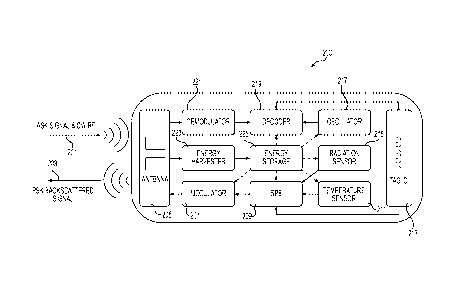
through which the RFID wireless dosimeter chip-enabled tags 101 through an
associated antenna
102 can communicate with a dosimeter reader 117. An amplitude-shift keying
(ASK) signal
(Tag ID 2.45 GHz RF signal) 111 is transmitted from the dosimeter reader 117
though an
antenna 119. The signal transmitted from the dosimeter reader 117, such as a
modulated radio
frequency signal, contains the predetermined ID corresponding to the wireless
dosimeter chip-
enabled tag 101 associated with the predetermined ID. After receipt of the
signal 111 from the
dosimeter reader 117 received by the corresponding antenna 102, a back
scattered signal 109
from the corresponding wireless dosimeter chip-enabled tag 101 associated with
the
predetermined ID containing the information from the respective wireless
dosimeter chip-
enabled tag 101 is transmitted by the respective antenna 102 and received by
the antenna 119 of
the dosimeter reader 117. The received back scattered signal 109 containing
the information or
data corresponding to a specific blood bag 105 is read by the dosimeter reader
117.
Date Recue/Date Received 2020-09-16
[0071] The dosimeter reader 117 is placed at a suitable distance from
the irradiation
apparatus 113, as can depend on the use or application, such as typically at a
maximum distance
of up to 1 meter (m), from the irradiation apparatus 113, to receive the
radiation dosage
measured by the wireless dosimeter chip-enabled tags 101 associated with the
specific blood
bags 105 having the respective predetermined ID values. The dosimeter reader
117 can store or
can read out, such as wirelessly through the antenna 119 or through a wired
connection, the
information or data in the respective received backscatter signals 109 from
the corresponding
wireless dosimeter chip-enabled tags 101, such as the measured radiation dose
respectively
applied to blood in the specific blood bags 105, or other applicable data for
the blood in the
specific blood bag 105, such as the temperature of the blood irradiated, time
of irradiation or
other applicable information or data, for example.
[0072] The exemplary 2.45 GHz X-ray wireless dosimeter chip-enabled
tag 101 is
intended to replace or is a substitute for the aforementioned color indicator
RadTag labels. The
2.45 GHz wireless dosimeter chip-enabled tag 101 is typically used as a semi-
passive RFID tag
employing backscatter modulation and wireless power transfer to facilitate
minimal power
consumption and a low-form factor. The wireless dosimeter chip-enabled tag 101
associated
with embodiments of the antenna 102 desirably includes an energy harvesting
unit, such as a
rectifier and a capacitor-for self-powered operation.
[0073] Also, embodiments of the wireless dosimeter chip-enabled tag
101 include a
suitable wireless X-ray dosimeter chip-enabled tag sensor, such as embodiments
of a low-power
FG-MOSFET sensor in RF-CMOS technology, which sense the received radiation
dosage to the
blood bag 105, signal processing electronics, such as a suitable processor and
associated
memory, that convert measured data to pulses and a transmitter or modulator
that sends the
26
Date Recue/Date Received 2020-09-16
pulses through the antenna 102 to the dosimeter reader 117 operating in the
same frequency
band. Similar to the RadTag labels, the wireless dosimeter chip-enabled tags
are to be applied to
the blood bags 105 as schematically depicted in Fig. 1. The wireless dosimeter
chip-enabled tags
101 desirably are configured to communicate with the RF reader, such as the
dosimeter reader
117, typically at a maximum distance of one meter for blood irradiation
measurements, for
example. Also, it is desirable that power consumption of the wireless
dosimeter chip-enabled tag
101 is estimated to consume a power of 263 microwatts ( W) with a nominal
supply of 1.2 volts
(V), for example, although the power consumed can depend on the use or
application, and should
not be construed in a limiting sense.
[0074] Fig. 2 is a system-level diagram illustrating an embodiment of a
wireless
dosimeter chip-enabled tag 200 corresponding to the wireless dosimeter chip-
enabled tag 101 of
Fig. 1. The wireless dosimeter chip-enabled tag 200 has a predetermined ID
corresponding to
predetermined ID values of e-Fuses in a memory cell or fuse cell of a RFID tag
ID device 213
and includes other sub-modules of the wireless dosimeter chip-enabled tag 200.
The RFID tag
ID device is a necessary circuit block within the RFID tag in that is the
memory block which
can permanently keep a unique device ID for the wireless dosimeter chip-
enabled tag 200. The
system-level diagram of a RFID wireless dosimeter chip-enabled tag 200 and its
sub-modules,
as an exemplary embodiment of the wireless dosimeter chip-enabled tag 101, are
desirably
implemented in a 130 nanometer (nm) complementary metal oxide semiconductor
(CMOS)
process, for example, and desirably is integrally formed on an integrated
circuit chip, such as a
wireless electronic silicon-based dosimeter chip, for example. The dosimeter
of the RFID
wireless dosimeter chip-enabled tag 200 is realized in a semi-passive RFID
(radio frequency
27
Date Recue/Date Received 2020-09-16
identification) tag configuration employing backscatter and a wireless RF
energy harvesting
module for low-power operation and low-form factor.
[0075] The wireless dosimeter chip-enabled tag 200 is uniquely
identified by a
predetermined ID which is desirably hard-coded into the tag's integrated
circuit (IC) in the e-
Fuses in a memory cell or fuse cell of the RFID tag ID device 213. The
wireless dosimeter
chip-enabled tag 200 includes an antenna 205 to receive an ASK signal 201 and
to transmit a
PSK backscattered signal 203. The ASK signal 201, such as a constant wave
radio frequency
(CW RF) signal, is transmitted via the antenna 205 to a demodulator 221 to
demodulate the
received ASK signal 201 and is coupled with a decoder 219 to decode the
received ASK signal
201 and an oscillator 217 to generate signals for operation of the wireless
dosimeter chip-
enabled tag 200. The decoder 219 is in communication with the RFID tag ID
device 213, which
includes a unique or predetermined ID associated with the wireless dosimeter
chip-enabled tag
200, as described herein. The RFID tag ID device 213 is in communication with
a signal
processing engine (SPE) 209, or other suitable processor, including or
associated with a
memory for programs, instructions or data storage for operation and control of
the wireless
dosimeter chip-enabled tag 200, such for processing, transmitting or receiving
requests, data or
information in or by the wireless dosimeter chip-enabled tag 200. The SPE 209
is coupled to a
modulator 207 which modulates and formats an information or data signal, such
as the PSK
backscatter signal 203, for transmission from the antenna 205 to a receiver,
such as to the
dosimeter reader 117.
[0076] The wireless dosimeter chip-enabled tag 200 further desirably
includes a
temperature sensor 211 to sense the temperature of an object, fluid or other
medium associated
with the wireless dosimeter chip-enabled tag 200, such as blood in the blood
bag 105 being
28
Date Recue/Date Received 2020-09-16
irradiated, an energy harvester 223 which harvests the energy from the
received ASK signal 201
which is in communication with an energy storage module 225 to store the
energy from the
received ASK signal 201, which is in turn in communication with a low-power FG-
MOSFET
sensor in RF-CMOS technology radiation sensor 215 that senses an amount of
radiation
delivered to an object, such as blood in the blood bag 105. The components of
the wireless
dosimeter chip-enabled tag 200 are communicatively associated with each other
through the
SPE 209 to perform the functions and operations of the wireless dosimeter chip-
enabled tag
200, such as to determine an amount of radiation delivered to the blood bag
105. The wireless
dosimeter chip-enabled tag 200 can be modified to perform other applications,
as can utilize
similar components to those described and additional components for such other
applications,
for example. To communicate with a specific wireless dosimeter chip-enabled
tag 200, a reader,
such as the dosimeter reader 117, transmits the ASK signal 201, such as an
ultra-high frequency
(UHF) 2.45 GHz ASK-modulated signal 201, containing the unique or
predetermined ID of the
wireless dosimeter chip-enabled tag 200 it wishes to interrogate for data or
information, such as
the amount of radiation delivered to blood in a specific blood bag 105, for
example.
[0077] For example, each wireless dosimeter chip-enabled tag 200,
such as the wireless
dosimeter chip-enabled tag 101 inside the irradiation apparatus 113, such as
the Raycell Mk2
irradiator, demodulates the RF signal received through the antenna 205 and
compares the
received ID to its own unique or predetermined ID. If the IDs match, the
wireless dosimeter
.. chip-enabled tag 200 transmits its predetermined ID from the tag ID 213, a
sensed X-ray dose
from the radiation sensor 215, and measured temperature from the temperature
sensor 211
through the antenna 205 to a receiver, such as the dosimeter reader 117, using
backscatter
modulation. For example, the dosimeter reader 117 establishes a backscatter
link by
29
Date Recue/Date Received 2020-09-16
broadcasting a 2.45 GHz CW carrier tone as the ASK signal 201. During uplink
communication, the specified wireless dosimeter chip-enabled tag 200 modulates
its data, such
as radiation, temperature and the predetermined ID value, onto this CW carrier
signal using
PSK modulation, and reflects the signal as the PSK backscattered signal 203
back to the
dosimeter reader 117. Desirably, the interrogations of the wireless dosimeter
chip-enabled tag
200, and the transmission and reception communications are carried out using
the antenna 205
operating at 2.45 GHz, for example. Examples of a suitable antenna 205 are
described in
Sansui et al., "Development of a 2.45 GHz Antenna for Flexible Compact
Radiation Dosimeter
Tags", IEEE Transactions on Antennas and Propagation", April 16, 2019.
[0078] Fig. 3 shows a diagrammatic illustration of an embodiment of the
integrated
circuit chip 300 for the RFID tag ID device 213, such as for a wireless
radiation dosimeter or
other applications, according to the present invention. The overall memory
chip layout for the
integrated circuit chip 300, schematically shown in Fig. 3 includes all the
input, output and test
signal pads. The overall chip integrated circuit chip 300 measures at 1.5
millimeters (mm)x 1.5
mm including the bonding pads, which is then incorporated in a wireless
dosimeter chip-enabled
tag, such as the wireless dosimeter chip-enabled tag 200, for example.
[0079]
Fig. 4 shows a schematic block diagram of circuity and a schematic circuit
chip
layout for embodiments of a RFID tag ID device 400, corresponding to the RFID
tag ID device
213, such as for a wireless radiation dosimeter, according to the present
invention.
[0080] The RFID tag ID device 400 has two major roles within a blood bag
irradiation
dosimeter system. The first role relates to the necessity to be able to
identify a blood bag from
another blood bag by the unique bit pattern that each dosimeter tag memory
block has saved in it.
For example, in an irradiation apparatus, such as the irradiation apparatus
113, there can be
Date Recue/Date Received 2020-09-16
multiple blood bags close to each other with each blood bag having a tag
affixed on it and it is
desirable that each blood bag be required to be identified from each other
blood bag for tracking
purposes. The second role relates to the necessity to be able to initiate a
command to a specific
RFID tag to send the radiation data back to the reader for that specific RFID
tag. If there is no
specific identification for each of the RFID tags, once a read data command is
sent to the RFID
tags, it is likely all of the RFID tags would respond back at the same time
and that likely would
cause jamming or possible error in the reading back of the dosimetry data
measured or recorded
by the RFID tag, for example.
[0081] The RFID tag ID device 400 includes a plurality of inputs 401,
402, 403, 404 and
405, indicated in Fig. 4 for the write operation of the predetermined ID
values to e-Fuses 443 and
the read operation of reading the predetermined ID values of the e-Fuses 443
from the memory
cell or fuse cell 442 that provide the predetermined ID for the RFID tag, such
as the RFID tag
200, for example.
[0082] The RFID tag ID 400 device includes a reference/bias generator
410 that provides
reference currents and voltages as indicated Fig. 4 and Figs. 5A-5E, 7 and 9
that facilitate
minimizing or reducing fluctuations in the on-chip generated useful power
which can translate
into undesirable fluctuations in the VDD signal. Considering that the RFID tag
is designed for
wireless operation and powered wirelessly using an external source such as
power in a received
RF signal, such as from the ASK signal & CW RF 201 signal, fluctuations in the
on-chip
generated useful power can occur which can translate into fluctuations in the
VDD signal.
Fluctuations in the VDD signal can typically be detrimental to the correct
operation of the
memory block of the RFID tag ID device 400. The reference currents and
voltages provided by
the reference/bias generator 410 facilitate immunizing the read operation of
the e-Fuses 443 in
31
Date Recue/Date Received 2020-09-16
the memory cell or fuse cell 442 against unavoidable fluctuations. Any changes
in Vuu could
result in unpredictable changes mainly in incorrect memory cell reading. For
example, if the
actual bits which correspond to the predetermined ID values for the
predetermined ID are
011001101, then VDD fluctuations could mistakenly read such predetermined ID
values in the
memory cell or fuse cell as any random value, such as 01000101.
[0083] Fig. 5A shows a schematic block diagram of the circuity for an
embodiment of a
reference/bias generator 410 of Fig 4 for embodiments of a RFID tag ID device
400, according
to the present invention. The reference/bias generator 410 includes a start-up
component block
502 that receives the voltages indicated in Fig. 5A for generation of the
voltages and currents for
operation of the RFID tag ID device 400. The reference/bias generator 410 also
includes current
reference component block 504 that provides currents for operation of the RFID
tag ID device
400. Further, the reference/bias generator 410 includes a reference sense
component 508 circuit
that senses the presence of a set reference voltage used in comparing the e-
Fuse 443 state with
the set reference voltage in order to decide whether the e-Fuse 443 is at a
'0' or '1' state, for
example, the reference sense component 508 providing the reference voltage to
a reference
resistor 506.
[0084] Also included in Fig. 5A in the reference/bias generator 410
is the reference
resistor 506 that provides a reference resistance used in the determination of
whether a non-
charge based memory component is in a certain state, such as a first state or
a second state
indicating the predetermined ID value for a non-charge based memory component,
such as for
the e-Fuse 443 or other suitable non-charged based component, as can depend on
the use or
application, and should not be construed in a limiting sense. For example, for
an e-Fuse 443, if
the e-Fuse 443 is blown, in a non-conducting state, or if the e-Fuse 443 is
intact, in a conducting
32
Date Recue/Date Received 2020-09-16
state, such conducting or non-conducting state indicates a predetermined ID
value for the e-Fuse
443. The reference resistor 506 can provide a resistance to determine if the e-
Fuse 443 is intact,
and it provides a resistance to measure a resistance of around 50 ohms to 150
ohms which can be
interpreted as a digital '0' indicating the e-Fuse 443 is intact, and if it is
"burnt", such by passing
a one-time large current of 10-15 mA, then the fuse is broken and it reads a
higher resistance.
This higher resistance can be interpreted as a digital '1'. The reference/bias
generator 410 also
includes an isolating component, such as an isolating PMOS transistor 510.
Isolation of the low
voltage "reference/bias generation" block using the isolating PMOS transistor
510, such as a 100
gm wide MOSFET 'X' (See also Figs 7 and 9). Once a voltage VDDH = 3.3 V is
applied, the
PMOS 'X' turns off which isolates the "reference/bias generation" block from
the high voltage
3.3 V "FPOS" node. The 100 gm PMOS device acts to stop the high voltages
during a write
operation from breaking and damaging the circuit in the reference/bias
generator 410 block.
[0085] Continuing with reference to Fig. 5A, in order to minimize-
fluctuations of current
output with respect to VDD and also to facilitate that VREF and VFUSE do not
cross each other, a
current reference and bias generator circuit was provided as the
reference/bias generator 410. In
the reference/bias generator 410 of Fig. 5A, the MOSFETs T3, T7, T8, T6 and
resistor OPrpp8
create a current reference circuit for generation of a reference current. The
MOSFETs T35, T4,
and resistor OPppc0 create a startup circuit. The sizes of these components
are desirably
adjusted to reduce the current consumption in this part of the reference/bias
generator 410
circuit. The reference/bias generator 410 circuit block facilitates minimizing
fluctuations of
current output with respect to VDD and also facilitate ensuring that VREF and
VFUSE do not cross
each other. The choices made in the MOSFETs in the reference/bias generator
410 circuitry also
are such to facilitate minimizing the ionizing radiation effect on the circuit
components, such as
33
Date Recue/Date Received 2020-09-16
by desirably using regular "thin" oxide MOSFETs where needed and using "thick"
oxide
transistors elsewhere. The thick oxide MOSFETs are noted with "33" beside each
MOSFET in
Fig. 5A. In the reference/bias generator 410, regardless of the supply voltage
change VDD, the
voltages VREF and VFUSE are therefore able to desirably stay separated from
each other, as is
desirable for use in RF wireless dosimeter applications, for example.
[0086] As shown in Fig. 5A, the isolating PMOS 510 cuts off the 3.3 V
supply from the
low voltage side during programming of the e-Fuses 443 of the fuse cell or
memory cell 442.
For sensing (reading) of the e-Fuses 443, as VD/Hi is grounded, VDD is
connected through another
isolating component, an isolating PMOS transistor 407 (Fig. 5C) to the e-Fuses
443, the PMOS
transistor 407 being a programming transistor in the programming of the e-
Fuses 443. The size
of this isolating transistor, such as the isolating PMOS 407, is desirably
chosen to minimize the
voltage drop across its drain source. A transmission gate (i.e. an NMOS in
parallel with the
isolating PMOS 407) is not used in that the aim of the design of the
reference/bias generator 410
is to operate independent of a 3.3 V signal during the sensing or reading
operation which relies
on the on-chip generated voltage, such as is desirably utilized for wireless
dosimetry applications
of an RFID tag, for example.
[0087] For the read operation, the reference/bias generator 410
receives the VDD in the
range of 0.53 V to 1.2 V, for example, and outputs three signals. A first
signal VREF is used to
compare the e-Fuse 443 state with a set reference voltage in order to decide
whether the e-Fuse
.. 443 is at a '0' or '1' state. A second signal FPOS is provided to a system
memory component
block 440 of the RFID tag ID device 400 that includes the fuse cell or memory
cell 443 that
includes the e-Fuses 443, and the signal VFUSE is the fuse voltage coming out
of the system
memory component block 440. A third signal VimAs is provided that goes into a
read/write
34
Date Recue/Date Received 2020-09-16
component block 444 of the system memory component block 440 to enable the
reading
operation of the predetermined ID values of the e-Fuses 443. Also, the signal
VmAs goes
specifically to NMOS transistor B in the read/write component block 444 (Fig.
9) for the read
operation. Also, the signal FPOS is the line feeding the supply voltage and
the read current to
each of the 8 e-Fuses 443, and the signal FPOS voltage is desirably at VDD for
the read operation,
for example.
[0088] The RFID tag ID device 400 also includes a straight ring
counter 415 that
provides a plurality of ring signals, such as the ring signals Q1 to Q8, the
ring signals Q1 to Q8
respectively corresponding to each of the eight e-Fuses 443 for reading or
writing the
corresponding predetermined ID to the corresponding e-Fuse 443 for the
predetermined ID of the
RFID tag, such as the for the wireless dosimeter chip-enabled tag 200, for
example. The straight
ring counter 415 facilities an orderly and accurate writing of the bits, or
predetermined ID
values, for the e-Fuses 443, since it is not possible to write all the bits in
the e-Fuses 443, such as
8 bits corresponding to 8 e-Fuses in the memory cell or fuse cell 442, at the
same time. The
straight ring counter 415 is operated by the R CLK signal received by the gate
412, the R CLK
signal generating the ring signals Q1 to Q8.
[0089] The "R CLK" or "Read CLK" is desirably integrated onto the
RFID tag ID device
chip 400 or can be integrated into the wireless dosimeter chip-enabled tag
200, for example, such
as to provide clock signals for operation of the wireless dosimeter chip-
enabled tag 200. A
circuit block which can be implemented to perform the read clock task can be
in the form of a
ring oscillator which takes up a very small space on the chip and consumes an
ultra-low amount
of power compared to the rest of the circuit. The frequency of the read clock
can be in the range
of 10's of MHz, for example. The amplitude of the read clock signal is
desirably in the range of
Date Recue/Date Received 2020-09-16
0.53 V to 1.2 V. The lower the amplitude the slower the speed and also the
power consumption
would be lower. Also, for radiation sensing, the speed of the read clock does
not have to be so
high since radiation sensing does not require nanoseconds of resolution.
However the speed and
design of the read clock can depend on the use or application of the RFID tag
ID device 400, and
should not be construed in a limiting sense.
[0090] In relation to a desirable feature of the straight ring
counter 415 in the RFID tag
ID device 400, it is important to note that if in the worst case scenario, all
the bits of the e-Fuses
in the memory cell to be written are to be l's, as in 11111111, then that
means if these bits were
to be written in parallel, all the e-Fuses typically would receive 10-15 mA of
current
simultaneously, which can likely damage the chip and would also mean that the
transistors 'Y'
and 'W' (See Figs. 5A-5D, 7 and 9) would likely be unrealistically large which
would consume
space on chip for the RFID tag ID device 400 as would likely add to the cost
of the production.
However, by using the ring counter 415, the number of bits in the memory
design does not
change any design parameters, namely the size of the transistors 'Y' and 'W',
for example,
thereby facilitating the adaptability for expansion, such as in relation to
the memory cell and the
number of e-Fuses 443, for example.
[0091] The RFID tag ID device 400 also includes a gate 412 that
receives and provides
read and write clock signals in response to read/write enable signals as
indicated in Fig. 4 to the
straight ring counter 415 and to an 8 bit shift register 430 through a gate
424 for the reading and
writing operation of the e-Fuses 443 in the memory cell or fuse cell 442.
[0092] The RFID tag ID device 400 includes the system memory
component block 440
that includes the fuse cell or memory cell 442 that includes the e-Fuses 443.
The memory
system component block 440 also includes a read/write component block 444, an
output
36
Date Recue/Date Received 2020-09-16
select/isolation component block 448 and a write decision component block 446.
Embodiments
of components of the system memory component block 440 and their function and
operation are
further illustrated in Figs. 5A-5E, 7 and 9, for example.
[0093] Fig. 5D shows a schematic block diagram of an embodiment of
the circuity for
components of the memory system component block 440 of Fig. 4 for the output
select/isolation
component block 448 circuitry for embodiments of the RFID tag ID device 400,
according to the
present invention. Figure 5D illustrates the memory system component block 440
and the
circuity associated with controlling sensing, or reading, and programming of
the e-Fuses 443 of
the memory cell or fuse cell 442, and illustrates the programming current path
and signal
conditions for the sensing and programming operations, for example.
[0094] Fig. 5D illustrates signal values in the case of programming
an e-Fuse 443. Qi is
any data bit passed to the registers, such as an 8-bit shift register 430 of
the RFID tag device 400;
RingQi is the output of the straight ring counter 415 that starts up after the
first 8 clock cycles.
The counter's "1" output rotates through the e-Fuse cells 443 one at a time.
In other words, the
e-Fuses 443 can only be written in series due to a large amount of current
needed to program a
fuse. The size of the program NMOS has been determined in order to pass a
large current and
the routing metals connecting this MOSFET to the e-Fuse 443 and to the supply
(3.3 V) and to
ground have also been sized as per layout rules in order to avoid any electro-
migration or ground
lifting, or voltage drop along them. The signal COF is the program enable
signal which is set
.. "High = 3.3V" for programming and "Low = 0 V" for sensing. As illustrated
in Fig. 5D, another
isolation component, such as an isolating PMOS 409, is placed between the
output
select/isolation component block 448, a sense/program circuit block, and the
VFusE output to a
clocked comparator 420 of the RFID tag ID device 400 to protect the clocked
comparator 420's
37
Date Recue/Date Received 2020-09-16
input from the high voltages resulting from the programming step of
programming the e-Fuses
443. The transmission gate only turns ON to sense the e-Fuses 443 one at a
time. The VFusE
line is shared among the e-Fuses 443 and the e-Fuses 443 need to be isolated
from that line and
only one value is loaded onto the line at a time.
[0095] As mentioned, the RFID tag ID device 400 of Fig. 4 includes the
clocked
comparator 420 that communicates signals with a gate 422 that provides the
signals of the RFID
tag ID device 400, as indicated in Figs 4 and 5B, to the 8 bit shift register
430 for the reading and
writing operation of the e-Fuses 443 in the memory cell or fuse cell 442.
Also, read and write
clock signals and signals for the read and write operations, as indicated in
Figs 4, 5B and 5E, in
response to read/written enable signals as indicated in Fig. 4 are provided to
and from the
clocked comparator 420 to the gate 424 and signals are provided to and from
the gates 422 and
424 to the 8 bit shift register 430 for the reading and writing operations of
the e-Fuses 443 in the
memory cell or fuse cell 442. The shift register 430 provides the ring signals
Q1 to Q8 for
individually and respectively writing and reading the predetermined ID values
for the
predetermined ID of a RFID tag, such as the wireless dosimeter chip-enabled
tag 200, for
example.
[0096] Fig. 5B shows a schematic block diagram of the circuity for an
embodiment of a
clocked comparator 420 and shift register 430 of the RFID tag ID device 400 in
communication
with gates 422 and 424 circuitry of the RFID tag ID device 400 of Fig. 4 for
reading in a bit data
pattern to the registers to be written to the e-Fuses 443 of the fuse cell or
memory cell 442 for
embodiments of the a RFID tag ID device 400, according to the present
invention. Programming
an e-Fuse within this technology requires a ¨3.3 V supply and ¨10-15 mA of DC
current for a
duration of > 200 microseconds ( s). Fig. 5B shows the first 8 clock cycles
that pushes the 8 bit
38
Date Recue/Date Received 2020-09-16
data pattern to the registers before being written in the next 8 clock cycles
and illustrates the
reading in the 8 bit data pattern to the registers of the shift register 430
to be written to the e-
Fuses 443. Fig. 5B further indicates in more detail the circuitry and signals
to and from the
clocked comparator 420, the gates 422 and 424 and to and from the shift
register 430 in response
to read/written enable signals for the reading and writing operations of the e-
Fuses 443 in the
memory cell or fuse cell 442.
[0097] Fig. 5E shows a schematic block diagram in further detail of
an embodiment of
the clocked strong arm latch comparator 420 and the gates 422 and 424 and the
circuitry and
signals to and from the clocked comparator 420 and the gates 422 and 424 for
sensing the
predetermined ID values of the e-Fuses 443 of the fuse cell or memory cell 442
in reading out
the predetermined ID values for the corresponding e-Fuses 443 for embodiments
of a RFID tag
ID device 400, according to the present invention. Fig. 5F shows a schematic
block diagram of
circuity and a schematic circuit chip layout for an embodiment of the clocked
comparator 420 of
Figs. 4, 5B and 5E for embodiments of a RFID tag ID device 400, according to
the present
invention.
[0098] The read/write component block 444 receives the ring signals
Q1 to Q8 from the
straight ring counter 415 and the read current and write current from the
reference/bias generator
410 to provide for reading and writing the predetermined ID values to and from
the e-Fuses 443
corresponding to the predetermined ID of the RFID tag, such as the RFID
wireless dosimeter
chip-enabled tag 200. The read/write component block 444 receives the voltage
VmAs from the
reference/bias generator 410 to provide to an output select/isolation
component block 448 of the
system memory component block 440. The output select/isolation component block
448
receives the ring signals Q1 to Q8 along with the voltage generated (VFusE
INT) from the
39
Date Recue/Date Received 2020-09-16
read/write component block 444 provided from the voltage VBIAS to enable the
reading of each e-
Fuse 443 of the memory cell or fuse cell 442. Then the voltage generated
(VFusE INT) gets
transferred through the output select/isolation component block 448 which
creates VFUSE. In
each read clock cycle, the voltage of one of the e-Fuses 443 (bits) is
reflected on the VFUSE line
which gets compared to the VREF through the clocked comparator 420 of the RFID
tag ID device
400, and a signal is generated (Fuse Read, Fig. 5B), which is saved in the
registers of the 8-bit
shift register 430 of the RFID tag ID device 400.
[0099] Continuing with reference to Figs. 4 and 5C, an embodiment of
an e-Fuse
programming system block including read/write control circuit blocks including
the write
decision component block 446 and the fuse cell or memory cell 442 are
illustrated of the memory
system component block 440 of the RFID tag ID device 400, with Fig. 5C showing
in more
detail a schematic block diagram of an embodiment of the circuity for an e-
Fuse programming
system block components of Fig. 4. The write decision component block 446
("Fuse Write
Input" block) receives and provides the signals indicated in Figs. 4 and 5C
for the write
operation to write the predetermined ID values to the e-Fuses 443 of the fuse
cell or system
memory 442.
[00100] Continuing with reference to Figs. 4 and 5C, in the operation
of the read/write
control circuit blocks including the write decision component block 446 in
writing the
predetermined ID values to the e-Fuses 443 of the fuse cell or memory cell
442, the three signals
Qi, RingQi, and COF need to be "High" in order for the level shifter inside
the write decision
component block 446 ("Fuse Write Input" block) to output a "High = 3.3 V"
signal to enable a
programming NMOS transistor 407 to provide the programming current. Then the
programming
current flows as shown in Figs. 5C and Fig. 5D, for example.
Date Recue/Date Received 2020-09-16
[00101] An "un-burnt" e-Fuse measures ¨50 S2 to 150 S2 and a burnt one
measures
¨4,000 a Therefore, the e-fuse memory cell 442 requires a write circuitry that
burns each e-
Fuse 443 by applying a high-voltage (-3.3 V) and a large current (-10-15 mA)
for
programming the e-Fuses 443 and also a low power sense circuitry, such as for
the read/write
component block 446, that reads the bit string produced by the combination of
burnt and unburnt
e-Fuses 443 (Fig. 9). The application of 3.3 V to each e-Fuse 443 cell
requires the use of the
high-voltage (3.3 V) variation of transistors for the write stage since,
standard transistors, as
typically used, cannot withstand such high voltages, for example. Also, during
the read
operation of the e-Fuses 443 of the fuse cell or memory cell 442, the write
decision component
block 446 is completely off, such as indicated in Fig. 9.
[00102] Fig. 6 shows a table 600 illustrating exemplary input signals
from read and write
operations for the non-volatile memory (NVM) e-Fuses 443 of the fuse cell or
memory cell 442
for embodiments of the RFID tag ID device 400 circuitry of Fig. 4, associated
with writing into
the NVM memory and reading from the NVM memory the predetermined ID values
corresponding to a predetermined ID of a RFID tag, according to the present
invention.
[00103] The overall read/write operations in reading and writing of
the RFID tag
predetermined ID to the e-Fuses 443 of the memory cell or fuse cell 442 of the
RFID tag ID
device 400 desirably requires 8 input signals @ads) and 2 supply pads for VDD
and ground, such
as generally illustrated in the integrated circuit chip 300 for the RFID tag
ID device, with the
input signals being indicated in Figs. 4, 5A-5E, 7 and 9, for example. Table
600 shows the input
signals for the read and write operations of the e-Fuses 443 of the memory
cell or fuse cell 442
of the RFID tag ID device 400.
41
Date Recue/Date Received 2020-09-16
[00104] Referring to table 600, the Reset signal is used to clear any
possible bit values
from the registers of the 8-bit shift register 430 and also is a necessary
signal in conjunction with
Pulse in signal to start the straight ring counter 415. The Read clk signal is
used for reading out
of the memory bit pattern of the predetermined ID values of the e-Fuses 443
from the memory
cell or fuse cell 442. The Read clk signal is to be generated on chip through
the use of a ring
oscillator of the straight ring counter 415 or any other clock generator
block. The operating
voltage of the Read clk signal desirably matches the read operation supply
range of 0.53 V to
1.2V for example. Through the use of a phase shifter 423 (Fig. 9) and a
frequency divider the
Read clk signal is divided and two signals are generated which are the Comp
clk (Comparator
CLK) signal and the SR clk signal. The Comp clk signal is the comparator clock
for the
comparator 420 and the Comp clk signal arrives earlier than the SR clk signal.
The Comp clk
signal pre-charges the nodes to VDD on the falling edge as shown in Figure 5E.
On the rising
edge of this clock, the evaluation period starts where a decision is made
based on the input
values to the differential pair, for example.
[00105] Continuing with reference to table 600, The Pulse in signal has the
task of starting
the straight ring counter 415, which carries a logical "1" through the eight
(8) ring signals to the
read/write component block 444, in the starting of the writing of the
predetermined ID values to
the e-Fuses 443; and the outputs of the straight ring counter 415 are
identified as the signals
RingQi, RQi, RQib. The Write clk signal is applied to a separate pad of the
RFID tag ID device
400, such as can be externally applied to the RFID tag ID device 400 or can be
applied internally
from the wireless dosimeter chip-enabled tag 200 when the RFID tag ID device
400 is integrated
with the wireless dosimeter chip-enabled tag 200, for example, to perform the
writing task of
writing the predetermined ID values to the e-Fuses 443. The clock amplitude
for the writing
42
Date Recue/Date Received 2020-09-16
operation is set to VDD of 1.2 V and not to 3.3 V, for example. The Write clk
signal is grounded
for the reading operation of the e-Fuses 443 of the fuse cell or memory cell
442.
[00106] Further, with reference to the table 600, the Data Write
Enable signal is a constant
"1" and is used only during the writing operation of writing the predetermined
ID values to the e-
Fuses 443. The Data Write Enable signal acts on the multiplexers (MUX's) of
the RFID tag ID
device 400 used to carry out the write or read tasks in reading from or
writing to the e-Fuses 443
the predetermined ID values. The Data signal is an 8 bit pattern passed to the
registers of the 8-
bit shift register 430 serially before the writing operation of writing to the
e-Fuses 443 the
predetermined ID values. The C OF signal enables or disables the access to the
VDDH supply
voltage. The C OF signal is also necessary for enabling the write operation on
each individual
e-Fuse 443. The VD/Hi signal is set at 3.3 V for the writing operation only
for writing to the e-
Fuses 443 the predetermined ID values. The VDDH signal also isolates through
the isolating
component PMOS 510, the MOSFET T2, shown in Figure 5A, the standard MOSFETs in
the
reference current source in the current reference component block 504 from
possible damage.
The VD/Hi signal also isolates the input VFuse of the clocked comparator 420
and any possible
current path from the fuse cell block 442 shown in Figure 5D during the
writing operation for
writing to the e-Fuses 443 the predetermined ID values. The GND signal is set
to 0 for the read
operation and the write operation of reading and writing the predetermined ID
values to the e-
Fuses 443, for example.
[00107] Fig. 7 shows a schematic block diagram of circuity and a schematic
circuit chip
layout for embodiments of a RFID tag ID device 400 of Fig. 4 illustrating the
write operation of
writing the predetermined ID values to the e-Fuses 443 showing circuitry
associated with and
embodiments of methods for the write operation for the non-volatile memory
(NVM) e-Fuses
43
Date Recue/Date Received 2020-09-16
443 of the fuse cell or memory cell 442 for writing into the NVM memory the
predetermined ID
values corresponding to a RFID tag ID, according to the present invention.
[00108] Continuing with reference to Fig. 7, as well as to FIG. 4 and
5A-5E, an
embodiment of the method for the write operation for writing the predetermined
ID values to the
.. e-Fuses 443 and components of the RFID tag ID device 400 involved in the
write operation are
described. The write operation involves circuitry and components of the RFID
tag ID device 400
including the reference/bias generator 410, the ring counter 415, the
read/write component block
444, the write decision component block 446, the output select/isolation block
448, the gates 422
and 424 and the 8 bit shift register 430, the function and operation of these
components of the
RFID tag ID 400 in relation to the write operation of the e-Fuses 443 are
indicated in Fig. 7, for
example.
[00109] Continuing with reference to Figs. 4 and 7, in the write
operation of Fig. 7, an
external pad inputting an external clock signal with an amplitude of 1.2 V
with a possible signal
period of 400 i.is was used in application of a clock signal to the RFID tag
ID device 400. A
.. faster clock signal might result in shorter writing time, but such faster
clock signal, might not
completely burn an e-Fuse 443 in writing the predetermined ID value to the e-
Fuse 443. A
longer clock time could be used, and a clock period value above 400 s can be
used to write the
predetermined ID values to the non-charge-based memory components, the e-Fuses
443, of the
memory cell or fuse cell 442, as can depend on the use, configuration or
application of or for the
RFID tag ID device 400, and should not be construed in a limiting sense. A
voltage for VDDH =
3.3 V is applied to the RFID tag ID device 400 in various places for the write
operation as
indicated and shown in Figure 7, for example.
44
Date Recue/Date Received 2020-09-16
[00110] In the output select/isolation block 448, the PMOS transistor
'Z' gets 3.3 V during
the write operation. The PMOS transistor "Z" functions as further isolating
component to isolate
the high writing voltage from getting to the low-voltage circuitry in the
clocked comparator 420.
Also, the output select/isolation block 448 desirably includes a PMOS/NMOS
combination 'A'
for the writing and reading operation. As can be seen from Figs. 4 and 7, the
Write CLK (W
CLK) signal runs the 8-bit shift register 430 and the straight ring counter
415. The first 8 clock
cycles are used to feed 8 bits of data (comprised of O's and l's) to the 8-bit
shift register 430
while through the use of the "C OF" signal, the rest of the RFID tag ID device
400 circuit
components are not operating for this part of the write operation. After the
first 8 clock cycles,
the 8-bit shift register 430 is full with the data bits to be written into the
e-Fuses as the
predetermined ID values for the predetermined ID. They are located at each of
the Q1 to Q8
signal lines from the 8-bit shift register 430. Then the next 8 clock cycles
are used to write each
value of Q1 to Q8 onto the e-Fuses 443.
[00111] In the write operation, the ring counter 415 sequentially
creates a '1' value within
"RingQ1" to "RingQ8" for the corresponding predetermined ID value, while the
rest of the
"Ring Ql" to "Ring Q8" signal values are O's.
[00112] For example, the RingQ's created by the ring counter 415 work
as
follows:1000000040100000040010000040001000040000100040000010040000001040
0000001.
[00113] Continuing with reference to Figs. 4 and 7 for the write operation,
the C OF
signal changes value to VDD at the beginning of the 9t1i clock cycle and the
data in each ring
signal Q1 to Q8 are sent to the write decision component block 446 shown in
Figs. 4 and 7. The
three signals of RingQ, Q, and C OF are then together combined with an "AND"
operation and
Date Recue/Date Received 2020-09-16
if all of them are '1', then a "Write Fuse" command shown in Fig. 4 is applied
to the NMOS in
the read/write component block 444 in Fig. 7 which then lets a current, such
as in a range of 10
mA to 15 mA flow through the 1st e-Fuse 443 through the PMOS transistor 'Y' in
Fig. 7. During
the write operation, the MOSFETs in 'A', 'X' and 'Z' in Fig. 7 stop any high
voltages of
approximately 3.3 V to get to other parts of the RFID tag ID device 400
circuit which can get
damaged by such voltage applied during the write operation.
[00114] The write operation of Fig. 7 then continues for the 2nd e-
Fuse 443, again the Ring
Q2 signal is chosen with Q2 and the C OF signal, and if the AND operation
result is '0', nothing
happens to the e-Fuse 443, such that the 2nd e-Fuse 443 remains intact, having
the corresponding
predetermined ID value for an intact e-Fuse 443, and no current flows through
PMOS 'Y' of Fig.
7. The write operation, as described herein, then continues sequentially for
the 3' through the 8'
e-Fuses. After 8 cycles of the write operation for writing the predetermined
ID values to the
eight e-Fuses 443 for the predetermined ID, the RingQ signal has reached it
last bit shown above
(00000001) for the ring signal Q8 and, as such for an 8-bit memory, no more
bits are left to be
written to the e-Fuses 443, therefore, the write session or write operation
has been completed for
the e-Fuses 443 of the fuse cell or memory cell 442 providing the
predetermined ID values for
the predetermined ID that uniquely identifies the RFID tag. Also, the above
write operation can
be performed for any number of e-Fuses or bits as may be needed for the
predetermined ID, as
can depend on the use, configuration or application for the RFID tag ID device
400, and should
not be construed in a limiting sense. In the write mode or write operation,
the value of the VDD
signal which operates all the logic components, such as the 8-bit shift
register 430, the ring
counter 415, and other component blocks of the RFID tag ID device 400 is
desirably set to 1.2 V,
for example.
46
Date Recue/Date Received 2020-09-16
[00115] Fig. 8 is a graphic illustration 800 of a fuse writing
operation sample signals
plotted as voltage (V) versus time T in microseconds (.1s) in embodiments of
methods for a write
operation to write predetermined ID values into the non-volatile memory (NVM)
e-Fuses 443 of
the fuse cell or memory cell 442 for embodiments of a RFID tag ID device 400
of Fig. 4 for a
corresponding to a RFID tag, according to the present invention. The graphic
illustration 800 of
Fig. 8 demonstrates a sample write operation signal pattern for the RFID tag
ID device 400 for
the write operation as described in relation to Fig. 7. It can be seen from
the graphic illustration
800 of Fig. 8 that 4 bits out of 8 bits for the e-Fuses 443 are being burnt by
applying 3.3 V which
allows a current of approximately z 18.5 mA to pass through the e-Fuses one at
a time in the
sample write operation for writing the predetermined ID values to the
exemplary eight e-Fuses
443 of the memory cell or fuse cell 442 corresponding to a predetermined ID
for a RFID tag, for
example.
[00116] Fig. 9 shows a schematic block diagram of circuity and a
schematic circuit chip
layout for embodiments of a RFID tag ID device 400 of Fig. 4 illustrating
circuitry associated
.. with and embodiments of methods for the read operation of reading the
predetermined ID values
from the e-Fuses 443 showing circuitry associated with and embodiments of
methods for the
read operation for the non-volatile memory (NVM) e-Fuses 443 of the fuse cell
or memory cell
442 for reading from the NVM memory the predetermined ID values corresponding
to a RFID
tag ID, according to the present invention.
[00117] Continuing with reference to Fig. 9, as well as to FIG. 4 and 5A-
5E, an
embodiment of the method for the read operation for reading the predetermined
ID values from
the e-Fuses 443 and components of the RFID tag ID device 400 involved in the
read operation
are described. The read operation involves circuitry and components of the
RFID tag ID device
47
Date Recue/Date Received 2020-09-16
400 including the reference/bias generator 410, the ring counter 415, the
read/write component
block 444 the write decision component block 446, the output select/isolation
block 448, the
gates 422 and 424, the 90 degree (900) read clock phase shifter 423, and the 8
bit shift register
430, the function and operation of these components of the RFID tag ID 400 in
relation to the
.. read operation of the e-Fuses 443 are indicated in Fig. 9, for example.
[00118] Continuing with reference to Figs. 4 and 9, as well as with
reference to Figs. 5A,
5C and 5E, the sensing operation or reading operation of the predetermined ID
values of the e-
Fuses 443 from the memory cell or fuse cell 442, involves the circuit blocks
shown in Figs. 5A,
5C, and 5E in addition to a clock input such as provided through the gates
412, 422 and 424, the
90 degree (90 ) read clock phase shifter 423, and the output shift registers
of the 8-bit shift
register 430. Instead of relying on pre-charging the bit line directly
connected to the e-Fuses
443, such as through access transistors, the read operation circuit topology
of the RFID tag ID
device 400 desirably pre-charges only the diffusion capacitances on nodes "X",
"Y", "AA" and
"BB", as indicated in Fig. 5E for the clocked comparator 420, prior to the
sensing or reading
operation of the predetermined ID values of the e-Fuses 443.
[00119] Also, another desirable benefit of the reading operation
circuit topology for the
clocked comparator 420, such as indicated in Fig. 5E, is that a relatively
better or best switching
(latching) performance can be achieved by using minimum size transistors. In
such circuit
topology, the pre-charger does not have to drive a large capacitor resulting
from many metal
routings connecting the e-Fuse nodes in parallel. Other benefits of using the
circuit topology of
Fig. 5E for the clocked comparator 420 are facilitating consuming zero static
power and directly
producing rail-to-rail outputs, for example. Since this circuit topology
relies on a voltage gain
resulting from the flow of charge from CAA and CBB, the input offset must be a
minimum offset
48
Date Recue/Date Received 2020-09-16
in order to increase the read sensitivity (i.e. the minimum input voltage
difference detectable).
Such desirable circuit topology for the clocked comparator 420, such as a
clocked strong arm
latch comparator, desirably can be implemented on a relatively symmetric
integrated circuit
layout for the clock comparator 420, such as illustrated in Fig. 5F, for
example.
[00120] Various considerations were taken into account in the desirability
of the sensing
topology of the RFID tag ID device 400 for the reading or sensing topology for
the read
operation of the e-Fuses 443. It was determined that a few resistors used in
the current reference
circuit block 504 of the reference/bias generator 410 and in the e-Fuse
reference resistor 506
desirably are of high or relatively high accuracy type. Such high accuracy
poly-resistors
typically have a smaller process variation but also occupy a much larger
footprint than low
accuracy poly-resistors.
[00121] In choosing the value of the reference resistor 506, as per
the technology
documentations, a typical eFuse would have a resistance 2:5 kiloohms (kS2).
Therefore, the
reference resistor 506 was desirably set at 2.5 kS2, the approximate midpoint
between 150 ohms
(S2) and 5 kS2, for example. Monte Carlo simulations were performed to
determine the trip point,
or the closet value, to the reference resistor 506, correctly detectable.
Also, a relatively
conservative design was considered for the reference resistor 506 in relation
to power
consumption. Typically, the lower the reference resistor value, the higher the
bias current
running through the reference resistor, such as the reference resistor 506 and
the e-Fuses, such as
the e-Fuses 443. While it is possible to assume a higher programmed e-Fuse
resistance, it is
desirable to provide for an e-Fuse resistance that facilitates a robust and
reliable operation, as
well as facilitates minimizing the footprint and power consumption for the
RFID tag ID device
49
Date Recue/Date Received 2020-09-16
400, for example, particularly as to the desirability of low-power wireless
operation of a RFID
tag for wireless dosimeter measurements, for example.
[00122] Continuing with reference to Figs. 4 and 9, as well as with
reference to Figs. 5A,
5C and 5E, the read operation of reading the predetermined ID values of the e-
Fuses 443 is
described in more detail. For the "read" operation or "sense" operation,
desirably the signal
VDDH ¨ C OF = 0.0 V or just the common ground of the chip including the RFID
tag ID device
400. This facilitates ensuring that the PMOS 'Y' is "OFF" or blocked, the PMOS
'X' is "ON" or
conducting and the PMOS 'Z' is "ON" or conducting, as indicated in Fig. 9.
Also, the write
decision component block 446 is disabled and the NMOS 'W' is "OFF", as
indicated in Fig. 9.
.. Further, the Read CLK" or "R CLK" signal for the read operation is applied
from an external pad
as indicated in Figs. 4 and 9, or the Read CLK" or "R CLK" signal can be
applied internally
from the wireless dosimeter chip-enabled tag 200, for example, as well as the
"W CLK" or
"Write Clk" signal for the write operation is disabled, such as by being
grounded, since the "W
CLK" or "Write Clk" signal is not utilized for the read operation, as the
write operation, in the
case of e-Fuses, only happens during the programming of the e-Fuses 443, and
the predetermined
ID values are read, not written, during the reading operation, for example.
[00123] Also, in the read operation, the "R CLK" signal is sent to the
90 degree (90 ) read
clock phase shifter 423 which generates the comparator clock and the required
clock to the 8-bit
shift register 430 which holds the 8-bit e-Fuse 443 values to be sent at the
end of the read cycle.
The 90 degree (90 ) read clock phase shifter 423 desirably facilitates
creating a delay between
the clocked comparator 420 and the 8-bit shift register 430 so that the
clocked comparator 420
has enough time to compare the e-Fuse 443 voltage value to the VREF voltage
and then save the
corresponding e-Fuse 443 voltage value into the 8-bit shift register 430. If
the same clock was
Date Recue/Date Received 2020-09-16
used to perform both tasks, then the 8-bit shift register 430 would likely
save a random (wrong
bit value) and, hence, an error would likely occur in the read operation of
the e-Fuses 443.
[00124] During the read operation, the write decision component block
446 is completely
off. For the first 8 read clock cycles, the 8-bit shift register 430 is
filling up with e-Fuse 443
values, and for the next 8 cycles, the e-Fuse 443 values can be collected from
the Q8 signal
output, such as from a Q8 signal output pad, from the shift register 430, such
as in a series read
operation, for example. Also, if all 8 bits corresponding to the signals Q1 to
Q8 are monitored,
the memory value can be read in a parallel format from corresponding Q1 to Q8
signal outputs,
such as from the corresponding Q1 to Q8 signal output pads, of the shift
register 430 after the
.. first 8 clock cycles for the parallel operation, for example. The
embodiment of the circuit of the
comparator 430 shown in Fig. 5E is desirably symmetrically laid out in an
integrated circuit chip,
as indicated and illustrated in Fig. 5F, in view of relatively high
sensitivity requirements, such as
for a relatively low-power RFID tag for wireless dosimeter applications, for
example.
[00125] Fig. 10 is a graphic illustration of a fuse read operation
signal flow for reading the
predetermined ID values of the e-Fuses 443 plotted as voltage in volts (V)
versus time T in
microseconds (.1s) in embodiments of methods for a read operation, as
described in relation to
Figs. 4, Figs. 5A, 5C and 5E and 9, the read operation to read the
predetermined ID values of a
predetermined ID of a RFID tag from the non-volatile memory (NVM) e-Fuses 443
of the fuse
cell or memory cell 442 for embodiments of a RFID tag ID device 400 of Fig. 4,
according to the
present invention.
[00126] Continuing with reference to Fig. 10, there is illustrated a
graphic illustration
1000 of an embodiment for a logical signal flow for a read operation of the
predetermined ID
values stored in the memory cell or fuse cell 442 of the RFID tag ID device
400. As illustrated
51
Date Recue/Date Received 2020-09-16
from Fig. 10, with reference to Figs. 4, Figs. 5A, 5C and 5E and 9, as the
Comp clk signal goes
HIGH, the pre-charging PMOS's of the reference/bias generator 410 turn off and
the evaluation
period begins by turning on the NMOS as shown in clocked strong arm latch
comparator 420
indicated in Fig. 5E. The two signals being compared are at the inputs of the
differential pair of
signals VREF and VFUSE, and the signals VREF and VFUSE. are set up, as
indicated from Fig.10, to
facilitate a relatively stable signal read operation of the predetermined ID
values of the e-Fuses
443.
[00127] In the read operation of Fig. 10, as the read clk signal
rises, the Comp clk signal
rises and, since the voltage value of VFUSE is lower than that of VREF, there
is no transition in the
Fuse Read signal. As the first SR clk signal positive signal edge arrives, it
passes the "1" to the
first register Qlout of the shift register 430. This process during the RingQ1
signal enables a
first e-Fuse 443 to be read. If VFUSE is less than < VREF, then the e-Fuse 443
has been blown (high
resistance) which is interpreted as a logical "1", otherwise if the e-Fuse 443
has not been blown
(intact) it is a logical "0" that provides the corresponding predetermined ID
value for the
corresponding e-Fuse 443.
[00128] The above read operation continues for the remaining e-Fuses
443 in the fuse cell
or memory cell 442 by repeating the above described operation for the other
RingQ signals,
RingQ2 to Ring Q8, for each of the remaining second through eighth e-Fuses
443. As the next e-
Fuse 443 is read, the ring Q signal for the previously read e-Fuse 443 goes
low and the next to be
read e-Fuse 443 ring Q signal goes high, such as the RingQ1 signal going low
and the RingQ2
signal going high for reading a second e-Fuse 443. If the voltage value VFUSE
is less than < VREF
for the e-Fuse 443 being read, then the e-Fuse 443 has been blown (high
resistance) which is
interpreted as a logical "1", otherwise if the e-Fuse 443 has not been blown
(intact) it is a logical
52
Date Recue/Date Received 2020-09-16
"0" for the e-Fuse 443 being read, thereby providing the corresponding
predetermined ID value
for the corresponding e-Fuse. The reading operation continues as described
until all values of
the e-Fuses 443 are determined that provide the corresponding predetermined ID
for the RFID
tag ID device associated with a RFID tag.
[00129] Also, it is noted that as the supply voltage is reduced from the
nominal 1.2 V to
0.53 V for the RFID tad ID device 400, the difference in voltage between VFUSE
and VREF reduces
to the point where reliable read operations are not likely. For the read
operation, the current
source circuit of the current reference component block 504 shown in Fig. 5A
advantageously
facilitates maintaining a difference between the two signal voltages VFUSE and
VREF within the
supply range to facilitate a reliable read operation of the predetermined ID
values of the e-Fuses
443, for example.
[00130] Referring now to Figs. 11-14, Fig. 11 is a graphic
illustration 1100 of direct
current (DC) current flow through the current source reference component block
504 of the
reference/bias generator 410 for embodiments of a RFID tag ID device 400 of
Fig. 4 indicating
the current in microamperes ( A) versus the voltage VDD (V) for reading the
predetermined ID
value of a low resistance, i.e., connected, e-Fuse 443 of the fuse cell or
memory cell 442,
according to the present invention. Fig. 12 is a graphic illustration 1200 of
direct current (DC)
current flow through the current source reference component block 504 of the
reference/bias
generator 410 for embodiments of a RFID tag ID device 400 of Fig. 4 indicating
the VDD current
draw in microamperes ( A) versus the voltage VDD (V) for reading the
predetermined ID value
of a high resistance, i.e., blown or not connected, e-Fuse 443 of the fuse
cell or memory cell 442,
according to the present invention.
53
Date Recue/Date Received 2020-09-16
[00131] Continuing with reference to Figs. 13 and 14, Fig. 13 is a
graphic illustration 1300
of direct current (DC) voltage values of VREF, VFUSE, and VBIAS for
embodiments of a RFID tag
ID device 400 of Fig. 4 indicating the voltage (V) versus the voltage Vp (V)
for a low resistance,
i.e., connected, e-Fuse 443 of the fuse cell or memory cell 442 as per VDD
sweep, according to
the present invention. Fig. 14 is a graphic illustration 1400 of direct
current (DC) voltage values
of VREF, VFUSE, and VmAs for embodiments of a RFID tag ID device 400 of Fig. 4
indicating the
voltage in millivolts (mV) versus the voltage VDD (V) for of a high
resistance, i.e., blown or not
connected, e-Fuse 443 of the fuse cell or memory cell 442 as per VDD sweep,
according to the
present invention.
[00132] The information in the graphic illustrations 1100, 1200, 1300 and
1400 of Figs.
11-14 are a result of the read operation described in relation to Figs. 4,
Figs. 5A, 5C and 5E and
9. A significant observation indicated from the graphic illustrations 1100,
1200, 1300 and 1400
is that regardless of the supply voltage change VDD, the voltages VREF and
VFUSE stay separated
from each other, as is desirable for the read operation of the e-Fuses 443, as
described.
[00133] Also, the graphic illustrations 1100, 1200, 1300 and 1400 of Figs.
11-14 were
derived from post-layout simulations since real device measurements would
require access to
internal nodes on chip for the RFID tag ID device 400. However, any results,
such as voltage or
current measurements described, other than the above mentioned simulations
were based on real
device measurements for the RFID tag ID device 400 and match the simulation
results.
Consequently, the simulation results for the graphic illustrations 1100, 1200,
1300 and 1400 of
Figs. 11-14 can also be considered as device measurement values for the RFID
tag ID device
400, for example.
54
Date Recue/Date Received 2020-09-16
[00134] As described, individual transistors' DC current values for
the RFID tag ID
device 400 are shown in Fig. 11 for the case of a "connected" e-Fuse 443 and
those for a
"blown" e-Fuse 443 are shown in Figure 12. Figs. 13 and 14 illustrate the
difference between
VREF and VFUSE as the supply voltage changes for a connected e-Fuse 443 and a
blown e-Fuse
443, respectively. As can be seen, except for the 160.3206 A curve and the
148.015 A curve
of Fig. 11 and the 144.310 A curve and the 130.6935 A curve of Fig. 12 all
the other currents
in Figs. 11 and 12 are substantially unchanged throughout the range of supply
voltages for the
RFID tag ID device 400. The -184.118 A curve in Fig. 11 and the -174.765 A
curve in Fig.
12 illustrate the entire chip's current draw for the RFID tag ID device 400.
The transistors'
currents in Fig. 11 correspond with the transistors in reference/bias
generator 410 of Fig. 4
illustrated in more detail in Fig. 5A.
[00135] As illustrated from Figs. 11 and 12, the current curves for
the "T2" and "T10"
transistors of the reference/bias generator 410 of Fig. 4 and Fig. 5A are not
constant with supply
voltage. The transistor "T10"s gate is biased internally which would make it
draw current
independent of the supply much like other transistors in the circuit and,
therefore, instead of
using a PMOS transistor at a location of the reference resistor 506, the
reference resistor 506 is
used instead, as illustrated in Fig. 5A.
[00136] Use of the reference resistor 506 facilitates that the current
in that branch of the
reference/bias generator 410 is not perfectly independent of the supply. If a
PMOS is utilized in
the reference/bias generator 410 instead of the reference resistor 506, then
VREF would stay
unchanged or substantially unchanged with supply voltage but, on the other
hand, the fuse circuit
structure for the fuse or memory cell 442 would not be an exact or
substantially exact mirror of
that of the reference. Moreover, with a PMOS used in place of the reference
resistor 506 in the
Date Recue/Date Received 2020-09-16
reference/bias generator 410, VREF would drop to only 10's of millivolts where
there would be no
comparison between each e-Fuse 443 and the reference circuit provided by the
reference/bias
generator 410. Also, a reference resistor (2.5 kS2) mid-way in value between a
connected e-Fuse
443 (100 S2) and a blown e-Fuse 443 (5 kS2 and more) would likely result in a
more accurate
comparison than a reference PMOS if used in place of the reference resistor
506, for example.
[00137] Various iterations of post-layout Monte Carlo simulations and
corner plus
temperature simulations were performed on embodiments of the RFID tag ID
device 400 in order
to arrive at an optimal or relatively best possible solution to the reference
versus fuse resistor
comparison. This design iteration of use of the reference resistor 506 was to
facilitate achieving
a correct and optimum (in term of power consumption) operation of the memory
chip as a whole
rather than maintaining the current in the reference and fuse branches. Such
limitation arises
from the fact that a common branch feeds both the sensing and writing currents
to the individual
e-Fuse 443, which means in order to pass 15 mA of current through a PMOS,
sizes above 100
gm would be typically needed for each e-Fuse 443 which would likely not be
efficient in area.
[00138] The memory block including the memory cell or fuse cell 442 of the
RFID tag ID
device 400 was successfully tested using a Digilent Analog Discovery which
generates the
necessary input signals to program or sense the memory. Also, the robust
operation of the
memory block including the memory cell or fuse cell 442 of the RFID tag ID
device 400 was
tested under X-ray radiation using the Raycell MK2 blood irradiator.
[00139] The packaged memory chip including the RFID tag ID device 400 was
installed
on a breadboard with all the input signals attached via a CAT 7 shielded cable
and passed
through the opening from behind the Raycell MK2 irradiator machine. While
under radiation,
the memory block including the memory cell or fuse cell 442 of the RFID tag ID
device 400 was
56
Date Recue/Date Received 2020-09-16
read and the correct bit stream previously programmed on the chip for the RFID
tag ID device
400 was output. The supply for the test was kept at the minimum of
approximately ¨0.5 V, and
a total radiation dose of 150 Gray (Gy) was applied by the Raycell MK2
irradiator machine
during which the memory chip including the memory cell or fuse cell 442 of the
RFID tag ID
device 400 was read continuously to ensure correct operation.
[00140] Also an ionizing radiation exposure session of the memory chip
including the
memory cell or fuse cell 442 of the RFID tag ID device 400 for approximately
20 minutes using
the Raycell MK2 irradiator machine did not deter the read operation of the
RFID tag ID device
400 integrated circuit chip, thereby indicating its suitable use for a low
power non-volatile non-
charge-based variable supply RFID tag memory, such as suitable for use for a
RFID tag for a
wireless dosimeter for measuring radiation dose delivered to an object or
product, such as to a
blood bag, for example.
[00141] Embodiments of the RFID tag ID device and the low power non-
volatile non-
charge-based variable supply RFID tag memory described herein desirably
facilitate various
RFID tag applications, such as for wireless dosimetry measurements and other
wireless
identification applications. The RFID tag ID device, such as the RFID tag ID
device 400, and
embodiments of a low power non-volatile non-charge-based variable supply RFID
tag memory
described herein, provide a low-power or an ultra-low power, variable supply,
non-charge-based,
permanent memory cell that stores an identification bit string therein as an
ID, the memory cell
being on an integrated circuit chip to be used for identification of the
associated chip for wireless
transmission and reception related to identification of the chip, such as for
identification of a
dosimeter tag associated with a product or object being irradiated, such as a
blood bag.
57
Date Recue/Date Received 2020-09-16
[00142] The RFID tag ID device, such as the RFID tag ID device 400,
and embodiments
of a low power non-volatile non-charge-based variable supply RFID tag memory
described
herein are crucial or highly desirable to the operation of an RFID dosimeter
tag, such as the
necessity to be able to identify a blood bag from another blood bag, for
example.
[00143] Also, embodiments of the RFID tag device, such as the RFID tag ID
device 400,
and embodiments of a low power non-volatile non-charge-based variable supply
RFID tag
memory, described herein desirably provide a low power, variable supply, non-
charge-based,
permanent memory cell for wireless communication that can enable the RIFD tag
to send
information back to a reader and, by having the predetermined ID values stored
in the non-
.. charged based memory components, such as the e-Fuses 443, a predetermined
ID of the RFID
tag corresponding to the predetermined ID values of the non-charged based
memory
components, such as the e-Fuses 443, is provided to the reader associated with
the product or
object having the RIFD tag, such as a blood bag. Embodiments of the RFID tag
ID device 400
desirably address a potential problem of where there is no specific
identification of the chips
associated with a product or object, for example, which can occur once a read
data command is
sent to the RFID tags, in that all of the chips likely would respond back at
the same time as can
cause jamming or possible error in reading back data transmitted, such as the
dosimetry data, for
example.
[00144] Further, embodiments of the RFID tag device, such as the RFID
tag ID device
400, and embodiments of a low power non-volatile non-charge-based variable
supply RFID tag
memory, described herein address challenges faced in designing a robust RFID
low power,
variable supply, non-charge-based, permanent memory cell that can be on an
integrated circuit
chip for various wireless applications, such as for use as wireless dosimetry
tags.
58
Date Recue/Date Received 2020-09-16
[00145] Additionally, methods for reading and writing the
predetermined ID values to the
non-charge based memory of the RFID tag ID device, such as for use in
identifying the object or
product to be irradiated, such as a blood bag, or for other applications for
RFID tags, for
example, are provided through the read and write operations in reading and
writing the
predetermined ID values to the non-charge-based memory of the RFID tag ID
device using the
components and structure of embodiments of the RFID tag device, such as the
RFID tag ID
device 400, and embodiments of a low power non-volatile non-charge-based
variable supply
RFID tag memory, described herein.
[00146] It is to be understood that the present invention is not
limited to the embodiments
.. described above, but encompasses any and all embodiments within the scope
of the following
claims.
59
Date Recue/Date Received 2020-09-16