Note: Descriptions are shown in the official language in which they were submitted.
REDIRECTED OPTICAL MODULATOR OUTPUT
TECHNICAL FIELD
[0002] The disclosure relates generally to an optical modulator, and more
particularly to
a redirected optical modulator output.
BACKGROUND
[0003] Cryogenic computing is a form of computing in which processing
components are
located within a cryogenic environment, e.g., 4-77 K. Such a cryogenic
environment allows
such processing components to operate with superconducting components that
include, e.g.,
zero-resistance wires, ultrafast Josephson junction switches, fluxoids, etc.
Fiber optics are one
medium for moving data to/from a cryogenic computer. Such fiber optics can
provide a fast,
e.g., 10-100 Gbps, digital communication link(s) to/from the cryogenic
environment and a
non-cryogenic environment. e.g., a room temperature environment (e.g. 300 K).
Moreover, for
application to ultra-low power cryogenic systems, use of certain modulators is
limited in that
some modulators generate relatively large amount of heat that negatively
impacts the cryogenic
environment.
SUMMARY
[0004] In an example, a system includes a first optical device, a second
optical device,
and an optical modulator. The first optical device, in a non-cryogenic
environment, receives a
light signal, outputs the light signal, receives a first modulated light
signal, and outputs the first
modulated light signal into the non-cryogenic environment. The second optical
device, in a
cryogenic environment, receives the light signal from the first optical
device, outputs the light
1
Date Recue/Date Received 2021-12-24
CA 03094083 2020-09-14
WO 2019/195015 PCT1US2019/023873
signal, receives the first modulated light signal, and outputs the first
modulated light signal. The
optical modulator, in the cryogenic environment, receives the light signal
from the second optical
device, modulates the light signal to produce the first modulated light signal
and a second
modulated light signal, outputs the second modulated light signal, and outputs
the first
modulated light signal to the second optical device.
[0005] In another example, a method is provided. The method includes
outputting, from
a first optical device in a non-cryogenic environment, a light signal to a
second optical device in
a cryogenic environment and outputting, from the second optical device, the
light signal to an
optical modulator in the cryogenic environment. The method further includes
modulating, with
the optical modulator, the light signal to produce a first modulated light
signal and a second
modulated light signal and outputting, from the optical modulator, the second
modulated light
signal. The method yet further includes outputting, from the optical
modulator, the first
modulated light signal to the second optical device and outputting, from the
second optical
device, the first modulated light signal to the first optical device. The
method even further
includes outputting, from the first optical device, the first modulated light
signal into the non-
cryogenic environment.
[0006] In yet another example, a system includes a first optical
polarization beam splitter
and combiner, a second optical polarization beam splitter and combiner, a 1x2
directional
coupler modulator, and a waveguide. The first optical polarization beam
splitter and combiner,
in a non-cryogenic environment, receives a light signal, outputs the light
signal, receives a first
modulated light signal, and outputs the first modulated light signal into the
non-cryogenic
environment. The second optical polarization beam splitter and combiner, in a
cryogenic
environment, receives the light signal from the first optical device, outputs
the light signal,
receives the first modulated light signal, and outputs the first modulated
light signal. The 1x2
directional coupler modulator, in the cryogenic environment, outputs a second
modulated light
signal and outputs a first modulated light signal to the second optical
polarization beam splitter
and combiner. The waveguide is coupled to the 1x2 directional coupler
modulator to receive the
first modulated light signal from the 1x2 directional coupler modulator.
2
CA 03094083 2020-09-14
WO 2019/195015 PCT1US2019/023873
BRIEF DESCRIPTION OF THE DRAWINGS
[0007] FIG. .1 illustrates an example system to redirect unused light from
a cryogenic
environment to a non-cryogenic environment.
[0008] FIG. 2 illustrates another example system to redirect unused light
from the
cryogenic environment to the non-cryogenic environment.
[0009] FIG. 3 illustrates yet another example system to redirect unused
light from the
cryogenic environment to the non-cryogenic environment.
[0010] FIG. 4A illustrates an example schematic of an optical modulator.
[0011] FIG. 4B illustrates an example optical power timing diagxam for the
optical
modulator 430 illustrated in FIG. 4A.
[0012] FIG. 5 illustrates an example method of redirect unused light from
a cryogenic
environment to a non-cryogenic environment.
DETAILED DESCRIPTION
[0013] To eliminate typical compensation for a temperature increase
associated with the
unused light signal within a cryogenic computing system, an example system
disclosed herein
redirects this unused light signal from the cryogenic environment to the non-
cryogenic
environment. Thus, this redirected output signal is not dissipated into the
cryogenic
environment. Such an example system includes a first optical device, in a non-
cryogenic
environment, to receive a light signal, output the light signal, receive a
first modulated light
signal, and output the first modulated light signal into the non-cryogenic
environment. The
system further includes a second optical device, in the cryogenic environment,
to receive the
light signal from the first optical device, output the light signal, receive
the first modulated light
signal, and output the first modulated light signal. The system yet further
includes an optical
modulator, in the cryogenic environment, to receive the light signal from the
second optical
device, modulate the light signal (e.g., with a superconducting electrical
signal) to produce the
3
CA 03094083 2020-09-14
WO 2019/195015 PCT1US2019/023873
first modulated light signal and a second modulated light signal, output the
second modulated
light signal, and output the first modulated light signal to the second
optical device.
[0014] Some cryogenic computing systems employ optical modulators to
modulate a
light signal received within their cryogenic environment from a non-cryogenic
environment.
During their operation to modulate light signal, these optical modulators
produce an output
signal of unused light. Outputting such an unused light signal within the
cryogenic environment
raises the temperature of the cryogenic environment. This temperature increase
is compensated
for with increased cooling of the cryogenic environment. This temperature
increase is
compounded within the addition of more optical modulators, with some cryogenic
computing
systems employing numerous optical modulators, e.g., as much as a hundred or
more, based on
the amount of data being sent to a particular cryogenic computing system. The
example system
utilizes two optical devices to redirect the unused light signal, e.g., the
first modulated light
signal, from the cryogenic environment to the non-cryogenic environment.
Outputting such an
unused light signal into the non-cryogenic environment prevents the unused
light signal from
raising a temperature of the cryogenic environment and reduces an amount of
cooling used to
maintain a desired temperature within the cryogenic environment. The example
system
eliminates the need for a second fiber at the output of the second optical
device and the
associated complexity (e.g., mass, connectors, jackets, space, etc.), with the
example system
redirecting one of the two outputs from the optical modulator of the system
without affecting the
optical modulator's performance. Such redirection can be implemented with an
integrated
optical polarization beam splitter combiner (PBSC) located on a modulator chip
or an integrated
optical circulator located on a modulator chip.
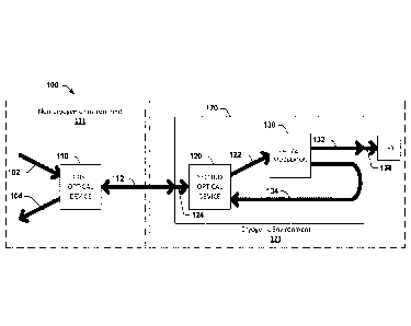
[0015] FIG. 1 illustrates an example system 100 (e.g., ultra-low power
electro-optic cryo-
logic system) to redirect unused light from a cryogenic environment 121 (e.g.,
4-77 K) to a non-
cryogenic environment 111 such as a room temperature environtnent (e.g. 300
K). In an
example, the cryogenic environment 121 is separated from the non-cryogenic
environment 111
via an insulated barrier, e.g., an insulated wall, to facilitate maintaining
the temperature within
the cryogenic environment 121. The system 100 includes a first optical device
110 in the non-
4
CA 03094083 2020-09-14
WO 2019/195015 PCT1US2019/023873
cryogenic environment 111. The first optical device 110 is coupled to a first
optical fiber 102, a
second optical fiber 112 (e.g., a polarization maintaining fiber), and a third
optical fiber 104.
The first optical device 110 receives a light signal on the first optical
fiber 102 and outputs the
light signal on the second optical fiber 112. The first optical device 110
further receives a first
modulated light signal from the cryogenic environment 121 on the second
optical fiber 112 and
outputs the first modulated light signal into the non-cryogenic environment
111 on the third
optical fiber 104. Thus, the second optical fiber 112 is a bi-directional path
utilized to transport
the light signal into the cryogenic environment 121 from the non-cryogenic
environment 111,
and the first modulated light signal into the non-cryogenic environment 111
from the cryogenic
environment 121 to remove or dispose of unwanted and unused light from the
cryogenic
environment 121 into the non-cryogenic environment 111.
[0016] The system 100 further includes a modulator module 170 that is
comprised of a
second optical device 120 in the cryogenic environment 121. The second optical
device 120 is
coupled to the second optical fiber 112 via a first optical waveguide 124, and
is further coupled
to a second optical waveguide 122 and a third optical waveguide 134. The
second optical
device 120 receives the light signal from the first optical device 110 via the
second optical
fiber 112. The second optical device 120 outputs the light signal on the
second optical
waveguide 122. The second optical device 120 also receives the first modulated
light signal via
the third optical waveguide 134 and outputs the first modulated light signal
on the second optical
fiber 112 via the first optical waveguide 124.
[0017] The modulator module 170 further includes an optical modulator 130
(e.g., a 1x2
directional coupler modulator (1x2 DCM), a silicon micro resonator (SMR), or
any other optical
modulator that produces an output signal that can be redirected to the non-
cryogenic
environment 111) in the cryogenic environment 121. Thus, this redirected
output signal is not
dissipated into the cryogenic environment 121. The optical modulator 130 is
coupled to the
second optical waveguide 122, a third optical waveguide 134, and a fourth
optical
waveguide 132. The optical modulator 130 receives the light signal from the
second optical
device 120 via the second optical waveguide 122. The optical modulator 130
modulates this
CA 03094083 2020-09-14
WO 2019/195015 PCT1US2019/023873
received light signal (e.g., with a superconducting electrical signal) to
produce the first
modulated light signal and a second modulated light signal. The optical
modulator 130 outputs
the second modulated light signal to a cryogenic device 190, e.g., a cryogenic
computing system,
within the cryogenic environment 121 that is coupled to the optical modulator
130 via the fourth
optical waveguide 132. In another example, the cryogenic device 190 is part of
a cryogenic
system (not shown) that provides a communication path within the cryogenic
environment 121
and/or conveys signals from within the cryogenic environment 121(0 the non-
cryogenic
environment 111. The fourth optical waveguide 132 is coupled to a third
optical fiber 138 to
provide a data path between the optical modulator 130 and the cryogenic device
190 for the
second modulated light signal. The optical modulator 130 also outputs the
first modulated light
signal to the second optical device 120 via the third optical waveguide 134.
The optical
modulator 130 provides two "pseudo-complimentary" optical outputs in which
substantially no
light is wasted into the substrate of the modulator module 170 and which can
be read out via the
fourth optical waveguide 132 and the third optical fiber 138.
[00181 Thus, the system 100 redirects one of the outputs of the optical
modulator 130, the
first modulated light signal on the third optical waveguide 134, from the
cryogenic
environment 121 into the non-cryogenic environment 111. In particular, the
second optical
device 120 receives the first modulated light signal and outputs the first
modulated light signal
on the second optical fiber 112 on which the first modulated light signal will
pass to the non-
cryogenic environment 111. Thereafter, the first optical device 110 outputs
the first modulated
light signal into the non-cryogenic environment 111 to prevent the first
modulated light signal
from increasing a temperature of the cryogenic environment 121. Moreover, the
system 100
eliminates the need for a second fiber at the output of the second optical
device 120 and the
associated complexity (e.g., mass, connectors, space, etc.), with the example
system 100
redirecting one of the two outputs from the optical modulator 130 of the
system 100 without
affecting performance of the optical modulator 130. Furthermore, the second
optical device 120,
the optical modulator 130, and their associated wavegu ides 122, 124, 132, and
134 are integrated
onto a same substrate, resulting in a diminished loss of light as it moves
between such
6
CA 03094083 2020-09-14
WO 2019/195015 PCT1US2019/023873
components such that nearly all of the first modulated light signal can be
redirected into the non-
cryogenic environment 111.
PM 9] FIG. 2 illustrates another example system 200 (e.g., ultra-low
power electro-optic
cryo-logic system) to redirect unused light from a cryogenic environment 221
to a non-cryogenic
environment 211. The system 200 includes a first 1x2 directional coupler 210
(e.g., an on-chip
integrated optical polarization beam splitter/combiner) in the non-cryogenic
environment 211.
The first 1x2 directional coupler 210 is coupled to a first optical fiber 202,
a second optical
fiber 212 (e.g., a polarization maintaining fiber), and a third optical fiber
204 (e.g., a fast axis).
The first 1x2 directional coupler 210 receives a light signal on a slow axis
of the first optical
fiber 202 and outputs the light signal on the second optical fiber 212. The
second optical
fiber 212 is a polarization-maintaining (PM) fiber and carries polarized
continuous wave (CW)
light along its slow (e.g., horizontal) axis. The first 1x2 directional
coupler 210 further receives
a first modulated light signal on the second optical fiber 212 and outputs the
first modulated light
signal into the non-cryogenic environment 211 via the third optical fiber 204.
Thus, the second
optical fiber 212 is a bi-directional path utilized to transport the light
signal into the cryogenic
environment 221 from the non-cryogenic environment 211, and the first
modulated light signal
into the non-cryogenic environment 211 from the cryogenic environment 221,
with the light
signal being transported into the cryogenic environment 221 on a slow axis of
the second optical
fiber 212 and the first modulated light signal being transported on a fast
axis of the second
optical fiber 212.
[NM In an example, the first optical fiber 202 is a slow axis light
path and the third
optical fiber 204 is a fast axis light path. However, depending upon optical
properties, e.g., a
reflective index of a hirefringent material (e.g.. silica, fluorozirconate,
fluoroaluminate,
chalcogenide glasses, sapphire, polystyrene, acrylic, or any other electro-
optical material) of the
first optical fiber 202 and the third optical fiber 204, in another example
the first optical fiber 202
can be a fast axis light path and the third optical fiber 204 can be a slow
axis light path. The
second optical fiber 212 is both a slow axis light path and a fast axis light
path, with the second
optical fiber 212 providing the slow axis light path from the non-cryogenic
environment 211 to
7
CA 03094083 2020-09-14
WO 2019/195015 PCT1US2019/023873
the cryogenic environment 221 and providing the fast axis light path from the
cryogenic
environment 22110 the non-cryogenic environment 211. Likewise, in another
example the
second optical fiber 212 can provide a fast axis light path from the non-
cryogenic
environment 211 to the cryogenic environment 221 and can provide a slow axis
light path from
the cryogenic environment 221 to the non-cryogenic environment 211.
[0021] The system 200 further includes a modulator module 270 that is
comprised of a
second 1x2 bi-directional coupler 220 (e.g., an on-chip integrated optical
polarization beam
splitter/combiner) in the cryogenic environment 221. The second lx2 bi-
directional coupler 220
is coupled to the second optical fiber 212 via a first optical waveguide 224,
and is further
coupled to a second optical waveguide 222 and a fifth optical waveguide 236.
hi an example,
the second optical waveguide 222 is a slow axis and the fifth optical
waveguide 236 is a fast axis
polarization waveguide. In another example, the second optical waveguide 222
is a slow axis
and the fifth optical waveguide 236 is a slow axis polarization waveguide. The
first and
second 1x2 bi-directional coupler 210 and 220 act as polarization-based
multiplexers/demultiplexers in that they are bi-directional devices and are
used to concurrently
split the light from an input fiber according to its polarization states
(e.g., into vertical and
horizontal) and combine two orthogonally-polarized beams into a single, dual
polarization beam.
In the example of FIG. 2 the first and second 1x2 bi-directional coupler 210
and 220 are
polarized along a slow axis of the system 200 which lies along the horizontal
direction.
[0022] The second 1x2 bi-directional coupler 220 receives the light signal
from the
first I x2 bi-directional coupler 210 via the second optical fiber 212. The
second 1x2 bi-
directional coupler 220 outputs the light signal on a second optical waveguide
222. The
second 1x2 hi-directional coupler 220 also receives the first modulated light
signal via the fifth
optical waveguide 236 and outputs the first modulated light signal on the
second optical
fiber 212 via the first optical waveguide 224. The second 1x2 bi-directional
coupler 220 receives
a light signal via a slow (e.g., horizontal) axis of the second optical fiber
212 and outputs a light
signal via a fast (e.g., vertical) axis of the second optical fiber 212.
8
CA 03094083 2020-09-14
WO 2019/195015 PCT1US2019/023873
[0023] The modulator module 270 further includes an optical modulator 230
(e.g., a lx2
directional coupler modulator, a silicon micro resonator optical modulator, or
any other optical
modulator that produces an output signal that can be redirected to the non-
cryogenic
environment 211) in the cryogenic environment 121. Thus, this redirected
output signal is not
dissipated into the cryogenic environment 121. The optical modulator 230 is
coupled to the
second optical waveguide 222, a third optical wave guide 234 (e.g., a 180
degrees turn
waveguide), and a fourth optical waveguide 232. The optical modulator 230
receives the light
signal from the second lx2 directional coupler 220 via the second optical
waveguide 222. The
optical modulator 230 modulates this received light signal to produce the
first modulated light
signal and a second modulated light signal. The optical modulator 230 outputs
the second
modulated light signal to a cryogenic device 290, e.g., a cryogenic computing
system, within the
cryogenic environment 221 that is coupled to the optical modulator 230 via the
fourth optical
waveguide 232. In another example, the cryogenic device 290 is part of a
cryogenic system (not
shown) that provides a communication path within the cryogenic environment 221
and/or
conveys signals from within the cryogenic environment 221 to the non-cryogenic
environment 211. The fourth optical waveguide 232 is coupled to a third
optical fiber 238 to
provide a data path between the optical modulator 230 and the cryogenic device
290 for the
second modulated light signal. The modulator module 270 further includes a
polarization
rotator 240 that is coupled to the third optical waveguide 234 and the fifth
optical
waveguide 236. The optical modulator 230 also outputs the first modulated
light signal to the
polarization rotator 240 via the third optical waveguide 234. The optical
modulator 230 provides
two "pseudo-complimentary" optical outputs in which substantially no light is
wasted into the
substrate of the modulator module 270 and which can be read out via the fourth
optical
waveguide 232 and the third optical fiber 238.
[0024] The polarization rotator 240 is an optical device that rotates the
polarization axis
of a linearly polarized light beam by an angle of choice. In this example, the
polarization
rotator 240 is a 90 degrees polarization rotator and can be integrated
optically with the third
optical waveguide 234 and the fifth optical waveguide 236. The polarization
rotator 240
9
CA 03094083 2020-09-14
WO 2019/195015 PCT1US2019/023873
receives the first modulated light signal from the optical modulator 230 via
the third optical
waveguide 234, rotates a polarization axis of the first modulated light signal
by about 90 degrees
(e.g., within a 5% tolerance), and outputs the polarization axis rotated
version of the first
modulated light signal to the second 1x2 directional coupler-220. The
polarization rotator 240
outputs the rotated version of the first modulated light signal on the fifth
optical waveguide 236
to a fast axis (e.g., a vertical axis) of the second 1x2 directional coupler
220. Thus, the
system 200 redirects one of the outputs of the optical modulator 230, the
first modulated light
signal on the third optical waveguide 234, from the cryogenic environment 121
to the non-
cryogenic environment 211 to prevent the first modulated light signal from
increasing a
temperature of the cryogenic environment 121. Moreover, the system 200
eliminates the need
for a second fiber at the output of the second optical device 220 and the
associated complexity
(e.g., mass, connectors, space, etc.), with the example system 200 redirecting
one of the two
outputs from the optical modulator 230 of the system 200 without affecting
performance of the
optical modulator 230. Furthermore, the second optical device 220, the optical
modulator 230,
and their associated waveguides 222, 224, 232, 234, and 236 are integrated
onto a same
substrate, resulting in a diminished loss of light as it moves between such
components such that
nearly all of the first modulated light signal can be redirected into the non-
cryogenic
environment 211.
[0025] FIG. 3 illustrates yet another example system 300 (e.g., ultra-low
power electro-
optic cryo-logic system) to redirect unused light from a cryogenic environment
321 to a non-
cryogenic environment 311. The system 300 includes a first optical circulator
310 (e.g., an on-
chip integrated optical circulator) in the non-cryogenic environment 311. The
first optical
circulator 310 is coupled to a first optical fiber 302, a second optical fiber
312 (e.g., a
polarization maintaining fiber), and a third optical fiber 304 (e.g., a fast
axis). The first optical
circulator 310 receives a light signal on a slow axis of the first optical
fiber 302 and outputs the
light signal on a second optical fiber 312. The second optical fiber 312 is a
polarization-
maintaining (PM) fiber and carries polarized continuous wave (CW) light along
its slow (e.g.,
horizontal) axis. The first optical circulator 310 further receives a first
modulated light signal on
CA 03094083 2020-09-14
WO 2019/195015 PCT1US2019/023873
the second optical fiber 312 and outputs the first modulated light signal into
the non-cryogenic
environment 311 via the third optical fiber 304. Thus, the second optical
fiber 312 is a bi-
directional path utilized to transport the light signal into the cryogenic
environment 321 from the
non-cryogenic environment 311, and the first modulated light signal into the
non-cryogenic
environment 31.1 from the cryogenic environment 321, with the light signal
being transported
into the cryogenic environment 321 on a slow axis of the second optical fiber
312 and the first
modulated light signal being transported on a fast axis of the second optical
fiber 312.
[0026] In an example, the first optical fiber 302 is a slow axis light path
and the third
optical. fiber 304 is a fast axis light path. However, depending upon optical
properties, e.g., a
reflective index of a birefiingent material (e.g., silica, fluorozirconate,
fluoroaluminate,
chalcogenide glasses, sapphire, polystyrene, acrylic, or any other electro-
optical material) of the
first optical fiber 302 and the third optical fiber 304, in another example
the first optical fiber 302
can be a fast axis light path and the third optical fiber 304 can be a slow
axis light path. The
second optical fiber 312 is both a slow axis light path and a fast axis light
path, with the second
optical fiber 312 providing the slow axis light path from the non-cryogenic
environment 311 to
the cryogenic environment 321 and providing the fast axis light path from the
cryogenic
environment 321 to the non-cryogenic environment 311. Likewise, in another
example the
second optical fiber 312 can provide a fast axis light path from the non-
cryogenic
environment 31.1 to the cryogenic environment 321 and can provide a slow axis
light path from
the cryogenic environment 321 to the non-cryogenic environment 311.
[0027] The system 300 further includes a modulator module 370 that is
comprised of a
second optical circulator 320 (e.g., an on-chip integrated optical circulator)
in the cryogenic
environment 321. The first and second optical circulators 310 and 320 act as
polarization-based
multiplexers/demultiplexers in that they are bi-directional devices and are
used to simultaneoulsy
split the light from an input fiber according to its polarization states
(i.e., into vertical and
horizontal) and combine two orthogonally-polarized beams into a single, dual
polarization beam.
In the example of FIG. 3 the first and second optical circulators 310 and 320
are polarized along
a slow axis of the system 300 which lies along the horizontal direction.
11
CA 03094083 2020-09-14
WO 2019/195015 PCT1US2019/023873
[0028] The second optical circulator 320 receives the light signal from the
first optical
circulator 310 via the second optical fiber 312. The second optical circulator
320 is coupled to
the second optical fiber 312 via a first optical waveguide 324, and is further
coupled to a second
optical waveguide 322 (e.g., a slow axis) and a third optical waveguide 334
(e.g., a 180 degrees
turn waveguide). The second optical circulator 320 outputs the light signal on
a second optical
waveguide 322. The second optical circulator 320 also receives the first
modulated light signal
via the third optical waveguide 334 and outputs the first modulated light
signal on the second
optical fiber 312 via the first optical waveguide 324. The second optical
circulator 320 receives
a light signal via a slow (e.g., horizontal) axis of the second optical fiber
312 and outputs a light
signal via a fast (e.g., vertical) axis of the second optical fiber 312.
[0029] The modulator module 370 further includes an optical modulator 330
(e.g., a 1x2
directional coupler modulator, a silicon micro resonator, or any other optical
modulator that
produces an output signal that can be redirected to the non-cryogenic
environment 311) in the
cryogenic environment 321. Thus. this redirected output signal is not
dissipated into the
cryogenic environment 321. The optical modulator 330 is coupled to a second
optical
waveguide 322, a fifth optical fiber 332, and a third optical waveguide 334.
In an example, the
optical modulator 330 is implemented on a same integrated circuit chip as the
second optical
circulator 320. The optical modulator 330 receives the light signal from the
second optical
circulator 320 via the second optical waveguide 322. The optical modulator 330
modulates this
received light signal to produce the first modulated light signal and a second
modulated light
signal. The optical modulator 330 outputs the second modulated light signal to
a cryogenic
device 390, e.g., a cryogenic computing system, within the cryogenic
environment 321that is
coupled to the optical modulator 330 via the fifth optical fiber 332. In
another example, the
cryogenic device 390 is part of a cryogenic system (not shown) that provides a
communication
path within the cryogenic environment 321 and/or conveys signals from within
the cryogenic
environment 321 to the non-cryogenic environment 311. The fifth optical
waveguide 332 is
coupled to a fourth optical fiber 338 to provide a data path between the
optical modulator 330
and the cryogenic device 390 for the second modulated light signal. The
optical modulator 230
12
CA 03094083 2020-09-14
WO 2019/195015 PCT1US2019/023873
also outputs the first modulated light signal to the second optical circulator
320 via the third
optical waveguide 334. The optical modulator 330 provides two "pseudo-
complimentary"
optical outputs in which substantially no light is wasted into the substrate
of the modulator
module 370 and which can be read out via the fifth optical waveguide 332 and
the fourth optical
fiber 338.
[00301 Thus, the system 300 redirects one of the outputs of the optical
modulator 330, the
first modulated light signal on the third optical waveguide 334, from the
cryogenic
environment 321 to the non-cryogenic environment 311 where the first modulated
light signal
will not increase a temperature of the cryogenic environment 321. In
particular, the second
optical circulator 320 receives the first modulated light signal and outputs
the first modulated
light signal on the second optical fiber 312 on which the first modulated
light signal will pass to
the non-cryogenic environment 311. Thereafter, the first optical circulators
310 outputs the first
modulated light signal into the non-cryogenic environment 311 to prevent the
first modulated
light signal from increasing a temperature of the cryogenic environment 321.
Moreover, the
system 300 eliminates the need for a second fiber at the output of the second
optical
circulator 320 and the associated complexity (e.g.. mass, connectors, space,
etc.), with the
example system 300 redirecting one of the two outputs from the optical
modulator 330 of the
system 300 without affecting performance of the optical modulator 330.
Furthermore, the
second optical circulator 320, the optical modulator 330, and their associated
waveguides 322, 324, 332, and 334 are integrated onto a same substrate,
resulting in a
diminished loss of light as it moves between such components such that nearly
all of the first
modulated light signal can be redirected into the non-cryogenic environment
311.
[0031] FIG. 4A illustrates an example schematic of an optical modulator 430
(e.g., a 1x2
directional coupler modulator). In an example, the optical modulator 430 can
be used as the
optical modulator 130, the optical modulator 230, and/or the optical modulator
330 illustrated in
FIGS. 1-3, respectively.
[0032] The optical modulator 430 includes a single input, e.g., a single
mode waveguide
input 432. In an example, the optical modulator 430 is implemented on an
electro-optics (EO)
13
CA 03094083 2020-09-14
WO 2019/195015 PCT1US2019/023873
material, such as an organic EO material, a plastic EO material, or a polymer
EO material,
consisting of nonlinear optical chromophores in a polymer lattice. The single
mode
waveguide 432 branches at a waveguide "Y" 434 coupled to a directional coupler
that includes
two substantially identical parallel, single mode coupled waveguides 436 and
440. In an
example, this waveguide "Y" is a slow axis polarization waveguide. Electrodes
450 are disposed
parallel to the two substantially identical parallel, single mode coupled
waveguides 436 and 440.
In an example, the two substantially parallel, single mode coupled waveguides
436 and 440 are
coupled waveguides in that a voltage signal is applied to the electrodes 450
to control the optical
power PI and P2 of the two substantially parallel, single mode coupled
waveguides 436 and 440,
respectively, of the optical modulator 430.
[00331 FIG. 4B illustrates an example optical power timing diagram 460 for
the optical
modulator 430 illustrated in FIG. 4A. In particular, with zero input voltage
(V)) being applied
to the electrodes 450, light coupled into the single mode waveguide 432 splits
evenly between
the two substantially identical parallel, single mode coupled waveguides 436
and 440. In the
case illustrated in FIG. 4B, the output optical power is Pl.P2).5. When a
value of one input
voltage (V=1) is applied to the electrodes 450, a phase mismatch between the
two substantially
identical parallel, single mode coupled waveguides 436 and 440 is introduced,
eliminating
symmetry within the optical modulator 430 and causing unequal splitting of
light at the two
single mode coupled waveguides 436 and 440. Depending on the design of the
optical
modulator 430, one output (e.g., single mode coupled waveguide 436) will be
high (optical
power=1) and the other output (e.g., single mode coupled waveguide 440) will
be low (optical
power =0). In the example of FIG. 4B, when V=1 is applied to the electrodes
450 the optical
power Pi at the single mode coupled waveguide 436 is P1=1 whereas at the same
time the
optical power P2 at single mode coupled waveguide 440 is P2=0. In the example
illustrated, the
optical modulator 430 produces a first modulated light signal at optical power
P1 that is a
complement of the second modulated light signal at optical power P2 produced
by the optical
modulator 430.
14
CA 03094083 2020-09-14
WO 2019/195015 PCT1US2019/023873
[0034] In view of the foregoing structural and functional features
described above, a
method in accordance with various aspects of the present disclosure will be
better appreciated
with reference to FIG. 5. While, for purposes of simplicity of explanation,
the method of FIG. 5
is shown and described as executing serially, it is to be understood and
appreciated that the
present disclosure is not limited by the illustrated order, as some aspects
may, in accordance with
the present disclosure, occur in different orders and/or concurrently with
other aspects from that
shown and described herein. Moreover, not all illustrated features may be
required to implement
a method in accordance with an aspect of the present disclosure. Additionally,
the method of
FIG. 5 may include additional features as described above for the components
described in
FIGS. 1-4.
[0035] FIG. 5 illustrates an example method 500 of redirect unused light
from the
cryogenic environment 121, 221, or 32110 the non-cryogenic environment 111,
211, or 311.
This redirected unused light is not dissipated into the cryogenic environment
121, 221, or 321.
At 505, the method 500 includes outputting, from a first optical device (e.g.,
the first optical
device 110 of FIG. 1, the first lx2 directional coupler 210 of FIG. 2, and
first optical
circulator 310 of FIG. 3) in a non-cryogenic environment 111. 211, or 311, a
light signal to a
second optical device (e.g., the second optical device 120 of FIG. 1, the
second lx2 directional
coupler 220 of FIG. 2, and second optical circulator 320 of FIG. 3) in the
cryogenic
environment 121, 221, or 321. At 510, the method 500 further includes
outputting, from the
second optical device, the light signal to an optical modulator (e.g., optical
modulator 130 of
FIG. 1, optical modulator 230 of FIG. 2, and optical modulator 330 of FIG. 3)
in the cryogenic
environment 121, 221, or 321.
[0036] At 515, the method 500 even further includes modulating, with the
optical
modulator, the light signal to produce a first modulated light signal and a
second modulated light
signal. At 520, the method 500 further includes outputting, from the optical
modulator, the
second modulated light signal. At 525, the method 500 yet further includes
outputting, from the
optical modulator, the first modulated light signal to the second optical
device.
CA 03094083 2020-09-14
WO 2019/195015 PCT1US2019/023873
[0037] At 530, the method even further includes outputting, from the second
optical
device, the first modulated light signal to the first optical device. At 535,
the method 500 yet
further includes outputting, from the first optical device. the first
modulated light signal into the
non-cryogenic environment 111, 211, or 311.
[0038] What have been described above are examples of the disclosure. It
is, of course,
not possible to describe every conceivable combination of components or method
for purposes of
describing the disclosure, but one of ordinary skill in the art will recognize
that many further
combinations and permutations of the disclosure are possible. Accordingly, the
disclosure is
intended to embrace all such alterations, modifications, and variations that
fall within the scope
of this application, including the appended claims.
16