Note: Descriptions are shown in the official language in which they were submitted.
CA 03095456 2020-09-28
WO 2019/191442 PCT/US2019/024601
DEVICES, SYSTEMS, AND METHODS FACILITATING AMBIENT-TEMPERATURE
QUANTUM INFORMATION BUFFERING, STORAGE, AND COMMUNICATION
CROSS-REFERENCE TO RELATED APPLICATIONS
[0001] This application claims the benefit of U.S. Provisional Patent
Application No.
62/649,275, filed on March 28, 2018, U.S. Provisional Patent Application No.
62/696,219, filed
on July 10, 2018, and U.S. Provisional Patent Application No. 62/729,788,
filed on September
11, 2018, the entire contents of each of which is hereby incorporated herein
by reference.
BACKGROUND
Technical Field
[0002] The present disclosure relates to quantum communication and, more
particularly,
to devices, systems, and methods facilitating ambient-temperature quantum
information
buffering, storage, and communication.
Background of Related Art
[0003] Quantum communication technologies can revolutionize the
communications
industry, e.g., the storage, the transmission, and the processing of
information, particularly
because of their ability to enable fully secured communications.
[0004] While robust cryptographic techniques currently exist, these
techniques are
susceptible to hacking, and there is a strong possibility that powerful-enough
computers and
sophisticated hackers could eventually break today's most robust cryptographic
techniques.
Should a means to break these techniques be found, many communications using
these
techniques, including stored past communications, could become vulnerable.
[0005] Contrary to current cryptographic techniques, which are mostly
based on
advanced mathematics, quantum communication is based on the physical laws of
nature, e.g.,
1
CA 03095456 2020-09-28
WO 2019/191442 PCT/US2019/024601
quantum physics. The principles of quantum physics enable the creation of
fundamentally secure
quantum communication techniques such as, for example, Quantum Key
Distribution (QKD).
QKD is a fundamentally secure communication technique where any attempt by an
eavesdropper
to intercept a communication introduces anomalies that can be detected by the
communicating
parties. This results from an essential aspect of quantum mechanics ¨ that the
process of
measuring a quantum system necessarily disturbs the system.
[0006] Despite the significant advantage of being able to provide fully-
secured
communications, quantum communication techniques are not ubiquitous. This is
due, in part, to
the difficulties of counteracting transmission loss in fibers and storing (or
buffering) the quantum
information.
[0007] When transmission over long-distances is required, measures must
be taken to
counteract the unavoidable losses of the transmitted signal. With respect to
traditional
communications, a signal repeater receives, amplifies (or replicates), and
forwards the signal.
However, for quantum communications the solution of a quantum repeater is not
so simple.
Here, the same fundamental physics principle that protects against
eavesdroppers also prevents
the direct amplification of quantum information (qubits).
[0008] Consequently, there is a need for devices, systems, and methods
facilitating
quantum information buffering, storage, and communication. For such devices to
become wide-
spread and be adopted by telecommunication industries, their cost and
operations must be
streamlined. In particular, to be truly scalable, such devices should not use
environment-
controlling systems such as cryogenics, laser, and/or vacuum.
2
CA 03095456 2020-09-28
WO 2019/191442 PCT/US2019/024601
SUMMARY
[0009] The present disclosure provides devices, systems, and methods
facilitating
ambient-temperature quantum information buffering, storage, and communication.
These
devices, systems, and methods enable long-distance transmission of quantum
communications at
ambient temperatures such as for use in Quantum Key Distribution (QKD) links,
quantum
repeaters, and/or other quantum communication networks which involve quantum
memories.
Such devices, systems, and methods match the criteria for mass adoption, field
operation, and
scal ability.
[0010] The devices, systems, and methods of the present disclosure have
advantageous
operation capabilities and technical characteristics in that they, for
example: (1) are comparable
to cryogenic and cold-atom alternatives in terms of technical specifications
(e.g., storage time
and fidelity); (2) work unconditionally (without requiring control changes in
order to store
different polarizations) for arbitrary polarizations of light (enabling
storage of fundamental
particles of light (photons) and the quantum information decoded on the
photons as polarization,
and successful retrieval of the photon polarization with fidelities above
90%); (3) are suitable for
any photon-based quantum application and capable of storing randomized photons
in a shot-by-
shot experiment up to MHz repetition rates, a key feature necessary for any
long-distance
quantum cryptography, quantum secure networks, and quantum repeaters); (4) are
compatible
with both fiber-optics and free-space communication methods (e.g., satellite
to earth
communication) by using a vapor medium that allows the memory to be suitable
for photons with
modified temporal and spatial shapes (e.g., due to the atmospheric noise); (5)
provide portable,
ambient-temperature, plug-and-play quantum memories to enable the
establishment of repeater-
backed quantum networks; and (6) provide scalable, cost-friendly, and
maintenance friendly
3
CA 03095456 2020-09-28
WO 2019/191442 PCT/US2019/024601
quantum memories without the need for cryogenic cooling, laser cooling, and/or
vacuum systems
thereby reducing size, cost, and maintenance considerations.
[0011] The above and other aspects and features of the present disclosure
are detailed
below. To the extent consistent, any of the aspects and features of the
present disclosure may be
utilized in conjunction with (or without) any of the other aspects and
features of the present
disclosure.
[0012] A portable, ambient-temperature operating, quantum memory device
provided in
accordance with aspects of the present disclosure includes an inner structural
frame, an outer
shell surrounding the inner structural frame, a probe input configured to
receive a probe-field
photon beam (anywhere from a continuous light level to single-photon quantum
light pulses)
including quantum information in the form of polarization qubits, a control
input configured to
receive a control-field photon beam for storage and slow-down control, a dual-
rail quantum
memory module disposed within the outer shell (and including a magnetic
shielding structure)
and supported by the inner structural frame, and a filtering module, e.g.,
including a plurality of
filtering components, disposed within the outer shell and supported by the
inner structural frame.
The dual-rail quantum memory module is coupled to the probe input for
receiving the probe-field
photon beam, and coupled to the control input for receiving the control-field
photon beam,
thereby enabling storage of the quantum information within a pair of atomic
vapor cells of a
vapor cell assembly of the dual-rail quantum memory module. The filtering
module is coupled,
e.g., attached, to the dual-rail quantum memory module and configured to
retrieve the quantum
information therefrom. The output of the quantum memory device is configured
to output the
quantum information from the filtering module, e.g., to a processing device.
4
CA 03095456 2020-09-28
WO 2019/191442 PCT/US2019/024601
[0013] In an aspect of the present disclosure, the dual-rail quantum
memory module is
configured to store the polarization encoded (qubit) quantum information as
photons of two
independent photon beams, each of the independent photon beams consisting of a
combined
beam formed from a polarization-split beam of the probe-field photon beam and
a polarization-
split beam of the control-field photon beam.
[0014] In another aspect of the present disclosure, the atomic vapor
cells contain
Rubidium 87 atoms and a buffer gas of, for example, Kr and/or Neon. Other
atoms such as Cs
can also be used instead of Rubidium 87. The vapor cells are parallel to each
other, mechanically
mounted, and controlled in such a way that the temperature is uniform along
their entire length.
[0015] In another aspect of the present disclosure, the dual-rail quantum
memory module
further includes at least two heaters configured to heat the vapor cell and at
least one controller
configured to control and monitor the aforementioned heaters to thereby
control the temperature
of the vapor cells. The heaters are configured in such a way that they
produces no, or minimal,
magnetic fields in the region near the cells.
[0016] In yet another aspect of the present disclosure the heaters and
vapor cells are
shielded by multiple layers of mu-metal to significantly reduce the magnetic
field in the cell
region. This shielding is optimized both in geometrical configuration and
thickness. The multiple
layers of shielding are concentric within each other and assembled in such a
way to permit easy
replacement or removal of the vapor cells.
[0017] In yet another aspect of the present disclosure, the dual-rail
quantum memory
module takes advantage of the phenomena of Electromagnetically Induced
Transparency (EIT)
for storage in both rail, enabling up to 500,us storage time.
CA 03095456 2020-09-28
WO 2019/191442 PCT/US2019/024601
[0018] In still another aspect of the present disclosure, the filtering
module is configured
to retrieve the quantum information as photons of two independent photon
beams. Each of the
independent photon beams is a merged beam formed via a split beam of the probe-
field photon
beam and a split beam of the control-field photon beam portion.
[0019] In still yet another aspect of the present disclosure, the
filtering module is
configured to combine the two independent photon beams into a first beam,
split the first beam
into separate beams, and re-combine the separate beams into a second beam for
output via the
output. This configuration is referred to as dual-rail operation.
[0020] In another aspect of the present disclosure, the filtering module
is configured to
perform filtering before splitting the first beam, between splitting the first
beam and re-
combining the separate beams, and/or after re-combining the separate beams. In
total, this
enables at least 50dB attenuation of the control beam with respect to the
probe photons.
[0021] In an aspect of the present disclosure, a mechanical mounting
layer or board
disposed within the outer shell or casing and supported by the inner
structural frame supports the
quantum memory module and defines a first tier. This layer, e.g., the quantum
memory module,
permits storage of light for either photon packets (classical light pulses) or
for single photons
(qubits). An additional mounting layer or board permits filtering for
retrieval of single photons
and is disposed within the outer shell or casing, supported by the inner
structural frame,
supporting the filtering module thereon, and defining a second tier.
[0022] A method of ambient-temperature quantum communication storage
provided in
accordance with aspects of the present disclosure includes receiving a probe-
field photon beam,
splitting the probe-field photon beam into first and second independent probe
beams, receiving a
control-field photon beam, splitting the control-field photon beam into first
and second
6
CA 03095456 2020-09-28
WO 2019/191442 PCT/US2019/024601
independent control beams, merging the first and second independent control-
field beams with
the respective first and second independent probe beams to provide two
independent, merged
beams, and storing the two independent merged, beams in the quantum memory's
vapor cells.
[0023] In an aspect of the present disclosure, the method further
includes preparing the
control-field photon beam by, for example, matching the wavelength of the
control-field photon
beam with the wavelength of the probe-field photon beam (e.g., phase-lock)
and/or time-
optimizing the control-field photon beam to the probe-field photon beam.
[0024] In another aspect of the present disclosure, the probe-field
photon beam is a
pulsed beam wherein each pulse contains, on average, one photon (qubit).
[0025] In yet another aspect of the present disclosure, when the vapors
cells used are
Rb87 atoms, the probe-field photon beam has a wavelength of 795nm. Other
wavelengths such
as between 780nm and 850nm are also contemplated.
[0026] A method of ambient-temperature output of a stored qubit (quantum
information)
provided in accordance with the present disclosure includes retrieving quantum
information
stored in a quantum memory (wherein the retrieved quantum information is in
the form of two
independent photon beams), combining the two independent photon beams into a
first beam,
splitting the first beam into separate beams, re-combining the separate beams
into a second
beam, and performing filtering before splitting the first beam, between
splitting the first beam
and re-combining the separate beams, and/or after re-combining the separate
beams.
[0027] In still another aspect of the present disclosure, performing
filtering includes
using a Polarization Beam Splitter followed by two Fabry-Perot etalon cavities
and a Faraday
isolator to achieve at least 40dB isolation.
7
CA 03095456 2020-09-28
WO 2019/191442 PCT/US2019/024601
[0028] In another aspect of the disclosure, the Fabry-Perot cavities are
tuned by changing
their length by precisely tuning the temperature of the optical elements using
an automated
tuning scheme. Frequency filtering tuning can additionally or alternatively be
achieve by
precision alignment.
[0029] A method of ambient-temperature quantum communication provided in
accordance with aspects of the present disclosure includes receiving a qubit
(quantum
information) from the probe-field photon beam, splitting the probe-field
photon beam into first
and second independent probe beams, receiving a control-field photon beam,
splitting the
control-field photon beam into first and second independent control-field
beams, merging the
first and second independent control-field beams with the respective first and
second
independent probe-field beams to provide two independent, merged beams,
storing the two
independent, merged beams in a quantum memory vapor cell, retrieving the two
independent,
merged beams from the quantum memory vapor cell, combining the two
independent, merged
beams into a first beam, splitting the first beam into separate beams, re-
combining the separate
beams into a second beam, and performing filtering before splitting the first
beam, between
splitting the first beam and re-combining the separate beams, and after re-
combining the separate
beams.
BRIEF DESCRIPTION OF THE DRAWINGS
[0030] Various aspects and features of the present disclosure are
described hereinbelow
with reference to the drawings wherein like numerals designate similar
elements in each of the
several views and:
8
CA 03095456 2020-09-28
WO 2019/191442 PCT/US2019/024601
[0031] FIG. 1 is a perspective view of a quantum memory device provided
in accordance
with the present disclosure, illustrated as rack-mountable and including three
fiber inputs/outputs
(probe input, control input, and output);
[0032] FIG. 2 is a perspective view of the quantum memory device of FIG.
1 with the
outer shell removed to illustrate the internal components and features
therein;
[0033] FIG. 3A is a block diagram of the quantum memory device of FIG. 1
illustrating
storage and filtering modules thereof;
[0034] FIG. 3B is a schematic diagram of the quantum memory device of
FIG. 1
illustrating the storage and filtering modules thereof;
[0035] FIG. 3C is a side view of the storage and filtering modules of the
quantum
memory device of FIG. 1;
[0036] FIG. 3D is a four-level scheme for Rubidium 87 illustrating the
transitions
thereof;
[0037] FIG. 4 is a corner, partial section view, with portions of the
outer shell removed to
show the inside of the quantum memory device of FIG. 1;
[0038] FIG. 5 is a side, cross-sectional view, with the outer shell
removed, of the
quantum memory device of FIG. 1; and
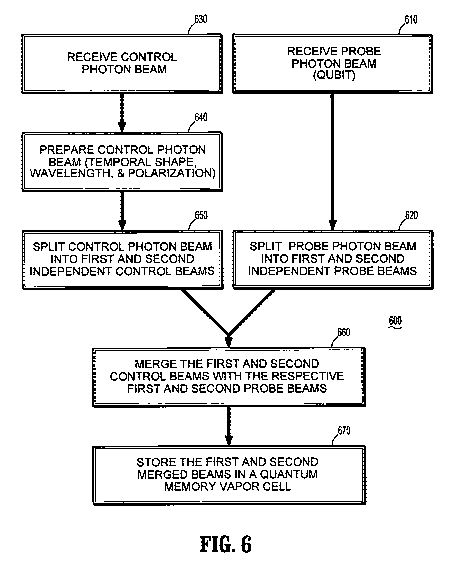
[0039] FIG. 6 is a flow diagram illustrating a first (preparation &
storage) portion of a
method of the present disclosure;
[0040] FIG. 7 is a flow diagram illustrating a second (filtering &
retrieval) portion of a
method of the present disclosure;
[0041] FIG. 8 is a rear, bottom, perspective view of the quantum memory
device of FIG.
1;
9
CA 03095456 2020-09-28
WO 2019/191442 PCT/US2019/024601
[0042] FIG. 9 is an exploded, perspective view of the internal components
of the
quantum memory device of FIG. 1;
[0043] FIGS. 10-14 are various views of the vapor cell assembly of the
quantum memory
device of FIG. 1;
[0044] FIGS. 15-18 are top perspective, top plan, bottom plan, and bottom
perspective
views, respectively, of the first tier of the quantum memory device of FIG. 1;
[0045] FIGS. 19 and 20 are top perspective and top plan views,
respectively, of the
second tier of the quantum memory device of FIG. 1;
[0046] FIG. 21 is a rear perspective views of the of the quantum memory
device of FIG.
1 with the outer shell removed and certain supporting structures shown in
phantom;
[0047] FIG. 22 is a schematic diagram of device(s) for generating the
probe-field photons
and a control-field photon beam for the quantum memory device of FIG. 1;
[0048] FIG. 23 is a simplified, schematic diagram of an exemplary quantum
network
provided in accordance with the present disclosure;
[0049] FIG. 24 is a flow diagram illustrating a method of a quantum
network of the
present disclosure; and
[0050] FIG. 25 is a block diagram illustrating a control system
configured for use with
the quantum memory device of FIG. 1.
DETAILED DESCRIPTION
[0051] The following detailed description is made with reference to the
accompanying
drawings, wherein explanations regarding components, functions, or
constructions known in the
art are summarily provided or omitted entirely in an effort to avoid obscuring
the aspects and
features of the present disclosure with unnecessary details. In addition, any
particular values or
CA 03095456 2020-09-28
WO 2019/191442 PCT/US2019/024601
ranges detailed herein are understood to encompass variations within limits
generally accepted in
the art, wherein such variations are due to, for example, margins of error in
measurement and/or
feedback-based control systems, material and system margins of error and
tolerances,
environmental conditions, manufacturing tolerances, etc.
Quantum Memory
[0052] Referring to FIGS. 1-3C, an ambient-temperature quantum memory
device in
accordance with the present disclosure is shown and generally identified by
reference numeral
10. For the purposes herein, "ambient temperature" refers to temperatures that
are not controlled
for the purpose of quantum storage/communication, e.g., non-laboratory-
controlled temperatures,
temperatures not influenced by one or more of cryogenic cooling systems, laser
cooling systems,
vacuum systems, etc. "Ambient temperatures" may include room temperatures,
environment
temperatures (e.g., 0 C to 100 C), or the like. The main challenges for
developing such an
ambient-temperature quantum memory device 10 are defeating the inherent strong
atomic
motion, de-coherence, and noise, e.g., background photons, without the need
for extreme cooling
or vacuum systems. Quantum memory device 10, described in detail below,
overcomes these
challenges.
[0053] Quantum memory device 10 is configured to: 1) receive, at an input
"I" (FIG.
3A), a quantum communication such as, for example, photons storing quantum
information, e.g.,
polarization qubits; 2) store the photons within quantum memory module 100
thereof; 3)
selectively retrieve the photons and perform filtering via filtering module
200; and 4) send the
photons as a quantum communication from an output "0." Quantum memory device
10, more
specifically, allows for independent channels performing Quantum Key
Distribution (QKD)
using the BB84 protocol and polarization qubits; works with arbitrary
polarization qubits with
11
CA 03095456 2020-09-28
WO 2019/191442 PCT/US2019/024601
retrieval fidelities greater than 90% and with fidelities greater than 98%
upon using the auxiliary
field filtering scheme detailed below; provides for the storage of randomized
photons in a shot-
by-shot manner; and enables creation of a long-distance quantum secure network
utilizing one or
more of such quantum memory devices 10 at ambient-temperatures and outside the
controlled
laboratory setting.
[0054] Quantum memory device 10, as illustrated in FIGS. 1, 2, and 4,
includes an outer
shell 12 and an inner structural frame 14 disposed within outer shell 12.
Outer shell 12 is at least
partially formed from, or coated with, magnetic shielding material to inhibit
electromagnetic
interference passing through outer shell 12. Inner structural frame 14
supports the operable
internal modules of quantum memory device 10: quantum memory module 100 and
filtering
module 200. Inner structural frame 14 includes a plurality of vibration
dampeners 15, e.g.,
shock-mount coils and grommets, configured to inhibit or at least dampen
external vibrations
from reaching the internal operating components and optical elements of
quantum memory
device 10.
[0055] Referring to FIGS. 3A-3C, quantum memory module 100 and filtering
module
200 are detailed. For the purposes of brevity, features and components known
in the art and not
germane to the understanding of quantum memory module 100 and filtering module
200 are not
described herein such as, for example, lenses, mirrors, etc., as it is
understood that a person of
skill in the art would readily understand how to implement and utilize such
components, as
necessary, in making and using quantum memory module 100 and filtering module
200. Further,
various different configurations and ordering of components may be provided
without departing
from the scope of the present disclosure as illustrated and/or detailed
herein.
12
CA 03095456 2020-09-28
WO 2019/191442 PCT/US2019/024601
[0056] As best shown in FIG. 3B, and with additional reference to FIGS.
15-17, and 21,
quantum memory module 100 is configured as an Electromagnetically Induced
Transparency
(EIT) based quantum memory and includes a probe input 110 configured to
receive a quantum
communication in the form of a photon beam, from input "I." The photon beam,
referred to as
the probe-field photon beam, may be pulsed, with each pulse on average
containing one (1)
qubit, and a wavelength of 795nm, although other suitable wavelengths or
wavelength ranges are
also contemplated, e.g., wavelengths between 780nm and 850nm. The probe-field
photon beam
can be produced, for example, by extreme attenuation of a laser beam or
through various optical
processes such as parametric down conversion or single photon sources (e.g.,
quantum dots). An
exemplary probe-field photon beam preparation configuration is detailed below
with respect to
FIG. 22.
[0057] A first beam displacer 120 splits the probe-field photon beam into
two
orthogonally polarized probe-field photon beams, which are parallel to and
independent of one
another. The first beam displacer 120 may be a birefringent crystal that
allows the vertical
component of a polarization to pass straight through while displacing the
horizontal
component. Between the input 110 and the first beam displacer 120, a plurality
of rotating wave
plates may be provided to compensate for the unitary polarization rotation of
the optical
fiber providing the input photon beam to probe input 110. A half wave plate
124 positioned
after the first beam displacer 120 rotates the polarization of one of the
beams to enable both
beams, or rails, to pass through a first Glan-Thomson polarizing beam splitter
145 and into the
atomic vapor cell assembly 160, as detailed below.
[0058] Quantum memory module 100 further includes a control input 130
configured to
receive a control-field photon beam that is pulsed, in the order of a few mW,
and of the same or
13
CA 03095456 2020-09-28
WO 2019/191442 PCT/US2019/024601
nearly (within acceptable limits) the same wavelength as the probe-field
photon beam, and time-
optimized to the probe-field photon beam. One configuration of the preparation
of the control-
field photon beam and a configuration of input preparation to achieve
resonance, the same
wavelength, and time-optimization between the probe-field photon beam and the
control-field
photon beam are detailed below with respect to FIG. 22.
[0059] The control-field photon beam, upon receipt, may be passed through
a telescope
(not shown in FIG. 3B) to ensure that the control field rails fully cover the
probe rails.
Thereafter, the control-field photon beam is directed through a plurality of
wave plates 134 to a
second beam displacer 140 which splits the control-field photon beam into two
control-field
photon beams, which are parallel to and independent of one another; each
control-field photon
beam corresponding to one of the probe-field photon beams. The control-field
photon beams are
directed to the first Glan-Thomson (or other suitable type) polarizing beam
splitter 145 which
merges the control-field photon beams with the corresponding probe-field
photon beams. A half
wave plate 144 rotates the polarization of one of the beams prior to enable
both beams, or
rails, to pass through the first Glan-Thomson polarizing beam splitter 145 and
into the atomic
vapor cell assembly 160, as detailed below.
[0060] The parallel and independent pairs of photon beams (each formed
via the merger
of a control-field photon beam and a probe-field photon beam) are directed
through the first
telescope 150 to match beam-sizes to that of the vapor cells 161 and then to
an atomic vapor cell
assembly 160. The vapor cell assembly 160 contains two atomic vapor cells 161
(see FIG. 14)
containing atoms of a radioactive isotope, such as Rubidium (Rb), particularly
the isotope 'Rb,
and a buffer gas, such as Krypton (Kr) and/or Neon (Ne). The control-field
photon beams enter
the vapor cell assembly 160 to prepare the two vapor cells 161, two
independent volumes which
14
CA 03095456 2020-09-28
WO 2019/191442 PCT/US2019/024601
serve as the storage mediums for storing the photons of the respective probe-
field photon beams
and allowing these photons to be stored and retrieved with variable, and
controllable, storage
times. With momentary additional reference to FIGS. 10-14, vapor cell assembly
160 includes,
around it, three layers of concentric magnetic shielding material, for
example, Mu shielding 162
(layers 163a, 163b, 163c) to surround and maintain a magnetically neutral
medium around vapor
cell assembly 160, one or more, e.g., two, heaters 164 (see FIGS. 12 and 14,
shown as heating
pads), and a Proportional-Integral-Derivative (PD) controller 166 (FIG. 3B)
running a PID
control loop to control heater(s) 164 to maintain a suitable temperature of
the vapor cells 161 of
vapor cell assembly 160, e.g., of 55 C to 70 C or, in embodiments, 60 C to
about 70 C. A
safety circuit (not shown) is also used to prevent overheating. Vapor cell
assembly 160 is
mounted depending from third board 20 via a plurality of brackets 168 and a
plurality of
vibration dampeners 169 (FIG. 10). Brackets 168 define a plurality of fins
that act as heat sinks
to dissipate excess heat away from surrounding optical elements. Centrally
positioning vapor cell
assembly 160 helps maintain a constant temperature thereof and provides
increased shock,
misalignment, and damage protection (which is furthered by vibration dampeners
169).
[0061] The above-detailed parallel and independent pairs of photon beams
provide a
dual-rail EIT quantum memory enabling any arbitrary polarization of photons to
be mapped onto
a quantum superposition of the two spatially-separated and independent
"rails." This allows the
preservation of the polarization while the individual photons are stored.
[0062] On the retrieval side of vapor cell assembly 160, for when the
stored photons are
desired to be retrieved (which may be on-demand, including storage times of up
to 500,us),
quantum memory module 100 includes a second telescope 170 which directs the
retrieved
photon beams through a plurality of wave plats 164 to a second Glan-Thomson
(or other
CA 03095456 2020-09-28
WO 2019/191442 PCT/US2019/024601
suitable) polarizing beam splitter 180 to filter the control field based on
the polarization, e.g., to
separate the vertically polarized control field photons from the horizontally
polarized probe
pulses. A beam dump 185 collects the undesired portion of the retrieved photon
beams from
second Glan-Thomson polarizing beam splitter 180, while the desired portion of
the retrieved
photon beams from second Glan-Thomson polarizing beam splitter 180 are
directed through a
half wave plate 184 to a third beam displacer 190, working in the opposite
direction as first and
second beam displacers 120, 140, such that third beam displacer 190 combines
the pair of the
retrieved photon beams into a single retrieved photon beam. The single
retrieved photon beam
can be extracted for classical light storage, or can be directed to the
filtering module 200. Note
that, in some embodiments, second telescope 170, second Glan-Thomson
polarizing beam
splitter 180, beam dump 185, and third beam displacer 190 are characterized as
part of the
filtering module 200.
[0063] Continuing with reference to FIG. 3B, and with additional
reference to FIGS. 19-
21, the filtering module 200 receives the retrieved photon beam (which
includes both probe
photons and the remaining attenuated control portions) and is configured to
eliminate the
remainder of the control-field photon beam, e.g., the 1012 unwanted photons of
the control field,
as well as the noise which is present at ambient temperatures, all without
damaging the
information-carrying probe-field photon beam. The single retrieved photon beam
received from
quantum memory module 100 is directed to a first frequency filter (e.g., a PID
temperature-
controlled >50 dB Fabry-Perot cavity, filter, or etalon) 210, then to a fourth
beam displacer 220
to split the beam. The split beam is then provided to a polarization
maintaining magnetic Faraday
isolator filter 230 (ensuring the preservation of information encoded on the
photons throughout
the filtering module 200 for any arbitrary polarization qubit) and, from
there, to a fifth beam
16
CA 03095456 2020-09-28
WO 2019/191442 PCT/US2019/024601
displacer 240 in an opposing direction as fourth beam displacer 220 to rejoin
the split beam into
a single photon beam. The photon beam is then directed to a second frequency
filter (e.g., a PID
temperature-controlled >50 dB Fabry-Perot cavity, filter, or etalon) 250 and,
ultimately, through
a plurality of wave plates 254 to output 260 of quantum memory device 10. The
Fabry-Perot
cavities 210, 250 (as well as other temperature-sensitive components of
quantum memory device
10), are thermally-isolated from heat-generating components by way of plural
thermal barriers
290 (FIG. 5); they are also vibration dampened via the various vibration
dampeners, e.g.,
vibration dampeners 15 (FIG. 4), and the configuration of inner structural
frame 14. Further, fans
26 (see FIG. 8) are utilized to draw heat out of the interior of quantum
memory device 10 and,
more specifically, are positioned to help ensure temperature stabilization of
Fabry-Perot cavities
210, 250 (and/or other temperature-sensitive components of quantum memory
device 10). Fans
26 may be controlled by the PID controllers of Fabry-Perot cavities 210, 250
to ensure precise
temperature control thereof, as noted below.
[0064] The filtering module 200 suppresses the control-field photon beam,
having
demonstrated the ability to provide a total probe-field transmission of 5 %
for all polarization
inputs, exhibiting an effective, control-to-probe suppression ratio of 130 dB,
thereby effectively
eliminating the control-field photon beam. Further, ¨50dB of control field
extinction is achieved.
Fine tuning of the transmission frequency is accomplished by controlling the
temperatures of the
passive frequency filters 210, 250 (which may have free spectral ranges (FSRs)
of 210-220GHz to
minimize the transmission of the control field, which is phase-locked at an
offset 6.834GHz from
the probe field) using the independent PID controllers with a precision of
equal to or less than
0.1K.
17
CA 03095456 2020-09-28
WO 2019/191442 PCT/US2019/024601
[0065] The filtering module 200 and the quantum memory module 100 also
reshape
noise, of which the leading source for EIT-based quantum memory devices comes
from
spontaneous four-wave mixing, which induces unwanted gain on the probe
wavelength. The
filtering module 200 and the quantum memory module 100, more specifically,
cooperate to
effect noise reduction by introducing an auxiliary optical field that
destructively interferes with
the Stokes field generated by four-wave mixing within the 87RB vapor cells of
vapor cell
assembly 160, thereby creating a substantial signal-to-background ratio after
the frequency
filtering. This noise reduction enables fidelities greater than 98%. However,
other suitable noise
filtering schemes are also contemplated. A safety circuit (not explicitly
shown) is also provided
to prevent under-cooling of the etalons 210, 250 to avoid reaching the dew
point, preventing
condensation on their surfaces.
[0066] Turning now to FIGS. 3C-5 and 8-21, quantum memory device 10 is
embodied as
a robust, ambient-temperature operating device configured for use outside the
laboratory as part
of a quantum network including plural of such devices and/or other suitable
quantum networking
components. For the purposes herein, "portable" refers to a device that is
capable of being lifted,
transported, and deployed in the field (e.g., rack-mounted) without
significant ancillary
equipment or infrastructure ¨ as opposed to laboratory operating quantum
memories which
reside on optical tables. The portability aspect, combined with ambient-
temperature operation,
promotes scalability contrarily to alternatives, which require cryogenic
cooling, laser cooling,
and/or vacuum systems.
[0067] Quantum memory device 10 includes various sub-assemblies
supporting the
various components of quantum memory module 100, filtering module 200, and the
other
functional components (e.g., controllers, power sources, sensors, storage
devices, etc.) associated
18
CA 03095456 2020-09-28
WO 2019/191442 PCT/US2019/024601
with modules 100, 200. These sub-assemblies are disposed within shell 12 and
supported by
inner structural frame 14 in a manner that provides robustness, optical
stability, long-term
operation, and that promotes modularization. More specifically, the quantum
memory device 10
includes a first, upper tier 16 having the various components of quantum
memory module 100
and a second, lower tier 18 having the various components of filtering module
200. A first
mechanical mounting layer or board 17 forming the first tier 16 includes the
components of the
quantum memory module 100 mounted thereon and depending therefrom, with vapor
cell
assembly 160 seated within a central opening defined through first board 17
(FIG. 2). A second
mechanical mounting layer or board 19 forming the second tier 18 includes the
components of
filtering module 200 mounted thereon. A third mechanical mounting layer or
board 20 serves as
a top of the inner structural frame 14 and mounts atomic vapor cell assembly
160 thereon with
atomic vapor cell assembly 160 depending therefrom. With third board 20
positioned in this
manner, the components of the quantum memory module 100 and filtering module
200 are
disposed between second and third boards 19, 20, respectively, with first
board 17 generally
centrally disposed relative thereto. Corner pillars 22 are provided to provide
structural support
and maintain proper spacing between the board 17, 19, 20 and, thus, the
components of quantum
memory module 100 and filtering module 200.
[0068] Referring in particular to FIGS. 4 and 8, shell 12 may include
slide brackets 24
disposed on opposite sides thereof to enable quantum memory device 10 to be
rack mounted,
e.g., quantum memory device 10 may be sized for use with a standard 19-inch
rack, although
other configurations are also contemplated. As shown in FIGS. 8, 19, and 21,
fans 26 may be
mounted to depend from shell 12; fans 26, as appreciated, facilitate cooling
of the electronic
components of quantum memory device 10 and exhaust externally of the interior
of shell 12. In
19
CA 03095456 2020-09-28
WO 2019/191442 PCT/US2019/024601
embodiments, fans 26 are positioned adjacent, e.g., depending below, Fabry-
Perot cavities 210,
250 to maintain stable temperatures thereof, as noted above (see FIGS. 8 and
9). Continuing with
reference to FIG. 8, the rear (or one or more other portions) of quantum
memory device 10
further includes an AC power receptacle 29a, an ON/OFF power button 29b, one
or more USB
or other suitable ports 29c for monitoring, tuning, and/or controlling quantum
memory device 10,
a plurality of heat sink fins 29d configured to help dissipate heat, e.g.,
from the power source,
and a temperature control panel 29e configured to enable external monitoring
and/or control of
the temperature of vapor cells 161 of vapor cell assembly 160 (see FIGS. 10-
14).
[0069] With reference to FIG. 6, a method 600 facilitating ambient-
temperature quantum
communication such as, for example, using quantum memory device 10 (FIG. 1) or
any other
suitable quantum memory device is detailed. Method 600 includes, at 610,
receiving a probe-
field photon beam (qubit) and, at 620, splitting the probe-field photon beam
into first and second
independent (and orthogonally polarized and parallel) probe beams. At the same
time or in close
temporal relation, a control-field photon beam is received at 630, prepared at
640, e.g., for
temporal shape, wavelength, and polarization, and split at 650 similar as with
the probe-field
photon beam. At 660, the first and second control beams are merged with the
respective first and
second probe beams to provide two independent, merged beams (each having a
control beam
component and a probe beam component). The independent, merged beams are then
directed to a
quantum memory vapor cell for storage therein, as indicated at 670. The above-
detailed method
enables selective retrieval of the independent, merged beams, as detailed
below.
[0070] Turning to FIG. 7, method 700 is provided to retrieve and output
the stored
quantum communication. In method 700, independent beams stored in the quantum
memory's
vapor cell are retrieved at 710 (where these two beams are merged; both beams
have a control-
CA 03095456 2020-09-28
WO 2019/191442 PCT/US2019/024601
field component and a probe-field component). The two independent beams are
combined at
720, filtered at 730, split at 740, filtered again at 750, and re-combined at
760. Finally, at 770,
the stored quantum communication (qubit) is retrieved from the quantum memory.
This process
eliminates noise from the control-field beam without damaging the probe-field
photon beam, and
the quantum information it carries. Ultimately, once filtered as noted above,
the resultant photon
beam is output for transmission to another device, component, or system.
Qubit Preparation
[0071] Referring to FIG. 22, an exemplary device for generating the probe-
field photon
beam and control-field photon beam for input to memory 10 (FIG. 1) is shown
generally
identified by reference numeral 900 including a laser preparation module 910
and an input
preparation module 960. The laser preparation module 910 includes a first
diode laser 912 used
for generating the probe-field photon beam which is controlled using a PID
lock 914 and a
compact saturation spectroscopy (Doppler free spectroscopy) system 916, e.g.,
a Toptica CoSy
system, available from Toptica Photonics, Inc. of Farmington, NY, USA. An
acousto-optic
modulator (AOM) 918 is positioned before the locking beam enters the system
916.
[0072] The control-field photon beam, generated by a second diode laser
920, is locked
to transmit light at a specific frequency, e.g., 6.8348 GHz, away from the
probe-field photon
beam using a PID phase lock 922 and mixing with signals from a frequency
generator 924 and a
function generator 926.
[0073] Having been generated as detailed above, the probe-field photon
beam and the
control-field photon beam are transmitted from the laser preparation module
910 to the input
preparation module 960 to be shaped before entering the memory 10 (FIG. 1). An
FPGA-
controlled DAC (or Arbitrary Wave Generator) 962, controlled by a master
trigger (QC)
964, sets the repetition rate of the probe-field photon beam and generates one
FWHM
21
CA 03095456 2020-09-28
WO 2019/191442 PCT/US2019/024601
Gaussian envelope per trigger. This pulse is then sent to an AOM driver 966 as
the
Amplitude Modulation (AM) input to an AOM 968 while a frequency modulation
(FM)
input provided by a Signal Generator (SG) 970 is also provided to the AOM 968
to shape
the probe-field photon beam. The control-field photon beam is likewise shaped
via an AOM
972 driven by an AOM drive 974 that receives an AM input from QC 964 and an FM
input
from an SG 976 that is closed to SG 970. These beams are then transmitted to
the memory
(FIG. 1). The probe photons are heavily attenuated such that they average to n
= 1.
Alternatively, a genuine single photon source could be used.
Quantum Network
[0074] Turning to FIGS. 23 and 24, a quantum network requires several
quantum nodes,
capable of coherently manipulating the quantum information with fidelity near
unity such that
the output of each node is indistinguishable from the input provided thereto.
These nodes may
include, for example, one or more quantum memories, quantum simulators, random
number
generators, entanglement sources, and/or photon gates.
[0075] One example of such a quantum network and method leverages room-
temperature
quantum memories, e.g., a plurality of memories 10, to provide a multi-node
memory-assisted
quantum network using polarization qubits. A basic configuration of such a
network, designated
generally as network 1000, includes two polarization qubit sources 1100, two
room-temperature
quantum memories 10 (as detailed above) each connected to a respective one of
the polarization
qubit sources 1100 via a connection 1200, e.g., a fiber-optic cable or other
suitable connection
(including free space connections), and one Bell-state measurement station
1300 employing four
single-photon detectors 1310. Hong-Ou-Mandel (HOM) interference experiments
have verified
identical storage and retrieval from the two room-temperature quantum memories
10 of this
network 1000, e.g., that both the temporal envelope, optical frequency, and
polarization of the
retrieved photons remain the same after storage.
22
CA 03095456 2020-09-28
WO 2019/191442 PCT/US2019/024601
[0076] The polarization qubit sources 1100, more specifically, include
independent laser
diodes 1102 and utilize acousto-optical and electro-optical modulators 1110,
1120, respectively,
to generate random streams of polarization qubits at steps 2710, 2712 of
method 2700. More
specifically, the diodes 1102 generate beams and independent acoustic-optical
modulators
(AOMs) 1110 that temporally shape the probe fields. The AOMs 1100 are driven
by two phase-
locked signal generators. Two DACs (or Arbitrary Wave Generators) modulate the
amplitude of
the AOMs 1110. These DACs (or Arbitrary Wave Generators) are triggered by the
master trigger
FPGA to generate the FWHM Gaussian envelope of the probe pulses. Independent
Electro-
Optical Modulation units (EOM) 1120 are in place to encode the desired
polarization states on
the probe pulses. The output polarization is modulated based on the input
applied voltage to the
E0Ms 1120. An FPGA-based circuit controls the high-voltage amplifiers for fast
operation and
trigger- synchronized control. The FPGA can be programmed to generate any
sequence of
polarizations including a fully (quantum) random sequence. Both probe-field
beams and control-
field beams are delivered from the polarization qubit sources 1100 to the
respective memories 10
via connections 1200, e.g., single-mode optical fibers, as indicated at steps
2720, 2722 of method
2700.
[0077] The beams travel through the connections 1200 to the memories 10
where, as
detailed above, the qubits are stored on a pair of independent dual-rails for
each memory 10, as
indicated at steps 2730, 2732 of method 2700. More specifically, the qubits
are stored according
to method 600 (FIG. 6). After storage, the qubits are retrieved, as indicated
at steps 2740, 2742
of method 2700, e.g., according to method 700 (FIG. 7), temporal wave-function
matching is
performed, and the retrieved qubits are sent to Bell-state measuring station
1300, as indicated at
steps 2750, 2752 of method 2700. Bell-state measuring station 1300 projects
the incoming
23
CA 03095456 2020-09-28
WO 2019/191442 PCT/US2019/024601
retrieved qubits into a Bell-state, as indicated at step 2760 of method 2700.
More specifically, a
series of waveplates are used to compensate for polarization rotation caused
by propagation in
the optical fibers. The pulses retrieved from the memories 10 are interfered
at a 50:50 beam
splitter, and two single-photon detectors (SPCMs) placed at the output arms of
the beam splitter
generate a signal every time they record a hit. Data from the SPCMs is
analyzed to calculate the
coincidence rate between opposite output arms of the NPB S.
[0078] The quantum networks of the present disclosure may further include
a software-
defined infrastructure to monitor and control the devices of the quantum
network to ensure high
efficiency, control, and longevity. In particular, the memories 10 (FIG. 1),
which include feedback
systems for optical filtering, temperature monitoring for the Rb cells, power
monitoring, and
other parameters, can be controlled over the network. Additionally, for self-
turning purposes and
network performance analysis, machine learning or other artificial
intelligence protocols may be
implemented to optimize operating parameters.
[0079] More specifically, with reference to FIG. 25, an embodiment of a
control system
3000 configured to remotely control optimization and operation of quantum
memory device 10 is
shown. Although illustrated with respect to one quantum memory device 10, it
is contemplated
that control system 3000 may enable remote control optimization and operation
of a plurality of
quantum memory devices 10 (and/or other quantum devices) across one or more
quantum
networks. Control system 3000 includes a plurality of sub-systems: on-demand
feedback sub-
system 3010, machine learning sub-system 3020, and quantum/classical feedback
sub-system
3030. Portions of control system 3000 may be implemented using FPGA devices
for fast
feedback control and hybrid quantum/classical controls for system
stabilization (e.g.,
24
CA 03095456 2020-09-28
WO 2019/191442 PCT/US2019/024601
polarization in the transmission fibers) and automation (e.g., noise removal
at single-photon
levels).
[0080] On-demand feedback sub-system 3010 of control system 3000 includes
control
of: the PID controllers and fans 26 (FIGS. 8 and 9) associated with filter
cavities 210, 250 (see
FIG. 3B) to stabilize the temperatures of cavities 210, 250; the PID
controller 166 and heaters
164 for controlling the temperature of the vapor cell assembly 160 (see FIG.
3B); mode-
matching feedback; automatic alignment optimization of the optical components;
and overall
system status monitoring (including, for example, intrusion detection,
protection shutters for
side-channel attacks, implementing decoy states, etc.).
[0081] Machine learning sub-system 3020 optimizes pulse shaping and
timing (spatial
and temporal tuning of pulse parameters), and noise cancelling (implementing
an ultra-low noise
single photon storage regime). Machine learning sub-system 3020 may implement
one or more
of: supervised learning, semi-supervised learning, unsupervised learning,
reinforcement learning,
association rule learning, decision tree learning, anomaly detection, feature
learning, etc., and
may be modeled as one or more of a neural network, Bayesian network, support
vector machine,
genetic algorithm, etc.
[0082] Quantum/classical feedback sub-system 3030 provides: automated,
near-real time
polarization and power measurements and stabilization; noise cancelling
(implementing an ultra-
low noise single photon storage regime); and feedback-based control of the
quantum random
number generator and information encoding. Pulse shaping and timing may
additionally or
alternatively be implemented in quantum/classical feedback sub-system 3030
and, in such
embodiments, enables control and monitoring of light input into and output
from quantum
CA 03095456 2020-09-28
WO 2019/191442 PCT/US2019/024601
memory device 10 as well as how long the light is stored in quantum memory
device 10. Such
may include an FPGA SoC (single-board computer).
[0083] Persons skilled in the art will understand that the features
specifically described
hereinabove and shown in the associated figures are non-limiting exemplary
embodiments, and
that the description, disclosure, and figures should be construed merely as
exemplary of
particular embodiments. Therefore, it is to be understood that the present
disclosure is not limited
to the precise embodiments described, and that various other changes and
modifications may be
made by one skilled in the art without departing from the scope or spirit of
the disclosure.
26