Note: Descriptions are shown in the official language in which they were submitted.
CA 03095974 2020-10-02
WO 2019/219733
PCT/EP2019/062442
1
SENSOR UNIT, RADIATION DETECTOR AND METHOD OF
MANUFACTURING A SENSOR UNIT
Technical Field
The present disclosure generally relates to a sensor unit for a radiation
detector. In particular, a sensor unit for a radiation detector, a radiation
detector comprising at least one sensor unit, and a method of manufacturing
a sensor unit, are provided.
Background
Direct conversion radiation detectors utilize photoconductors, such as a
cadmium telluride (CdTe) conversion element, to capture and convert
incident X-ray photons directly into electrical charge. Photoconductor sensor
modules cannot be made arbitrarily large. For this reason, a large radiation
detector needs to be built from smaller sensor modules. The smaller sensor
modules need to be electrically connected to power and readout circuits. In
some implementations, standard connections are made with wire bonding
from one or more sides of an electronics layer, such as a readout application-
specific integrated circuit (ASIC) substrate. Thereby, input and output (I/O)
signals can be routed to and from the electronics layer. However, this
solution imposes a limitation on the maximum achievable size of the
radiation detector.
In order to cover the exposed wire bonding area, it is possible to provide a
radiation detector comprising tilted sensor modules such that the wire
bonding area of one sensor module is covered by the conversion element of
an adjacent sensor module. In this way, gaps between the sensor modules in
an imaging plane can be avoided. However, this solution is complicated and
gives different distances to an object to be imaged for different positions of
the detector. Furthermore, the radiation angle is increased and shadows may
arise.
CA 03095974 2020-10-02
WO 2019/219733
PCT/EP2019/062442
2
Summary
As an alternative to wire bonding from one or more sides of an electronics
layer, the connections of the sensor modules to power and readout circuits
can be made through the readout ASIC substrate by means of vias. The vias
are often referred to as through silicon vias (TSV) although they may be
fabricated in substrates of materials other than silicon. In this case, the
connections are made on the backside (with reference to the conversion
element). Smaller sensor modules can thereby be stacked to form a radiation
detector of a specified size.
to One problem with through silicon vias is that it requires space to go
through
the readout substrate, e.g. a silicon substrate. The space taken up by the
diameter of the via cannot be used for active circuitry. Some signals in the
readout substrate need additional logic for driving and receiving signals as
well as other functions.
In a photon counting pixelated detector, the space in each readout pixel is
very limited and there is therefore no space for additional logic functions
needed for I/O (input/output) signals that can be reserved in every readout
pixel. In most conventional direct conversion detectors, the area (or
footprint) of the imaging pixels and the readout pixels match 1 to 1. That is,
the imaging pixels and the readout pixels have the same area and the imaging
pixels are aligned above the readout pixels (in the imaging direction).
One object of the present disclosure is to provide a sensor unit for a
radiation
detector, which sensor unit enables a simpler manufacturing process.
A further object of the present disclosure is to provide a sensor unit for a
radiation detector, which sensor unit has an improved signal integrity.
A still further object of the present disclosure is to provide a sensor unit
for a
radiation detector, which sensor unit has a compact design.
CA 03095974 2020-10-02
WO 2019/219733
PCT/EP2019/062442
3
A still further object of the present disclosure is to provide a sensor unit
for a
radiation detector, which sensor unit solves several or all of the foregoing
objects in combination.
A still further object of the present disclosure is to provide a radiation
detector comprising at least one sensor unit, which radiation detector solves
one, several or all of the foregoing objects.
A still further object of the present disclosure is to provide a method of
manufacturing a sensor unit, which method solves one, several or all of the
foregoing objects.
According to one aspect, there is provided a sensor unit for a radiation
detector, the sensor unit comprising a conversion element comprising a
plurality of imaging pixels, wherein each imaging pixel is configured to
directly convert radiation into an electrical charge and wherein each imaging
pixel comprises a charge collection electrode; and a readout substrate
comprising a plurality of readout pixels, wherein each readout pixel is
connected to an associated imaging pixel by means of an interconnection at a
connection position on the charge collection electrode; wherein each readout
pixel has a smaller area than an associated imaging pixel of the plurality of
imaging pixels; and wherein the connection positions in relation to the
charge collection electrodes are varied with respect to a neighboring charge
collection electrode.
By designing each readout pixel with a smaller area than an associated
imaging pixel and by varying the connection positions in relation to the
charge collection electrodes, it is possible to provide areas for common
electronics, e.g. electronics common for the imaging pixels, without having to
take space from the imaging pixels. The areas may be constituted by streets
available for logic such as I/O buffers etc. The sensor unit thereby utilizes
the
circumstance that for a direct conversion radiation detector, it does not
matter where on the charge collection electrode the connection position for
the interconnection is positioned. The connection position can be arranged
CA 03095974 2020-10-02
WO 2019/219733
PCT/EP2019/062442
4
on different parts of the charge collection electrode to thereby create one or
more free areas that are not provided in the readout pixels and that can be
used for other circuitry and vias.
The area of each readout pixel may be at least 1% smaller than the area of an
associated imaging pixel. In other aspects, the area of each readout pixel may
be at least 5%, 10%, 20% or 40% smaller than the area of an associated
imaging pixel. These areas of the readout pixels and the imaging pixels may
be parallel with an imaging plane of the radiation detector.
The definition that the connection positions in relation to the charge
collection electrodes are varied implies that center to center distances
between the connection positions are different in at least one direction. For
example, an offset distance from the connection positions on the charge
collection electrodes may be incrementally increased and/or decreased in at
least one direction in an extension plane of the sensor unit. Thus, the
readout
pixels and the imaging pixels are skewed.
The sensor unit may alternatively be referred to as a sensor module or tile.
The radiation detector may comprise only one sensor unit. Alternatively, two
or more sensor units may be combined to provide a radiation detector.
Throughout the present disclosure, the conversion element may be referred
to as a photodetector and may be constituted by (or comprise) at least one
semiconductor substrate, such as a CdTe or a cadmium zinc telluride
(CdZnTe or CZT) substrate. The conversion element may comprise a
continuous conversion substrate or several discrete conversion portions. In
any case, a conversion element according to the present disclosure may be
constituted by an element, such as a substrate, configured to produce one or
more charge carriers in response to incident radiation.
The imaging pixels may alternatively be referred to as sensor pixels or
crystal
pixels. The readout pixels may alternatively be referred to as readout cells.
CA 03095974 2020-10-02
WO 2019/219733
PCT/EP2019/062442
The readout substrate may comprise, or be constituted by, a readout circuit,
such as an ASIC. The charge collection electrode may alternatively be referred
to as a detector pad.
The plurality of readout pixels may be arranged in at least two readout groups
5 such that at least one street is formed between the readout groups. In
this
case, the readout pixels in each readout group may be more compactly
arranged than the associated imaging pixels. Alternatively, each readout
group may have a smaller area than an associated imaging group, wherein
each imaging pixel in each imaging group is connected to an associated
.. readout pixel in a corresponding readout group. The imaging pixels
associated with the readout pixels of a readout group thus form an imaging
group associated with the readout group.
Each readout pixel may have a readout pixel first width in a first direction
and each imaging pixel may have an imaging pixel first width in the first
direction, and the readout pixel first width may be smaller than the imaging
pixel first width. In this case, the readout pixels may be arranged in a
plurality of readout groups and the readout pixels in each readout group may
be more compactly arranged in the first direction than the associated imaging
pixels such that at least one street is formed in the first direction between
the
readout groups. Alternatively, the readout pixels may be arranged in a
plurality of readout groups and each readout group may have a first width in
the first direction that is smaller than a first width in the first direction
of
each imaging group such that at least one street is formed in the first
direction between the readout groups, wherein each imaging pixel in each
imaging group is connected to the associated readout pixel in the
corresponding readout group.
According to one non-limiting example, the imaging pixels each has a
dimension in the first direction of approximately 150 pm and the readout
pixels each has a dimension in the first direction of approximately 143 pm. In
this case, the at least one street may have a width in the first direction of
CA 03095974 2020-10-02
WO 2019/219733
PCT/EP2019/062442
6
approximately 112 pm (for a street between two readout groups, each
comprising eight readout pixels in the first direction).
Furthermore, each readout pixel may have a readout pixel first width in a
first direction and a readout pixel second width in a second direction (e.g.
perpendicular to the first direction), each imaging pixel may have an imaging
pixel first width in the first direction and an imaging pixel second width in
the second direction, wherein the readout pixel first width is smaller than
the
imaging pixel first width, and wherein the readout pixel second width is
smaller than the imaging pixel second width. Thus, each readout pixel may
have a first width in a first direction that is smaller than a first width in
the
first direction of each imaging pixel and each readout pixel may have a
second width in a second direction that is smaller than a second width in the
second direction of each imaging pixel. In this case, the readout pixels may
be
arranged in a plurality of readout groups and the readout pixels in each
readout group may be more compactly arranged in the first direction and in
the second direction than the associated imaging pixels such that at least one
street is formed in the first direction and in the second direction between
the
readout groups. Alternatively, the readout pixels may be arranged in a
plurality of readout groups and each readout group may have a first width in
the first direction and a second width in the second direction that is smaller
than a first width in the first direction and a second width in the second
direction of each imaging group such that at least one street is formed in the
first direction and in the second direction between the readout groups,
wherein each imaging pixel in each imaging group is connected to the
associated readout pixel in the corresponding readout group.
The sensor unit may further comprise vias arranged in the at least one street.
A plurality of connections to readout pixels may be provided in each via, for
example 20 to 500 connections.
The sensor unit may further comprise common electronics for at least two
readout pixels at least partly arranged in the at least one street. In another
aspect, the sensor unit may further comprise common electronics for at least
CA 03095974 2020-10-02
WO 2019/219733
PCT/EP2019/062442
7
one readout group, where the common electronics at least partly arranged in
the at least one street. The common electronics may comprise a power
distribution network, digital circuits, one or more microprocessors, and/or
one or more memories.
Each readout pixel may comprise readout pixel electronics with at least one
electronic component specific for an associated readout pixel. The at least
one electronic component may comprise an amplifier, an integrator, a
comparator and/or a counter for counting photon pulses.
Each interconnection may comprise a solder bump, e.g. by direct bonding.
Each readout pixel may comprise a readout contact pad to which the solder
bump can be deposited. An interconnection according to the present
disclosure may however alternatively be constituted by any type of
connection member for creating electrical contact, e.g. between an imaging
pixel and a readout pixel.
According to another aspect, the sensor unit includes a conversion element
and a readout substrate that have substantially the same area as each other.
Outer edge imaging pixels of the conversion element can define the
boundaries of a conversion element effective area. Outer edge readout pixels
(and outer common electronics, if any) of the readout substrate can define
the boundaries of a readout substrate effective area. The sensor unit includes
a conversion element with a conversion element effective area having a
substantially same area as the readout substrate effective area of a readout
substrate. In some examples, the substantially same area refers to a
conversion element effective area and a readout substrate effective area that
is within 1% of each other. In other examples, the substantially same area
refers to a conversion element effective area and a readout substrate
effective
area that is within 5% of each other.
According to a further aspect, there is provided a radiation detector
comprising at least one sensor unit according to the present disclosure.
Throughout the present disclosure, the radiation detector may be constituted
CA 03095974 2020-10-02
WO 2019/219733
PCT/EP2019/062442
8
by a direct conversion radiation detector. The radiation detector may
alternatively be referred to as a radiation imaging device.
According to a further aspect, there is provided a radiation detector
comprising at least two sensor units according to the present disclosure,
wherein an edge imaging pixel (or row or column of edge imaging pixels) of
each sensor unit is within one imaging pixel width of an edge imaging pixel
(or row or column of edge imaging pixels) of an adjoining sensor unit. In
another aspect, the edge imaging pixel (or row or column of edge imaging
pixels) of each sensor unit is within less than two, five, or ten imaging
pixel
widths of an edge imaging pixel (or row or column of edge imaging pixels) of
an adjoining sensor unit.
According to a further aspect, there is provided an imaging apparatus
comprising at least one sensor unit according to the present disclosure or at
least one radiation detector according to the present disclosure.
According to a further aspect, there is provided a method of manufacturing a
sensor unit with a conversion element connected to a readout substrate, the
method comprising providing the conversion element comprising a plurality
of imaging pixels, wherein each imaging pixel is configured to directly
convert radiation into an electrical charge and wherein each imaging pixel
comprises a charge collection electrode, wherein a plurality of outer edge
imaging pixels of the conversion element define boundaries of a conversion
element effective area; providing a readout substrate comprising a plurality
of readout pixels, wherein a plurality of outer edge readout pixels of the
readout substrate define boundaries of a readout substrate effective area; and
connecting each charge collection electrode of the imaging pixels on a surface
of the conversion element to a readout electrode of an associated readout
pixel on a first surface of the readout substrate by means of an
interconnection at a connection position on the charge collection electrode,
wherein the conversion element effective area has a substantially same area
as the readout substrate effective area.
CA 03095974 2020-10-02
WO 2019/219733
PCT/EP2019/062442
9
The readout substrate may include readout pixel electronics with at least one
electronic component specific for each readout pixel and common electronics
for at least two readout pixels formed in at least one street between readout
groups of the readout pixels. In another aspect, the readout substrate may
.. include readout pixel electronics with at least one electronic component
specific for each readout pixel and common electronics for at least one
readout group formed in at least one street between readout groups of the
readout pixels.
The method may further comprise etching at least one via through the at least
one street of the readout substrate, wherein the at least one street is void
of
the readout pixel electronics for specific readout pixels.
The method may further comprise providing a support substrate comprising
a plurality of support contact pads and a plurality of transmission lines
coupled to the support contact pads; and connecting the support contact pads
on a surface of the support substrate to one or more of the readout pixels or
to common electronics through at least one via on a second surface of the
readout substrate, opposite the first surface, by means of an interconnection.
Connecting the charge collection electrode to the readout substrate or
connecting the support substrate to the readout substrate may use solder
bump bonding, direct bonding, or flip-chip bonding.
The conversion element effective area may be at least 1% larger than the
readout substrate effective area.
According to a further aspect, there is provided a sensor unit manufactured
by any method according to the present disclosure or a sensor unit resulting
from any method according to the present disclosure.
Brief Description of the Drawings
Further details, advantages and aspects of the present disclosure will become
apparent from the following embodiments taken in conjunction with the
drawings, wherein:
CA 03095974 2020-10-02
WO 2019/219733
PCT/EP2019/062442
Fig. 1: schematically represents a side view of an imaging apparatus
comprising a radiation detector;
Fig. 2: schematically represents a partial cross-sectional side view of
the
radiation detector in Fig. 1;
5 Fig. 3: schematically represents a partial top view of the
radiation
detector in Figs. 1 and 2; and
Fig. 4: is a flowchart outlining the general steps of a method of
manufacturing a sensor unit.
Detailed Description
to In the following, a sensor unit for a radiation detector, a radiation
detector
comprising at least one sensor unit, and a method of manufacturing a sensor
unit, will be described. The same reference numerals will be used to denote
the same or similar structural features.
Fig. 1 schematically represents a side view of an imaging apparatus to
comprising a radiation detector 12. The radiation detector 12 of this example
is formed of a plurality of sensor units 14 according to the present
disclosure.
The radiation detector 12 may for example comprise one or more coupling
mechanism that allows for connecting the sensor units 14 together. The
coupling mechanisms may for example connect support substrates of two
adjoining sensor units 14. The sensor units 14 may also be connected via
interface circuits.
A radiation detector according to the present disclosure may however
alternatively comprise only one sensor unit. The imaging apparatus to may
for example be a computed tomography (CT) device.
The imaging apparatus to comprises a control unit 16 and a radiation source
18, such as an X-ray tube, for emitting X-rays that are transmitted through an
object 20 to be imaged, for example through the body of a patient. After
transmission through the object 20, the X-rays reach the radiation detector
12 where the X-rays are detected and converted into signals representing a
spatially resolved projection image of the object 20. The control unit 16 may
CA 03095974 2020-10-02
WO 2019/219733
PCT/EP2019/062442
11
be configured to acquire 2D projection images. The acquired 2D images may
be used to reconstruct, for example 3D images, of the object 20 according to
known principles of computed tomography.
Fig. 1 further shows two Cartesian coordinates X and Z of a three-
dimensional Cartesian coordinate system X, Y, Z for referencing purposes.
The radiation detector 12 of this example is planar and oriented in the XY-
plane. Thus, an imaging plane of the radiation detector 12 is parallel with
the
XY-plane. The imaging apparatus 10 and the radiation detector 12 may
however be oriented arbitrarily in space.
Fig. 2 schematically represents a partial cross-sectional side view of the
radiation detector 12 in Fig. 1. In Fig. 2, one of the sensor units 14 of the
radiation detector 12 can partially be seen. The sensor unit 14 comprises a
conversion element 22, for example a CdTe crystal, and a readout substrate
24, for example a readout ASIC substrate. The readout substrate 24 may
.. comprise a silicon substrate or a substrate of other suitable semiconductor
or
insulator. The sensor unit 14 further comprises a support substrate 26. The
support substrate 26 may comprise a printed circuit board (PCB), for
example of ceramic or glass.
The conversion element 22 comprises a plurality of charge collection
electrodes 28, here implemented as contact pads embedded in the conversion
element 22. The charge collection electrodes 28 define a plurality of imaging
pixels 30. The charge collection electrodes 28 are slightly separated from
each other such that boundaries between adjacent imaging pixels 30 are
formed.
The imaging pixels 30 are evenly distributed over at least a major part of the
sensor unit 14, such as over the entire sensor unit 14. The imaging pixels 30
(and the charge collection electrodes 28) each has a quadrangular area, here
implemented as a square area. In an example, the area (in the XY-plane) of
the charge collection electrode 28 defines the area of the imaging pixel 30.
An
.. edge (in the XY-plane) of the charge collection electrode 28 can define an
CA 03095974 2020-10-02
WO 2019/219733
PCT/EP2019/062442
12
imaging pixel boundary of the imaging pixel 30. An imaging pixel first width
in a first direction (e.g. in the X-direction) extends from a maximum distance
between two imaging pixel boundaries in the first direction. An imaging pixel
second width in a second direction (e.g. in the Y-direction) extends from a
maximum distance between two imaging pixel boundaries in the second
direction.
The distance in the first direction between an outermost imaging pixel 30 of
one sensor unit 14 and an outermost imaging pixel 30 of an adjacent sensor
unit 14 may be smaller than, or equal to, the imaging pixel first width.
Alternatively, or in addition, the distance in the second direction between an
outermost imaging pixel 30 of one sensor unit 14 and an outermost imaging
pixel 30 of an adjacent sensor unit 14 may be smaller than, or equal to, the
imaging pixel second width.
When X-rays (or other type of ionizing radiation) impinges on the conversion
element 22, electron-hole pairs are created inside the conversion element 22
(thus the term "direct conversion") in response to the absorbed energy.
Under the influence of an electrical field applied across the conversion
element 22, these electrons (holes) are transferred to associated charge
collection electrodes 28.
The readout substrate 24 comprises a plurality of readout pixels 32. Each
readout pixel 32 comprises a readout electrode 34, here implemented as a
contact pad, and is associated with an imaging pixel 30.
The sensor unit 14 further comprises interconnections 36 and each pair of
one imaging pixel 30 and one readout pixel 32 is connected by means of an
interconnection 36. In Fig. 2, the interconnections 36 are exemplified as
solder bumps between the charge collection electrodes 28 and the associated
readout electrodes 34. Each readout electrode 34 thereby acts as the input to
the associated readout pixel 32. Each readout electrode 34 receives, through
an interconnection 36, an electrical signal generated in the conversion
element 22 by the absorption of an X-ray photon. The conversion element 22
CA 03095974 2020-10-02
WO 2019/219733
PCT/EP2019/062442
13
and the readout substrate 24 may be connected by means of flip-chip
bonding, or by any other means of forming electrical contact.
Each readout pixel 32 comprises readout pixel electronics 38 dedicated to the
readout pixel 32. Thus, the readout pixel electronics 38 comprise at least one
electronic component with a function specific for the associated readout pixel
32. The readout pixel electronics 38 of the readout pixels 32 may for example
be suitable for processing or interpreting signals generated by the X-ray
photons incident on the conversion element 22. Non-limiting examples of
readout pixel electronics 38 include a filter, an amplifier, an integrator, a
comparator and/or a counter for counting photon pulses. According to one
example, each readout pixel 32 comprises a preamplifier and a comparator
for sensing pulse size. In an example, the combined area (in the XY-plane) of
the readout pixel electronics and associated features defines the area of the
readout pixel 32. An outer edge (in the XY-plane) of a readout pixel
electronic
feature to another outer edge of another readout pixel electronic feature on
an opposite side of the readout pixel 32 can define a boundary of the readout
pixel 32. A readout pixel first width in the first direction extends from a
maximum distance between two readout pixel boundaries in the first
direction. A readout pixel second width in the second direction extends from
a maximum distance between two readout pixel boundaries in the second
direction.
Each readout pixel 32 has an area in the XY-plane that is smaller than the
area of an associated imaging pixel 30 in the XY-plane. For example, the
combined area of the readout pixel electronics can have an area in the XY-
.. plane that is smaller than the area of a charge collection electrode 28 in
an
associated imaging pixel 30 in the XY-plane.
The areas of the readout pixels 32 may be quadrangular. For example, each
readout pixel 32 may have a width (or readout pixel first width) in a first
direction (e.g. along the X-axis) that is smaller than a width (or imaging
pixel
first width) in the first direction of an associated imaging pixel 30 and each
readout pixel 32 may have a width (or readout pixel second width) in a
CA 03095974 2020-10-02
WO 2019/219733
PCT/EP2019/062442
14
second direction (e.g. along the Y-axis) that is smaller than a width (or
imaging pixel second width) in the second direction of the associated imaging
pixel 30. Alternatively, each readout pixel 32 may have a width (or readout
pixel first width) in a first direction (e.g. along the X-axis) that is
smaller than
a width (or imaging pixel first width) in the first direction of an associated
imaging pixel 30 and each readout pixel 32 may have a width (or readout
pixel second width) in a second direction (e.g. along the Y-axis) that is
equal
to, or substantially equal to, a width (or imaging pixel second width) in the
second direction of the associated imaging pixel 30.
In the example in Fig. 2, it can be seen that the connection positions of the
interconnections 36 on the charge collection electrodes 28 are varied with
respect to neighboring charge collection electrodes 28. For example, the
location of a connection position of the interconnection 36 on the charge
collection electrodes 28 may be in a different X location or offset relative
to a
neighboring charge collection electrode 28. In the partial view of the sensor
unit 14 in Fig. 2, eight charge collection electrodes 28 are visible and
denoted.
The first connection position between the first interconnection 36 from the
left is substantially centered on the associated charge collection electrode
28,
the second connection position between the second interconnection 36 from
the left is offset somewhat to the left in relation to the associated charge
collection electrode 28, the third connection position between the third
interconnection 36 from the left is further offset to the left in relation to
the
associated charge collection electrode 28, and the fourth connection position
between the fourth interconnection 36 from the left is positioned near the
left
end of the associated charge collection electrode 28. Conversely, the first
connection position between the first interconnection 36 from the right is
substantially centered on the associated charge collection electrode 28, the
second connection position between the second interconnection 36 from the
right is offset somewhat to the right in relation to the associated charge
collection electrode 28, the third connection position between the third
interconnection 36 from the right is further offset to the right in relation
to
the associated charge collection electrode 28, and the fourth connection
CA 03095974 2020-10-02
WO 2019/219733
PCT/EP2019/062442
position between the fourth interconnection 36 from the right is positioned
near the right end of the associated charge collection electrode 28.
The displacements of the interconnections 36 in relation to the associated
charge collection electrodes 28 may be different from the specific example in
5 Fig. 2. That is, the offset distance from the connection positions
between the
interconnections 36 and the on the charge collection electrodes 28 may be
incrementally increased or decreased with either longer or shorter steps.
As can be seen in Fig. 2, due to the varying connection positions of the
interconnections 36 in relation to the associated charge collection electrodes
to 28, two readout groups 40 are formed that are spaced from each other in
the
X-direction. In this case, the readout pixels 32 in each readout group 40 are
more compactly arranged than the associated imaging pixels 30 such that an
area, here constituted by a street 42 (in the Y-direction), is formed between
the readout groups 40.
15 The width of the street 42 in the first direction (along the X-axis in
Fig. 2)
may depend on the difference in width in the first direction of each pair of
an
imaging pixel 30 and an associated readout pixel 32, and on how many
readout pixels 32 that are provided in the first direction in each readout
group 40. Thus, a plurality of relatively small differences in width between
each imaging pixel 30 and each associated readout pixel 32 can be
accumulated to a street 42 with a relatively large width.
The sensor unit 14 further comprises at least one via 44 arranged in the
street
42. The via 44 may be formed by etching a stepped hole through the readout
substrate 24 and by coating the etched hole. The stepped structure of the hole
may be operable to absorb physical strain from thermal expansion of the
readout substrate 24. The coating may be useful to prevent short circuiting of
the via 44 and another via through the readout substrate 24. The smaller
opening (upper opening in Fig. 2) of the hole may have a width of
approximately 10-20 pm and the larger opening (lower opening in Fig. 2) of
the hole may have a width of approximately 200-300 pm.
CA 03095974 2020-10-02
WO 2019/219733
PCT/EP2019/062442
16
One or several connections to readout pixels 32 may be provided in the via
44. The via 44 may be connected to a support contact pad 46 on the support
substrate 26 for connection to transmission lines 48. The support contact pad
46 and the transmission lines 48 may be embedded in the support substrate
26 according to Fig. 2, or may be provided on the surface of the support
substrate 26. The via 44 thus passes through the readout substrate 24 and
electrically connects one or more readout pixels 32 to the transmission lines
48. Multiple readout pixels 32 may share one via 44, as illustrated with the
black filling of the via 44 in Fig. 2.
In Fig. 2, the via 44 is connected to the support substrate 26 by means of an
interconnection 50, here exemplified as a solder bump. Common electronics
for the readout pixels 32 may also be at least partly arranged in the at least
one street 42. Non-limiting examples of common electronics for the readout
pixels 32 include a power distribution network, digital circuits, one or more
microprocessors, and/or one or more memories.
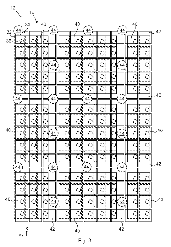
Fig. 3 schematically represents a partial top view of the radiation detector
12
in Figs. 1 and 2. In Fig. 3, the imaging pixels 30 and the readout pixels 32
are
square. The imaging pixels 30 are illustrated as squares with solid lines, the
readout pixels 32 are illustrated as squares with dashed lines, the
interconnections 36 are illustrated as circles with dashed lines, and the vias
44 are illustrated as circles with dashed lines.
As can be seen in Fig. 3, each readout pixel 32 has a first width in the first
direction (e.g. along the X-axis) that is smaller than a first width in the
first
direction of each imaging pixel 30 and each readout pixel 32 has a second
width in the second direction (e.g. along the Y-axis) that is smaller than a
second width in the second direction of each imaging pixel 30. In the example
in Fig. 3, it can be seen that the connection positions of the
interconnections
36 on the charge collection electrodes 28 are varied with respect to
neighboring charge collection electrodes 28. For example, the location of a
connection position of the interconnection 36 on the charge collection
electrodes 28 in an associated imaging pixel 30 in readout group 40 may be
CA 03095974 2020-10-02
WO 2019/219733
PCT/EP2019/062442
17
in a different X and/or Y location or offset relative to a neighboring charge
collection electrode 28 in the XY-plane. The neighboring charge collection
electrode can be defined as a charge collection electrode of an adjacent
imaging pixel 30 or a charge collection electrode of any other imaging pixel
30 in the specific readout group 40.
Fig. 3 further shows that the readout pixels 32 in each readout group 40 are
more compactly arranged in the first direction and in the second direction
than the associated imaging pixels 30 such that a plurality of streets 42 is
formed. Streets 42 are formed in both the first direction and in the second
direction between adjacent readout groups 40.
The streets 42 between readout groups 40 can define the readout pixels 32 in
one readout group 40 from the readout pixels 32 in and another adjacent
readout group 40. An edge (in the XY-plane) between an outer readout pixel
32 and a street 42 can define a boundary of a readout group 40. A readout
group first width in the first direction extends from a maximum distance
between two readout group boundaries in the first direction. A readout group
second width in the second direction extends from a maximum distance
between two readout group boundaries in the second direction.
An imaging group refers to the imaging pixels 30 associated with (or coupled
to) the readout pixel 32 in a readout group 40. The number of imaging pixels
in the imaging group can be the same number as the readout pixels 32 in
the readout group 40. An imaging group first width in the first direction
extends from a maximum distance between two imaging group boundaries in
the first direction. An imaging group second width in the second direction
25 extends from a maximum distance between two imaging group boundaries in
the second direction.
Similar to the readout pixels 32 and imaging pixels 30 described above, each
readout group 40 has an area in the XY-plane that is smaller than the area of
an associated imaging group in the XY-plane. For example, each readout
30 group 40 may have a width (or readout group first width) in a first
direction
CA 03095974 2020-10-02
WO 2019/219733
PCT/EP2019/062442
18
(e.g. along the X-axis) that is smaller than a width (or imaging group first
width) in the first direction of an associated imaging group and each readout
group 40 may have a width (or readout group second width) in a second
direction (e.g. along the Y-axis) that is smaller than a width (or imaging
group second width) in the second direction of the associated imaging group.
Alternatively, each readout group 40 may have a width (or readout group first
width) in a first direction (e.g. along the X-axis) that is smaller than a
width
(or imaging group first width) in the first direction of an associated imaging
group and each readout group 40 may have a width (or readout group second
width) in a second direction (e.g. along the Y-axis) that is equal to, or
substantially equal to, a width (or imaging group second width) in the second
direction of the associated imaging group.
Fig. 4 is a flowchart outlining the general steps of a method of manufacturing
a sensor unit 14 with a conversion element 22 connected to a readout
substrate 24. The method comprises a step Si of providing the conversion
element 22 comprising a plurality of imaging pixels 30, wherein each imaging
pixel 30 is configured to directly convert radiation into an electrical charge
and wherein each imaging pixel 30 comprises a charge collection electrode
28, wherein a plurality of outer edge imaging pixels of the conversion element
22 define boundaries of a conversion element effective area. The method
further comprises a step S2 of providing a readout substrate 24 comprising a
plurality of readout pixels 32, wherein a plurality of outer edge readout
pixels
of the readout substrate 24 define boundaries of a readout substrate effective
area. The method further comprises a step S3 of connecting each charge
collection electrode 28 of the imaging pixels 30 on a surface of the
conversion
element 22 to a readout electrode 34 of an associated readout pixel 32 on a
first surface of the readout substrate 24 by means of an interconnection 36 at
a connection position on the charge collection electrode 28, wherein the
conversion element effective area has a substantially same area as the
readout substrate effective area.
While the present disclosure has been described with reference to exemplary
embodiment, it will be appreciated that the present invention is not limited
to
CA 03095974 2020-10-02
WO 2019/219733
PCT/EP2019/062442
19
what has been described above. For example, it will be appreciated that the
dimensions of the parts may be varied as needed. Accordingly, it is intended
that the present invention may be limited only by the scope of the claims
appended hereto.