Note: Descriptions are shown in the official language in which they were submitted.
CA 03096346 2020-10-06
DESCRIPTION
TITLE OF INVENTION: ARRAY ANTENNA APPARATUS AND
COMMUNICATION DEVICE
TECHNICAL FIELD
[0001] The invention relates to an array antenna apparatus having a plurality
of
radiation conductors formed on a dielectric substrate, and a communication
device
including the array antenna apparatus.
BACKGROUND ART
[0002] The following Non-Patent Literature 1 discloses an array antenna having
an
array of patch antennas as radiation conductors.
In the array antenna having an array of patch antennas, the beam width of an
array element pattern in an E-plane which is an electric field plane of the
patch antennas
is narrower than the beam width of an array element pattern in an H-plane
which is a
magnetic field plane.
Therefore, when the array antenna whose main beam direction is an E-plane
direction performs wide-angle beam scanning, a beam scanning loss may
increase.
It is conceivable that one of the factors of increasing the beam scanning loss
is
that since the influence of surface waves is great in the E-plane direction of
the array
antenna, cross-coupling between the plurality of patch antennas increases.
[0003] The following Non-Patent Literature 1 describes that surface waves can
be
suppressed when a thickness h of a substrate having patch antennas formed on
its one
surface and having a ground plate formed on its other surface is a thickness
satisfying
the following expression (1):
1
Date Recue/Date Received 2020-10-06
CA 03096346 2020-10-06
0.3Ao
h < ( )
21T-rFr
In expression (1), X0 is free-space wavelength and Er is the dielectric
constant
of the substrate.
CITATION LIST
NON-PATENT LITERATURE
[0004] Non-Patent Literature 1: Ramesh Garg, Prakash Bhartia, Inder Bahl,
"Microstrip Antenna Design Handbook", Artech House Antennas and Propagation
Library, p. 46, 2000
SUMMARY OF INVENTION
TECHNICAL PROBLEM
[0005] The conventional array antenna can suppress surface waves when the
thickness
h of the substrate satisfies expression (1). However, the thickness h of the
substrate
also influences the frequency band of the antenna, and when the thickness h of
the
substrate is thin, the frequency band of the antenna is narrow.
To ensure a desired frequency band, the conventional array antenna may not be
able to ensure a thickness that satisfies expression (1) as the thickness h of
the substrate.
When the conventional array antenna cannot ensure a thickness that satisfies
expression (1) as the thickness h of the substrate, there is a problem that
surface waves
cannot be suppressed.
[0006] The invention is made to solve a problem such as that described above,
and an
object of the invention is to obtain an array antenna apparatus and a
communication
device that can suppress surface waves while ensuring a desired frequency
band.
2
Date Recue/Date Received 2020-10-06
CA 03096346 2020-10-06
SOLUTION TO PROBLEM
[0007] An array antenna apparatus according to the invention includes: a
dielectric
substrate; a plurality of radiation conductors formed on a first plane of the
dielectric
substrate; a first ground conductor formed on portions of the first plane of
the dielectric
substrate at locations that surround the plurality of radiation conductors and
that create
clearances between the plurality of radiation conductors; a second ground
conductor
formed on a portion of a second plane of the dielectric substrate at a
location opposite to
the first ground conductor; a plurality of connecting conductors each provided
inside the
dielectric substrate in such a manner that one end of the connecting conductor
is
connected to the first ground conductor and another end of the connecting
conductor is
connected to the second ground conductor, a location of the one end connected
to the
first ground conductor being a location that surrounds any one of the
plurality of
radiation conductors; a dielectric layer having one surface bonded to the
second plane of
the dielectric substrate and the second ground conductor; and a feeding
substrate having
one surface bonded to another surface of the dielectric layer, the feeding
substrate
electromagnetically coupling radio waves to the plurality of radiation
conductors
through the dielectric layer and the dielectric substrate.
ADVANTAGEOUS EFFECTS OF INVENTION
[0008] According to the invention, an array antenna apparatus is configured to
include
a plurality of connecting conductors each provided inside a dielectric
substrate in such a
manner that one end of the connecting conductor is connected to a first ground
conductor and another end of the connecting conductor is connected to a second
ground
conductor, a location of the one end connected to the first ground conductor
being a
3
Date Recue/Date Received 2020-10-06
CA 03096346 2020-10-06
location that surrounds any one of a plurality of radiation conductors.
Therefore, the
array antenna apparatus according to the invention can suppress surface waves
while
ensuring a desired frequency band.
BRIEF DESCRIPTION OF DRAWINGS
[0009] FIG. 1 is a plan view showing an array antenna apparatus of a first
embodiment.
FIG. 2 is a B-B' cross-sectional view of the array antenna apparatus shown in
FIG. 1.
FIG. 3 is a cross-sectional view showing the inside of a feeding substrate 8
of
the array antenna apparatus shown in FIG. 2.
FIG. 4 is a plan view showing a simulation-target array antenna apparatus.
FIG. 5 is an explanatory diagram showing simulation results for a radiation
pattern in an E-plane direction of the array antenna apparatus shown in FIG.
4.
FIG. 6 is a cross-sectional view showing an array antenna apparatus of a
second embodiment.
FIG. 7 is an explanatory diagram showing simulation results for array element
patterns of array antenna apparatuses.
FIG. 8 is an explanatory diagram showing reflectance properties of the array
antenna apparatuses.
FIG. 9 is a cross-sectional view showing an array antenna apparatus of a third
embodiment.
FIG. 10 is an explanatory diagram showing an arrangement of a plurality of
radiation conductors 2 on a first plane la of a dielectric substrate 1.
FIG. 11 is an explanatory diagram showing an arrangement of the plurality of
4
Date Recue/Date Received 2020-10-06
CA 03096346 2020-10-06
radiation conductors 2 on the first plane la of the dielectric substrate 1.
FIG. 12 is an explanatory diagram showing an arrangement of the plurality of
radiation conductors 2 on the first plane la of the dielectric substrate 1.
FIG. 13 is a configuration diagram showing a communication device of a sixth
embodiment.
DESCRIPTION OF EMBODIMENTS
[0010] To describe the invention in more detail, embodiments for carrying out
the
invention will be described below with reference to the accompanying drawings.
[0011] First Embodiment.
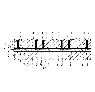
FIG. 1 is a plan view showing an array antenna apparatus of a first
embodiment.
FIG. 2 is a B-B' cross-sectional view of the array antenna apparatus shown in
FIG. 1.
In FIGS. 1 and 2, a dielectric substrate 1 is a substrate formed of a
dielectric.
Radiation conductors 2 each are a square patch element formed on a first plane
la of the dielectric substrate 1.
In the array antenna apparatus shown in FIG. 1, nine radiation conductors 2
(three radiation conductors 2 in an X-direction and three radiation conductors
2 in a Y-
direction) are formed on the first plane la of the dielectric substrate 1.
However, it is
sufficient that a plurality of radiation conductors 2 are formed on the first
plane la, and
two to eight radiation conductors 2 or ten or more radiation conductors 2 may
be
formed.
In the array antenna apparatus shown in FIG. 1, the radiation conductors 2
have
a square shape. However, the radiation conductors 2 may have any shape and may
Date Recue/Date Received 2020-10-06
CA 03096346 2020-10-06
have a triangle shape, a pentagon shape, a circle shape, or the like.
[0012] A first ground conductor 3 is a conductor grid formed on portions of
the first
plane la of the dielectric substrate 1 at locations that surround the
plurality of radiation
conductors 2 and that create clearances 4 between the plurality of radiation
conductors
2.
In the array antenna apparatus shown in FIG. 1, since the nine radiation
conductors 2 have a square shape, the first ground conductor 3 has a shape in
which
nine squares are cut out.
A second ground conductor 5 is a conductor grid formed on a portion of a
second plane lb of the dielectric substrate 1 at a location opposite to the
first ground
conductor 3.
The first ground conductor 3 and the second ground conductor 5 have the same
shape.
[0013] Connecting conductors 6 each are a through-hole via provided inside the
dielectric substrate 1 in such a manner that one end thereof is connected to
the first
ground conductor 3 and the other end thereof is connected to the second ground
conductor 5.
A location of the one end of the connecting conductor 6 connected to the first
ground conductor 3 is a location that surrounds any one of the plurality of
radiation
conductors 2.
In the array antenna apparatus shown in FIG. 1, 24 connecting conductors 6 are
connected at their one ends to the first ground conductor 3 per radiation
conductor 2 so
as to surround the radiation conductor 2.
[0014] A dielectric layer 7 is a layer having one surface 7a bonded to the
second plane
lb of the dielectric substrate 1 and the second ground conductor 5.
6
Date Recue/Date Received 2020-10-06
CA 03096346 2020-10-06
The dielectric layer 7 is a layer formed of a dielectric having the same
dielectric constant as that of the dielectric that forms the dielectric
substrate 1.
The dielectric layer 7 is not limited to a layer formed of a dielectric and
may
be, for example, a layer formed of a dielectric adhesive having the same
dielectric
constant as that of the dielectric that forms the dielectric substrate 1.
[0015] A feeding substrate 8 is a substrate that has one surface 8a bonded to
another
surface 7b of the dielectric layer 7 and that electromagnetically couples
radio waves to
the plurality of radiation conductors 2 through the dielectric layer 7 and the
dielectric
substrate 1.
The feeding substrate 8 includes a triplate line as a line for
electromagnetically
coupling radio waves to the respective plurality of radiation conductors 2.
An element occupation area 9 is an occupation area per radiation conductor 2,
and is determined by spacing in the X-direction between the radiation
conductors 2 and
spacing in the Y-direction between the radiation conductors 2.
Locations at which one ends of the plurality of connecting conductors 6
surround the radiation conductor 2 are inside the element occupation area 9.
[0016] FIG. 3 is a cross-sectional view showing the inside of the feeding
substrate 8 of
the array antenna apparatus shown in FIG. 2.
In FIG. 3, a ground conductor 11 is formed on the one surface 8a of the
feeding
substrate 8.
A ground conductor 12 is formed on another surface 8b of the feeding substrate
8.
A central conductor 13 is a conductor formed between the ground conductor 11
and the ground conductor 12.
Connecting conductors 14 each are provided inside the feeding substrate 8 in
7
Date Recue/Date Received 2020-10-06
CA 03096346 2020-10-06
such a manner that one end thereof is connected to the ground conductor 11 and
the
other end thereof is connected to the ground conductor 12.
Connecting conductors 15 each have one end connected to the central
conductor 13 and the other end coming out of the feeding substrate 8.
Coupling slots 16 each are an opening made in the ground conductor 11 to
electromagnetically couple a corresponding one of the plurality of radiation
conductors
2 to a radio wave.
Each of the ground conductor 11, the ground conductor 12, the central
conductor 13, the connecting conductors 14, the connecting conductors 15, and
the
coupling slots 16 is an element of the triplate line included in the feeding
substrate 8.
[0017] Next, the operation will be described.
In the feeding substrate 8, since the coupling slots 16 are made in the ground
conductor 11, when electrical signals are fed to the connecting conductors 15
from an
external source, radio waves are electromagnetically coupled to the plurality
of radiation
conductors 2 through the dielectric layer 7 and the dielectric substrate 1.
The radio waves coupled to the plurality of radiation conductors 2 are
radiated
into space.
Note, however, that a part of the radio waves coupled to the plurality of
radiation conductors 2 becomes surface-wave components that propagate through
the
dielectric substrate 1.
[0018] When the plurality of connecting conductors 6 are not arranged so as to
surround the radiation conductors 2, a surface-wave component which is a part
of a
radio wave coupled to a given radiation conductor 2 propagates to another
radiation
conductor 2 adjacent to the given radiation conductor 2.
By the surface-wave component propagating to another radiation conductor 2,
8
Date Recue/Date Received 2020-10-06
CA 03096346 2020-10-06
cross-coupling between the plurality of radiation conductors 2 increases,
increasing a
beam scanning loss of the array antenna apparatus.
In the array antenna apparatus shown in FIG. 1, since the plurality of
connecting conductors 6 are arranged so as to surround the radiation
conductors 2, a
surface-wave component from a radiation conductor 2 surrounded by the
plurality of
connecting conductors 6 is shielded by the plurality of connecting conductors
6, the first
ground conductor 3, and the second ground conductor 5.
Therefore, the array antenna apparatus shown in FIG. 1 suppresses an increase
in cross-coupling between the plurality of radiation conductors 2, and thus
can suppress
a reduction in gain in a wide-angle direction of an array element pattern.
[0019] In addition, in the array antenna apparatus shown in FIG. 1, since
surface-wave
components from the radiation conductors 2 are shielded by the plurality of
connecting
conductors 6, the first ground conductor 3, and the second ground conductor 5,
a
thickness h of the dielectric substrate 1 does not need to be a thickness
satisfying
expression (1). Namely, in the array antenna apparatus shown in FIG. 1, even
if the
thickness h of the dielectric substrate 1 is thicker than (0.3X0)/(27CVEr),
surface-wave
components from the radiation conductors 2 can be shielded.
Hence, in the array antenna apparatus shown in FIG. 1, since the thickness h
of
the dielectric substrate 1 can be made thicker than (0.3Xo)/(27c gcr), the
frequency band
of the antenna can be widened.
[0020] When an array antenna apparatus does not include the plurality of
connecting
conductors 6, the first ground conductor 3, and the second ground conductor 5,
a
radiation region of a main radiation component, which is a radio wave radiated
into
space, per radiation conductor 2 corresponds to a region of the element
occupation area
9 excluding the radiation conductor 2.
9
Date Recue/Date Received 2020-10-06
CA 03096346 2020-10-06
The array antenna apparatus shown in FIG. 1 includes the plurality of
connecting conductors 6, the first ground conductor 3, and the second ground
conductor
5, and thus, a radiation region of a main radiation component per radiation
conductor 2
corresponds to a portion of a region surrounded by the plurality of connecting
conductors 6 excluding the radiation conductor 2.
Therefore, the array antenna apparatus shown in FIG. 1 has a smaller radiation
region of a main radiation component than that of the array antenna apparatus
that does
not include the plurality of connecting conductors 6, the first ground
conductor 3, and
the second ground conductor 5, and thus can widen the beam width of an array
element
pattern.
[0021] Here, there is an array antenna apparatus with a cavity structure that
includes a
dielectric substrate having a plurality of radiation conductors formed on a
first plane and
having a ground plate formed on a second plane; and a feeding substrate
grounded to
the ground plate.
In the array antenna apparatus with a cavity structure, upon multi-layering
the
dielectric substrate and the feeding substrate, the dielectric substrate and
the feeding
substrate are often fixed by screwing. When the dielectric substrate and the
feeding
substrate are fixed by screwing, a misalignment, etc., may occur between the
dielectric
substrate and the feeding substrate, by which electrical characteristics of
the antenna
may change from designed values.
The array antenna apparatus shown in FIG. 1 has a structure in which the
feeding substrate 8 is bonded to the dielectric substrate 1 through the
dielectric layer 7
therebetween, and the feeding substrate 8 does not need to be grounded to the
second
ground conductor 5.
Therefore, in the structure of the array antenna apparatus shown in FIG. 1, it
is
Date Recue/Date Received 2020-10-06
CA 03096346 2020-10-06
sufficient multi-layering the dielectric substrate 1 and the feeding substrate
8 through
the dielectric layer 7 therebetween, and compared to the cavity structure,
multi-layering
of the dielectric substrate 1 and the feeding substrate 8 is easy. Thus, a
misalignment,
etc., are less likely to occur between the dielectric substrate 1 and the
feeding substrate
8, reducing the possibility that electrical characteristics of the antenna
change from
designed values.
[0022] The fact that the array antenna apparatus of the first embodiment can
achieve
wide coverage by widening the beam width of an array element pattern will be
described below.
FIG. 4 is a plan view showing a simulation-target array antenna apparatus, and
in FIG. 4, the same reference signs as those in FIG. 1 indicate the same or
corresponding portions.
In the array antenna apparatus shown in FIG. 4, 32 radiation conductors 2
(eight radiation conductors 2 in the X-direction and four radiation conductors
2 in the Y-
direction) are formed on the first plane la of the dielectric substrate 1.
FIG. 5 is an explanatory diagram showing simulation results for a radiation
pattern (array element pattern) in an E-plane direction of the array antenna
apparatus
shown in FIG. 4.
FIG. 5 also shows simulation results for an array element pattern of a
comparison-target array antenna apparatus, in addition to the array antenna
apparatus
shown in FIG. 4 which is the array antenna apparatus of the first embodiment.
In the comparison-target array antenna apparatus, too, 32 radiation conductors
2 (eight radiation conductors 2 in the X-direction and four radiation
conductors 2 in the
Y-direction) are formed on the first plane la of the dielectric substrate 1,
but the
comparison-target array antenna apparatus does not include the connecting
conductors
11
Date Recue/Date Received 2020-10-06
CA 03096346 2020-10-06
6, the first ground conductor 3, and the second ground conductor 5.
[0023] In simulation, any one of the 32 radiation conductors 2 is selected in
turn, and
an array element pattern at a time when each of the selected radiation
conductors 2 is
excited is computed. Then, in the simulation, an average value of the computed
32
array element patterns is calculated.
In the simulation, upon exciting any one of the radiation conductors 2, the
other
31 radiation conductors 2 are matched and terminated.
In addition, in the simulation, the spacing between the 32 radiation
conductors
2 is 0.54 free-space wavelength.
In FIG. 5, a horizontal axis represents angle and a vertical axis represents
gain
normalized with gain in a 0-degree front direction.
Reference sign 21 indicates simulation results for an array element pattern of
the array antenna apparatus shown in FIG. 4, and reference sign 22 indicates
simulation
results for an array element pattern of the comparison-target array antenna
apparatus.
[0024] When the beam width of an array element pattern is -60 to +60 degrees,
the
beam width of the array element pattern is generally said to be wide.
In addition, when the gain of an array element pattern is roughly greater than
-3
dB, the gain is generally said to be large.
When the simulation results 21 are compared with the simulation results 22, at
a beam width of -60 to +60 degrees, the gain of the array element pattern
indicated by
the simulation results 21 is larger than the gain of the array element pattern
indicated by
the simulation results 22.
In addition, in the simulation results 21, the gain of the array element
pattern is
roughly greater than -3 dB at a beam width of -60 to +60 degrees.
Therefore, it can be seen that compared to the comparison-target array antenna
12
Date Recue/Date Received 2020-10-06
CA 03096346 2020-10-06
apparatus, in the array antenna apparatus shown in FIG. 4, the beam width of
the array
element pattern is widened, and wide coverage can be achieved.
[0025] In the above-described first embodiment, an array antenna apparatus is
configured to include the plurality of connecting conductors 6 each provided
inside the
dielectric substrate 1 in such a manner that one end thereof is connected to
the first
ground conductor 3 and the other end thereof is connected to the second ground
conductor 5, and a location of the one end connected to the first ground
conductor 3
being a location that surrounds any one of the plurality of radiation
conductors 2.
Therefore, the array antenna apparatus can suppress surface waves while
ensuring a
desired frequency band.
[0026] The feeding substrate 8 shown in FIG. 3 includes the triplate line for
electromagnetically coupling radio waves to the respective plurality of
radiation
conductors 2. However, a line for electromagnetically coupling radio waves is
not
limited to the triplate line.
Therefore, the feeding substrate 8 may have, for example, a ground conductor
formed on the other surface 8b and a microstrip line formed on the one surface
8a, as a
line for electromagnetically coupling radio waves to the respective plurality
of radiation
conductors 2.
[0027] Second Embodiment.
The array antenna apparatus of the first embodiment shows an array antenna
apparatus in which the dielectric substrate 1 is a single-layer substrate.
A second embodiment describes an array antenna apparatus in which the
dielectric substrate 1 is a multi-layer substrate having a plurality of
dielectric substrates
stacked on top of each other.
[0028] FIG. 6 is a cross-sectional view showing an array antenna apparatus of
the
13
Date Regue/Date Received 2020-10-06
CA 03096346 2020-10-06
second embodiment.
A plan view of the array antenna apparatus of the second embodiment is the
same as that of FIG. 1, and FIG. 6 shows a B-B' cross section of the array
antenna
apparatus shown in FIG. 1.
In FIG. 6, the same reference signs as those in FIGS. 1 to 3 indicate the same
or corresponding portions and thus description thereof is omitted.
A dielectric substrate 1 is a multi-layer substrate including a dielectric
substrate
31, a dielectric layer 32, and a dielectric substrate 33.
The dielectric substrate 31, the dielectric layer 32, and the dielectric
substrate
33 have the same dielectric constant.
The dielectric layer 32 is a layer inserted between the dielectric substrate
31
and the dielectric substrate 33, and is formed of a dielectric.
Note, however, that the dielectric layer 32 is not limited to a layer formed
of a
dielectric and may be, for example, a layer formed of a dielectric adhesive.
The array antenna apparatus shown in FIG. 6 shows an array antenna apparatus
in which the dielectric substrate 1 is a multi-layer substrate having three
layers.
However, the dielectric substrate 1 is not limited to a multi-layer substrate
having three
layers, and may be a multi-layer substrate having two layers or four or more
layers.
[0029] When the dielectric substrate 1 is a single-layer substrate, the
thickness of the
dielectric substrate 1 has an upper limit and the dielectric substrate 1 may
not be able to
ensure a desired thickness.
In the array antenna apparatus shown in FIG. 6, since the dielectric substrate
1
is a multi-layer substrate, by increasing the number of stacked layers of the
multi-layer
substrate, the thickness of the dielectric substrate 1 can be made thicker
than the
thickness of a single-layer substrate.
14
Date Recue/Date Received 2020-10-06
CA 03096346 2020-10-06
Therefore, by increasing the thickness of the dielectric substrate 1, the
array
antenna apparatus shown in FIG. 6 can further widen the frequency band than
the array
antenna apparatus of the first embodiment.
[0030] FIG. 7 is an explanatory diagram showing simulation results for array
element
patterns of array antenna apparatuses.
FIG. 7 shows simulation results for an array element pattern obtained when the
dielectric substrate 1 is a single-layer substrate, and simulation results for
an array
element pattern obtained when the dielectric substrate 1 is a multi-layer
substrate.
An array antenna apparatus with the dielectric substrate 1 being a single-
layer
substrate is the array antenna apparatus of the first embodiment, and an array
antenna
apparatus with the dielectric substrate 1 being a multi-layer substrate is the
array
antenna apparatus of the second embodiment.
It is assumed that in both array antenna apparatuses, as shown in FIG. 4, 32
radiation conductors 2 are formed.
[0031] In simulation, any one of the 32 radiation conductors 2 is selected in
turn, and
an array element pattern at a time when each of the selected radiation
conductors 2 is
excited is computed. Then, in the simulation, an average value of the computed
32
array element patterns is calculated.
In the simulation, it is assumed that, upon exciting any one of the radiation
conductors 2, the other 31 radiation conductors 2 are matched and terminated.
In addition, in the simulation, the spacing between the 32 radiation
conductors
2 is 0.54 free-space wavelength.
In FIG. 7, a horizontal axis represents angle and a vertical axis represents
gain
normalized with gain in a 0-degree front direction.
Reference sign 23 indicates simulation results for an array element pattern
Date Recue/Date Received 2020-10-06
CA 03096346 2020-10-06
obtained when the dielectric substrate 1 is a single-layer substrate, and
reference sign 24
indicates simulation results for an array element pattern obtained when the
dielectric
substrate 1 is a multi-layer substrate.
The simulation results 23 and the simulation results 24 are substantially the
same.
Therefore, it can be seen that in the array antenna apparatus whose dielectric
substrate 1 is a multi-layer substrate, too, the beam width of the array
element pattern is
further widened and wider coverage can be achieved over the comparison-target
array
antenna apparatus shown in the first embodiment.
[0032] FIG. 8 is an explanatory diagram showing reflectance properties of the
array
antenna apparatuses.
In FIG. 8, a horizontal axis represents frequency normalized with a center
frequency fo of a frequency band, and a vertical axis represents the
reflection coefficient
of the antenna. Reflection coefficients shown in FIG. 8 are also obtained by
simulation.
Reference sign 25 indicates the reflection coefficient of the antenna obtained
when the dielectric substrate 1 is a single-layer substrate, and reference
sign 26 indicates
the reflection coefficient of the antenna obtained when the dielectric
substrate 1 is a
multi-layer substrate.
As is clear by comparing the reflection coefficient 25 with the reflection
coefficient 26, it can be seen that the array antenna apparatus whose
dielectric substrate
1 is a multi-layer substrate obtains a lower reflection characteristic over
the low to high
frequency sides of the frequency band than that of the array antenna apparatus
whose
dielectric substrate 1 is a single-layer substrate.
[0033] In the above-described second embodiment, the array antenna apparatus
is
16
Date Recue/Date Received 2020-10-06
CA 03096346 2020-10-06
configured in such a manner that the dielectric substrate 1 is a multi-layer
substrate
having a plurality of dielectric substrates stacked on top of each other.
Therefore, the
array antenna apparatus can obtain a lower reflection characteristic over a
wide
frequency band than an array antenna apparatus whose dielectric substrate 1 is
a single-
layer substrate.
[0034] Third Embodiment.
In the array antenna apparatus of the first embodiment, the radiation
conductors
2 are formed on the first plane la of the dielectric substrate 1.
A third embodiment describes an array antenna apparatus in which second
radiation conductors 30 are also formed in the middle of a dielectric
substrate 1 which is
a multi-layer substrate, in addition to the radiation conductors 2 formed on
the first
plane la of the dielectric substrate 1.
[0035] FIG. 9 is a cross-sectional view showing the array antenna apparatus of
the
third embodiment.
A plan view of the array antenna apparatus of the third embodiment is the same
as that of FIG. 1, and FIG. 9 shows a B-B' cross section of the array antenna
apparatus
shown in FIG. 1.
In FIG. 9, the same reference signs as those in FIGS. 1 to 3 and 6 indicate
the
same or corresponding portions and thus description thereof is omitted.
The radiation conductors 2 shown in FIG. 9 are first radiation conductors.
The plurality of second radiation conductors 30 are formed at locations on the
dielectric substrate 33 included in the dielectric substrate 1 that are
opposite to the
respective plurality of first radiation conductors 2.
In the array antenna apparatus shown in FIG. 9, the second radiation
conductors 30 are formed on the dielectric substrate 33. However, the second
radiation
17
Date Recue/Date Received 2020-10-06
CA 03096346 2020-10-06
conductors 30 are not limited to being formed on the dielectric substrate 33.
Therefore, the second radiation conductors 30 may be formed on, for example, a
plane
of the dielectric substrate 31 on a dielectric layer 32 side.
[0036] In the array antenna apparatus shown in FIG. 9, the first radiation
conductors 2
and the second radiation conductors 30 are stacked on top of each other.
For example, when the second radiation conductors 30 different in thickness
than the first radiation conductors 2 are formed on the dielectric substrate
33, the array
antenna apparatus shown in FIG. 9 causes multiple resonance in which the
resonant
frequency of the first radiation conductors 2 and the resonant frequency of
the second
radiation conductors 30 differ from each other.
An array antenna apparatus that causes multiple resonance does not have the
second radiation conductors 30 formed therein, and thus can achieve wide
coverage
compared to an array antenna apparatus that does not cause multiple resonance.
Here, the second radiation conductors 30 different in thickness than the first
radiation conductors 2 are formed on the dielectric substrate 33. An array
antenna
apparatus in which the second radiation conductors 30 different in shape than
the first
radiation conductors 2 are formed on the dielectric substrate 33 also causes
multiple
resonance.
[0037] Fourth Embodiment.
A fourth embodiment describes an array antenna apparatus in which a thickness
h7 of the dielectric layer 7 is a thickness satisfying the following
expression (2):
0.32.0
h7 - ( 2 )
In expression (2), X0 is free-space wavelength and Er is the dielectric
constant
of the dielectric layer 7.
18
Date Recue/Date Received 2020-10-06
CA 03096346 2020-10-06
[0038] Across-sectional view of the array antenna apparatus of the fourth
embodiment
is any one of FIGS. 2, 3, 6, and 9.
In the array antenna apparatus of the fourth embodiment, surface-wave
components from the radiation conductors 2 are shielded by the plurality of
connecting
conductors 6, the first ground conductor 3, and the second ground conductor 5.
The array antenna apparatus of the fourth embodiment further suppresses
surface-wave components from the radiation conductors 2 by setting the
thickness h7 of
the dielectric layer 7 to be a thickness satisfying expression (2).
When the thickness h7 of the dielectric layer 7 is a thickness satisfying
expression (2), since the thickness h7 of the dielectric layer 7 is
sufficiently thin, a
propagation path of a surface-wave component between adjacent radiation
conductors 2
can be considered to be electrically substantially shielded.
Therefore, the influence of cross-coupling between the adjacent radiation
conductors 2 can be further reduced.
[0039] In the above-described fourth embodiment, an array antenna apparatus is
configured in such a manner that the thickness h7 of the dielectric layer 7 is
a thickness
satisfying expression (2). Therefore, the array antenna apparatus further
suppresses
surface waves and can widen an array element pattern over the array antenna
apparatus
of the first embodiment.
[0040] Fifth Embodiment.
In the array antenna apparatus of the first embodiment, an arrangement of the
plurality of radiation conductors 2 on the first plane la of the dielectric
substrate 1 is a
square arrangement.
However, this is merely an example and the array antenna apparatus may be
configured in such a manner that, as shown in FIG. 10, an arrangement of the
plurality
19
Date Recue/Date Received 2020-10-06
CA 03096346 2020-10-06
of radiation conductors 2 on the first plane la of the dielectric substrate 1
is a linear
arrangement, and can obtain the same advantageous effect as that of the array
antenna
apparatus of the first embodiment.
In addition, the array antenna apparatus may be configured in such a manner
that, as shown in FIG. 11, an arrangement of the plurality of radiation
conductors 2 on
the first plane la of the dielectric substrate 1 is a triangular arrangement,
and can obtain
the same advantageous effect as that of the array antenna apparatus of the
first
embodiment.
In addition, the array antenna apparatus may be configured in such a manner
that, as shown in FIG. 12, an arrangement of the plurality of radiation
conductors 2 on
the first plane la of the dielectric substrate 1 is a non-periodic
arrangement, and can
obtain the same advantageous effect as that of the array antenna apparatus of
the first
embodiment.
FIGS. 10 to 12 are explanatory diagrams showing arrangements of the plurality
of radiation conductors 2 on the first plane la of the dielectric substrate 1.
[0041] Sixth Embodiment.
A sixth embodiment describes a communication device having any one of the
array antenna apparatuses of the first to fifth embodiments mounted thereon.
FIG. 13 is a configuration diagram showing a communication device of the
sixth embodiment.
In FIG. 13, an array antenna apparatus 41 is an array antenna apparatus that
transmits and receives radio waves, and is any one of the array antenna
apparatuses of
the first to fifth embodiments.
A communication unit 42 is connected to the connecting conductors 15 of the
array antenna apparatus 41.
Date Recue/Date Received 2020-10-06
CA 03096346 2020-10-06
The communication unit 42 outputs, as an electrical signal corresponding to a
transmission-target radio wave, for example, an electrical signal which is
modulated by
a modulator installed therein to the connecting conductors 15 of the array
antenna
apparatus 41.
In addition, the communication unit 42 collects electrical signals
corresponding
to radio waves received by the array antenna apparatus 41, from the connecting
conductors 15 of the array antenna apparatus 41.
[0042] The communication device may be a mobile communication device or a
fixed
communication device.
The communication device can perform wireless communication with other
communication devices by mounting the array antenna apparatus 41 and the
communication unit 42 thereon.
The sixth embodiment shows the communication device including the array
antenna apparatus 41. However, it is not limited thereto, and a radar
apparatus
including the array antenna apparatus 41 may be adopted.
[0043] Note that in the invention of this application, a free combination of
the
embodiments, modifications to any component of the embodiments, or omissions
of any
component in the embodiments are possible within the scope of the invention.
INDUSTRIAL APPLICABILITY
[0044] The invention is suitable for an array antenna apparatus having a
plurality of
radiation conductors formed on a dielectric substrate.
The invention is suitable for a communication device including the array
antenna apparatus.
21
Date Recue/Date Received 2020-10-06
CA 03096346 2020-10-06
REFERENCE SIGNS LIST
[0045] 1: dielectric substrate, la: first plane, lb: second plane, 2:
radiation conductor
(first radiation conductor), 3: first ground conductor, 4: clearance, 5:
second ground
conductor, 6: connecting conductor, 7: dielectric layer, 7a: one surface, 7b:
other
surface, 8: feeding substrate, 8a: one surface, 8b: other surface, 9: element
occupation
area, 11, 12: ground conductor, 13: central conductor, 14, 15: connecting
conductor, 16:
coupling slot, 21 to 24: simulation results, 25, 26: reflection coefficient,
30: second
radiation conductor, 31: dielectric substrate, 32: dielectric layer, 33:
dielectric substrate
33, 41: array antenna apparatus, 42: communication unit
22
Date Recue/Date Received 2020-10-06