Note: Descriptions are shown in the official language in which they were submitted.
CA 03096824 2020-10-09
WO 2019/221784
PCT/US2018/062777
NON-INVASIVE WEARABLE BRAIN INTERFACE SYSTEMS
RELATED APPLICATIONS
[0001] The present application claims priority to PCT International
Application No.
PCT/US18/58580, filed October 31, 2018, which claims priority to U.S. Patent
Application No. 16/051,462, filed July 31, 2018, which claims priority under
35 U.S.C.
119(e) to U.S. Provisional Patent Application No. 62/673,065, filed on May 17,
2018,
and to U.S. Provisional Patent Application No. 62/687,659, filed on June 20,
2018.
These applications are incorporated herein by reference in their respective
entireties.
BACKGROUND INFORMATION
[0002] Detecting neural activity in the brain is useful for medical
diagnostics,
imaging, neuroengineering, brain-computer interfacing, and a variety of other
diagnostic
and consumer-related applications. For example, it may be desirable to detect
neural
activity in the brain of a patient to determine if a particular region of the
brain has been
impacted by reduced blood irrigation, a hemorrhage, or any other type of
damage. As
another example, it may be desirable to detect neural activity in the brain of
a user and
computationally decode the detected neural activity into commands that can be
used to
control various types of consumer electronics (e.g., by controlling a cursor
on a
computer screen, changing channels on a television, turning lights on, etc.).
[0003] A photodetector capable of detecting a single photon (i.e., a
single particle of
optical energy) is an example of a non-invasive detector that can be used to
detect
neural activity within the brain. For example, an array of these sensitive
photodetectors
can record photons that reflect off of tissue within the brain in response to
application of
one or more light pulses. Based on the time it takes for the photons to be
detected by
the photodetectors, neural activity and other attributes of the brain can be
determined
or inferred.
[0004] A photodetector that employs a semiconductor-based single-photon
avalanche diode (SPAD) is capable of capturing individual photons with very
high time-
of-arrival resolution (a few tens of picoseconds). When photons are absorbed
by a
SPAD, their energy frees bound charge carriers (electrons and holes) that then
become
free-carrier pairs. In the presence of an electric field created by a reverse
bias voltage
1
CA 03096824 2020-10-09
WO 2019/221784
PCT/US2018/062777
applied to the diode, these free-carriers are accelerated through a region of
the SPAD
referred to as the multiplication region. As the free carriers travel through
the
multiplication region, they collide with other carriers bound in the atomic
lattice of the
semiconductor, thereby generating more free carriers through a process called
impact
ionization. These new free-carriers also become accelerated by the applied
electric field
and generate yet more free-carriers. This avalanche event can be detected and
used to
determine an arrival time of the photon.
[0005] In order to enable detection of a single photon, a SPAD is biased
with a
reverse bias voltage having a magnitude greater than the magnitude of its
breakdown
voltage, which is the bias level above which free-carrier generation can
become self-
sustaining and result in a runaway avalanche. This biasing of the SPAD is
referred to
as arming the device. When the SPAD is armed, a single free carrier pair
created by
the absorption of a single photon can create a runaway avalanche resulting in
an easily
detectable macroscopic current.
[0006] Conventional SPAD architectures gate a SPAD (i.e., arm and disarm
the
SPAD) by selectively biasing the SPAD with a gating signal generated by an
active
voltage source. Use of an active voltage source to gate a SPAD may
disadvantageously introduce noise into the photodetector output, consume a
relatively
high amount of power, introduce supply voltage ripple within neighboring SPAD
architectures, and cause other undesirable effects.
BRIEF DESCRIPTION OF THE DRAWINGS
[0007] The accompanying drawings illustrate various embodiments and are
a part of
the specification. The illustrated embodiments are merely examples and do not
limit the
scope of the disclosure. Throughout the drawings, identical or similar
reference
numbers designate identical or similar elements.
[0008] FIG. 1 shows a conventional SPAD architecture known in the art.
[0009] FIG. 2 illustrates various components included in an exemplary
fast-gated
photodetector according to principles described herein.
[0010] FIG. 3A illustrates an exemplary photodetector system according
to principles
described herein.
[0011] FIG. 3B shows an exemplary non-invasive wearable brain interface
system
that implements photodetector system according to principles described herein.
2
CA 03096824 2020-10-09
WO 2019/221784
PCT/US2018/062777
[0012] FIG. 4A shows an exemplary SPAD circuit that may be used in the
photodetector architectures described herein.
[0013] FIG. 4B shows another exemplary SPAD circuit that may be used in
the
photodetector architectures described herein.
[0014] FIG. 5 is a flowchart that illustrates an exemplary mode of
operation of the
SPAD circuit of FIG. 4A according to principles described herein.
[0015] FIGS. 6-7 show exemplary switch states of the SPAD circuit of
FIG. 4A.
[0016] FIG. 8 shows an exemplary timing diagram that illustrates a
relationship
between the occurrence of a light pulse and a programmable gate delay
according to
principles described herein.
[0017] FIGS. 9A-9F show various circuits that may implement any of the
switches
described herein.
[0018] FIG. 10A illustrates an exemplary implementation of an inverter
according to
principles described herein.
[0019] FIG. 10B illustrates an exemplary implementation of a comparator
according
to principles described herein.
[0020] FIG. 11A shows another exemplary SPAD circuit that may be used in
the
photodetector architectures described herein.
[0021] FIG. 11B shows another exemplary SPAD circuit that may be used in
the
.. photodetector architectures described herein.
[0022] FIG. 12 is a flowchart that illustrates an exemplary mode of
operation of the
SPAD circuit of FIG. 11A according to principles described herein.
[0023] FIGS. 13-14 show exemplary switch states of the SPAD circuit of
FIG. 11A.
[0024] FIGS. 15-20 show alternative circuit topologies of the SPAD
circuit of FIG.
11A.
[0025] FIG. 21 illustrates an exemplary method according to principles
described
herein.
[0026] FIG. 22 illustrates another exemplary method according to
principles
described herein.
[0027] FIGS. 23-29 illustrate exemplary non-invasive wearable brain
interface
systems according to principles described herein.
3
CA 03096824 2020-10-09
WO 2019/221784
PCT/US2018/062777
DETAILED DESCRIPTION
[0028] Non-invasive wearable brain interface systems are described
herein. For
example, an exemplary non-invasive wearable brain interface system includes a
headgear configured to be worn on a head of the user and a plurality of self-
contained
photodetector units configured to removably attach to the headgear (e.g., by
fitting
within cutouts included in the headgear, attaching to protrusions or embedded
housings
of the headgear, or in any other suitable manner). The photodetector units
each include
a plurality of photodetectors configured to detect photons of light after the
photons
reflect from a target within a brain of the user. The brain interface system
further
includes a master control unit communicatively coupled to each of the
photodetector
units by way of a plurality of wires and configured to control the
photodetector units, the
master control unit comprising an input power port configured to connect to a
power
cable that provides power from a power source for the master control unit and
the
photodetector units.
[0029] Another exemplary non-invasive wearable brain interface system
includes a
headgear configured to be worn on a head of the user and a plurality of self-
contained
photodetector units configured to removably attach to the headgear. The
photodetector
units each include a plurality of photodetectors configured to detect photons
of light
.. after the photons reflect from a target within a brain of the user. A
photodetector
included in the plurality of photodetectors includes a SPAD and a capacitor.
The
capacitor is configured to be charged, while the SPAD is in a disarmed state,
with a
bias voltage by a voltage source. The capacitor is further configured to
supply, when
the SPAD is put in an armed state, the bias voltage to an output node of the
SPAD
such that a voltage across the SPAD is greater than a breakdown voltage of the
SPAD.
[0030] Another exemplary non-invasive wearable brain interface system
includes a
headgear configured to be worn on a head of the user and a plurality of self-
contained
photodetector units configured to removably attach to the headgear and fit
within
cutouts included in the headgear. The photodetector units each include a light
source
.. configured to generate light and a plurality of photodetectors configured
to detect
photons of the light after the photons reflect from a target within a brain of
the user. The
brain interface system further includes a master control unit communicatively
coupled to
each of the photodetector units by way of a plurality of wires and configured
to control
the photodetector units. The brain interface system further includes a power
source
4
CA 03096824 2020-10-09
WO 2019/221784
PCT/US2018/062777
configured to be worn off the head of the user, be connected to the master
control unit
by way of a power cable, and provide power for the master control unit and the
photodetector units.
[0031] The non-invasive wearable brain interface systems described
herein provide
various benefits and advantages over conventional brain interface systems. For
example, the non-invasive wearable brain interface systems may be effective in
detecting neural activity in the brain of a user while at the same time being
convenient
and relatively comfortable to wear by the user. For example, the user may wear
the
non-invasive wearable brain interface systems described herein while the user
performs daily activities, such as walking, exercising, working, etc. The non-
invasive
wearable brain interface systems described herein may also provide various
benefits
described in connection with the fast-gated photodetector architectures
described
herein and provide "real time" neural measurements.
[0032] Fast-gated photodetector architectures are also described herein.
The
photodetector architectures described herein may be implemented by the non-
invasive
wearable brain interface systems described herein and can be used to fast gate
a
SPAD while minimizing dead time, afterpulsing, power consumption, and time
jitter. The
photodetector architectures described herein can therefore increase signal-to-
noise
ratio of photodetection, thereby improving spatial and temporal resolution
compared to
conventional photodetectors. These and other advantages of the photodetector
architectures described herein will be described in more detail below.
[0033] FIG. 1 shows a conventional SPAD architecture known in the art
that may be
used in a conventional photodetector. In FIG. 1, a gating signal generated by
a voltage
source VGATE is applied to an output node of a SPAD. The gating signal
switches
between ground and an excess bias voltage. When the gating signal is equal to
ground,
the voltage across the SPAD is less than or equal to a breakdown voltage of
the SPAD,
which means that the SPAD is in a disarmed or "off" state in which the SPAD
cannot
avalanche. When the gating signal is equal to the excess bias voltage, the
voltage
across the SPAD is greater than the breakdown voltage of the SPAD, which means
that
the SPAD is in an armed or "on" state in which a photon can initiate a
detectable
avalanche within the SPAD.
[0034] While the SPAD is in the armed state, a photon incident upon the
SPAD may
initiate an avalanche within the SPAD. When the avalanche occurs, current
starts
flowing through capacitor CP and resistors RB and RT, which increases the
voltage at
5
CA 03096824 2020-10-09
WO 2019/221784
PCT/US2018/062777
the SPAD anode. This, in turn, reduces the voltage across the SPAD. When the
voltage
across the SPAD decreases below the breakdown voltage of the SPAD, the
avalanche
stops. This process is called passive quenching.
[0035] A number of disadvantages are associated with the conventional
SPAD
architecture shown in FIG. 1. For example, because the gating of the SPAD is
performed directly by the voltage source VGATE, the time it takes to arm the
SPAD is not
instantaneous. Rather, the time it takes to arm the SPAD depends on the rise
time of
the gating signal supplied by the voltage source VGATE (i.e., the time it
takes for the
gating signal to go from ground to the excess bias voltage). If a photon hits
the SPAD
during the rise time phase of the gating signal, the SPAD may not yet be armed
and
therefore may not detect the photon. Hence, any data collected by the
photodetector
during the rise time of the gating signal is corrupted and must be discarded.
[0036] Moreover, the passive quenching performed by the conventional
SPAD
architecture shown in FIG. 1 is a relatively slow process. Because the output
node of
the SPAD remains connected to the voltage source VGATE while SPAD is being
passively quenched, a relatively large amount of current (and hence, power) is
consumed by the SPAD architecture before the avalanche is passively quenched.
A
relatively slow passive quenching process may also lead to a high number of
traps in
the SPAD and high afterpulsing.
[0037] Another disadvantage of the conventional SPAD architecture of FIG. 1
is
unwanted supply voltage ripple across a photodetector array. For example, each
photodetector in an array of photodetectors may include the conventional SPAD
architecture of FIG. 1. In this configuration, when an avalanche happens
within a
particular SPAD, a large current flow from the SPAD's voltage source (e.g.,
VGATE) to
the SPAD may cause voltage variations on the voltages seen by other SPADs in
the
photodetector array. These voltage variations are exasperated as the number of
SPADs increase in a given photodetector array, and may cause variation in the
SPAD
parameters (e.g., probability of detecting a photon, dark current, timing,
etc.).
[0038] In contrast, the SPADs in the photodetector architectures
described herein
are not gated directly by an active voltage source, such as voltage source
VGATE.
Rather, an exemplary SPAD as described herein is gated with a capacitor that
is pre-
charged with a bias voltage before a command is provided to arm the SPAD.
Gating the
SPAD with a capacitor instead of with an active voltage source has a number of
advantages and benefits.
6
CA 03096824 2020-10-09
WO 2019/221784
PCT/US2018/062777
[0039] For example, a SPAD that is gated with a capacitor may be armed
practically
instantaneously compared to a SPAD that is gated with an active voltage
source. This
is because the capacitor is already charged with the bias voltage when a
command is
provided to arm the SPAD. The sharper (i.e., faster) rise time provided by the
.. photodetector architectures described herein may allow for improved depth
resolution
(i.e., the SPAD may be armed with greater precision, which improves the
ability to time
the arming of the SPAD with the time it is expected for a photon to take to
reflect off a
target located at a desired depth within the brain) and decreased noise (i.e.,
bad data
that has to be discarded because it is collected before the SPAD completely
transitions
to the armed state).
[0040] Furthermore, a SPAD architecture that includes a SPAD that is
gated with a
capacitor may consume less current (and therefore power) than a conventional
SPAD
architecture that includes a SPAD that is gated with an active voltage source
and
allowed to passively quench. This is because the maximum current that the SPAD
may
consume during an avalanche is limited by the charge stored in the capacitor.
By
minimizing the power consumption of the SPAD architecture, the SPAD
architectures
described herein may allow for smaller power supplies to be used to power the
SPAD
architectures (which is particular advantageous in wearable devices).
Moreover, by
minimizing power consumption of a SPAD architecture, less stress is placed on
the
SPAD architecture over time, which may lead to increased longevity components
within
the SPAD architecture.
[0041] A SPAD that is gated with a capacitor also obviates the problem
of supply
voltage ripple that is associated with SPADs that are gated with active
voltage sources.
This is because the SPADs in the SPAD architectures described herein are
decoupled
from all active voltage sources. Hence, the SPAD architectures described
herein are
isolated from and do not affect performance of other SPAD architectures that
are
included in the same photodetector array. This isolation may result in reduced
count
variation and improved detection efficiency and sensitivity. These and other
benefits
and/or advantages that may be provided by the photodetector architectures
described
.. herein will be made apparent by the following detailed description.
[0042] FIG. 2 illustrates various components included in an exemplary
fast-gated
photodetector 202. As shown, photodetector 202 includes a SPAD circuit 204, a
control
circuit 206, a time-to-digital converter (TDC) 208, and a signal processing
circuit 210.
7
CA 03096824 2020-10-09
WO 2019/221784
PCT/US2018/062777
[0043] SPAD circuit 204 may include a SPAD and various other electrical
components configured to operate together to detect a photon incident upon the
SPAD.
As will be described below, SPAD circuit 204 may generate an output pulse when
SPAD circuit 204 detects a photon. Various implementations of SPAD circuit 204
will be
described in detail below.
[0044] Control circuit 206 may be implemented by an application specific
integrated
circuit (ASIC) or any other suitable circuit configured to control an
operation of various
components within SPAD circuit 204. For example, as will be described in more
detail
below, control circuit 206 may output control logic that controls an operation
of one or
more switches within SPAD circuit 204 to selectively charge a capacitor within
SPAD
circuit 204 and put the SPAD included in the SPAD circuit 204 in either an
armed or a
disarmed state. In some examples, control circuit 206 may control a gate
delay, which
specifies a predetermined amount of time control circuit 206 is to wait after
an
occurrence of a light pulse (e.g., a laser pulse) to put the SPAD in the armed
state. To
this end, control circuit 206 may receive light pulse timing information,
which indicates a
time at which a light pulse occurs (e.g., a time at which the light pulse is
applied to
tissue within the brain). Control circuit 206 may also control a programmable
gate width,
which specifies how long the SPAD is kept in the armed state before being
disarmed.
[0045] Control circuit 206 is further configured to control signal
processing circuit
210. For example, control circuit 206 may provide histogram parameters to
signal
processing circuit 210. Signal processing circuit 210 may generate histogram
data in
accordance with the histogram parameters.
[0046] TDC 208 is configured to measure a time difference between an
occurrence
of an output pulse generated by SPAD circuit 204 and an occurrence of a light
pulse.
To this end, TDC 208 may also receive the same light pulse timing information
that
control circuit 206 receives. TDC 208 may be implemented by any suitable
circuitry as
may serve a particular implementation.
[0047] Signal processing circuit 210 is configured to perform one or
more signal
processing operations on data output by TDC 208. For example, signal
processing
circuit 210 may generate histogram data based on the data output by TDC 208
and in
accordance with histogram parameters provided by control circuit 206. To
illustrate,
signal processing circuit 210 may generate, store, transmit, compress,
analyze,
decode, and/or otherwise process histograms based on the data output by TDC
208. In
8
CA 03096824 2020-10-09
WO 2019/221784
PCT/US2018/062777
some examples, signal processing data 210 may provide processed data to
control
circuit 206, which may use the processed data in any suitable manner.
[0048] FIG. 3A illustrates an exemplary photodetector system 300. As
shown,
photodetector system 300 includes a light source 302 and a plurality of SPAD
circuits
304 (i.e., SPAD circuits 304-1 through 304-16) disposed on a printed circuit
board
(PCB) 306. Alternatively, SPAD circuits 304 (and the other components of
photodetector system 300) may be disposed on an ASIC. Photodetector system 300
further includes a control circuit 308 common to SPADs 304, a signal
processing circuit
310 common to SPADs 304, and a TDC array 312 that includes a plurality of TDCs
each corresponding to one of the SPAD circuits 304. Control circuit 308,
signal
processing circuit 310, and TDC array 312 may each be disposed on PCB 306, as
shown in FIG. 3A, or located elsewhere within photodetector system 300. Each
SPAD
circuit 304 in combination with a TDC included in TDC array 312, control
circuit 308,
and signal processing circuit 304 may implement a particular photodetector.
Hence,
photodetector system 300 may be said to include an array of photodetectors.
[0049] Light source 302 may be configured to generate one or more light
pulses at
one or more wavelengths that may be applied to a desired target (e.g., a
target within
the brain). Light source 302 may be implemented by any suitable combination of
components. For example, light source 302 may be implemented by a laser source
that
generates laser pulses.
[0050] SPAD circuits 304 are each similar in operation to SPAD circuit
204 and may
be configured to detect photons of a light pulse generated by light source 302
after the
photons reflect from a target (e.g., a target internal to a user, such as
brain tissue).
SPAD circuits 304 may also be used to detect photons reflected from any object
due to
ambient light for imaging applications. In this case, light source 302 is not
needed since
the photons are generated by either ambient light or another light source.
[0051] As shown, SPAD circuits 304 are arranged in a four-by-four array
on PCB
306. The positioning of each SPAD circuit 304 may correspond, for example, to
a pixel
within a pixel array. SPAD circuits 304 may alternatively be arranged in any
suitable
manner. While sixteen SPAD circuits 304 are shown in FIG. 3A, it will be
recognized
that any number of SPAD circuits 304 may be included in photodetector system
300.
[0052] Control circuit 308 may be similar in function to control circuit
206, and may
be configured to control each of SPAD circuits 308. Signal processing circuit
310 may
be similar in function to signal processing circuit 210, and may be configured
to process
9
CA 03096824 2020-10-09
WO 2019/221784
PCT/US2018/062777
signals output by each of SPAD circuits 304. TDC array 312 may include a
plurality of
TDCs each similar to TDC 208 and configured to measure a time difference
between
the occurrence of a light pulse 302 and output pulses generated by each of
SPAD
circuits 304.
[0053] Photodetector system 300 may be implemented by or included in any
suitable device. For example, photodetector system 300 may be included in a
non-
invasive wearable device that a user may wear to perform one or more
diagnostic,
imaging, and/or consumer-related operations.
[0054] To illustrate, FIG. 3B shows an exemplary non-invasive wearable
brain
interface system 320 ("brain interface system 320") that implements a
photodetector
system, which may be similar to photodetector system 300. As shown, brain
interface
system 320 includes a head-mountable component 322 configured to be attached
to a
patient's head. Head-mountable component 322 includes a plurality of
photodetectors
324 and a plurality of light sources 326 configured to generate light pulses.
It will be
recognized that in some alternative embodiments, head-mountable component 322
may include a single photodetector 324 and/or a single light source 326. For
example,
brain interface system 320 may be used for controlling an optical path and for
transforming photodetector pixel measurements into an intensity value that
represents
an optical property of a deep brain tissue region. Brain interface system 320
allows
optical detection of deep anatomical location through skin and bone by
extracting data
from photons originating from the deep target location, in contrast to
traditional imaging
systems and methods (e.g., optical coherence tomography (OCT)), which only
image
superficial tissue structures or through optically transparent structures.
[0055] Brain interface system 320 may further include a processor 328
configured to
communicate with (e.g., control and/or receive signals from) photodetectors
324 and
light sources 326 by way of a communication link 330. Communication link 330
may
include any suitable wired and/or wireless communication link. Processor 328
may
include any suitable housing and may be located on the patient's scalp, neck,
shoulders, chest, or arm, as may be desirable. In some variations, processor
328 may
be integrated in the same assembly housing as photodetectors 324 and light
sources
326.
[0056] As shown, brain interface system 320 may optionally include a
remote
processor 332 in communication with processor 328. For example, remote
processor
332 may store measured data from photodetectors 324 and/or processor 328 from
CA 03096824 2020-10-09
WO 2019/221784
PCT/US2018/062777
previous detection sessions. Power for photodetectors 324, light sources 326,
and/or
processor 238 may be provided via a wearable battery (not shown). In some
examples,
processor 328 and the battery may be enclosed in a single housing, and wires
carrying
power signals from processor 328 and the battery may extend to photodetectors
324
.. and light sources 326. Alternatively, power may be provided wirelessly
(e.g., by
induction).
[0057] Additional or alternative brain interface systems that may
implement the
photodetectors systems described herein are described in more detail below.
[0058] Photodetector system 300 may alternatively be included in a non-
wearable
device (e.g., a medical device and/or consumer device that is placed near the
head or
other body part of a user to perform one or more diagnostic, imaging, and/or
consumer-
related operations). Photodetector system 300 may alternatively be included in
a sub-
assembly enclosure of a wearable invasive device (e.g., an implantable medical
device
for brain recording and imaging).
[0059] Various SPAD circuits that may be used in the photodetector
architectures
described herein will now be described. Each of the SPAD circuits described
herein are
gated with a capacitor (or, in some cases, with a parasitic capacitance of the
SPAD
itself) that is pre-charged with a bias voltage before a command is provided
to arm the
SPAD.
[0060] FIG. 4A shows an exemplary SPAD circuit 400 that may be used in the
photodetector architectures described herein. As shown, SPAD circuit 400
includes a
SPAD 402, voltage sources 404-1 and 404-2, a capacitor 406, a plurality of
switches
408 (i.e., switches 408-1, 408-2, and 408-3), a resistor 410, and an inverter
412.
[0061] As shown, voltage source 404-1 is connected to an input node 414
(also
.. referred to as an anode) of SPAD 402. Voltage source 404-1 may include any
suitable
active voltage source configured to supply a reverse bias voltage at input
node 414.
The reverse bias voltage has a magnitude that is equal to or less than a
breakdown
voltage of SPAD 402. In some examples, the reverse bias voltage supplied by
voltage
source 404-1 has a magnitude that is less than the breakdown voltage of SPAD
402 by
a predetermined amount. For example, the reverse bias voltage supplied by
voltage
source 404-1 may be within 1-2 volts of the breakdown voltage of SPAD 402. An
exemplary breakdown voltage of SPAD 402 is 20 volts. Hence, an exemplary, but
not
exclusive, magnitude of the reverse bias voltage supplied by voltage source
404-1 is
18-19 volts.
11
CA 03096824 2020-10-09
WO 2019/221784
PCT/US2018/062777
[0062] Voltage source 404-2 may include any suitable active voltage
source and is
configured to be selectively connected to capacitor 406 by way of switch 408-
3. For
example, voltage source 404-2 is connected to capacitor 406 when switch 408-3
is
closed and disconnected from capacitor 406 when switch 408-3 is open. When
voltage
source 404-2 is connected to capacitor 406, voltage source 404-2 charges
capacitor
406 with an excess bias voltage. In some examples, the excess bias voltage has
a
magnitude that is less than or equal to the breakdown voltage of SPAD 402
(e.g., less
than the magnitude of the reverse bias voltage supplied by voltage source 404-
1). For
example, the excess bias voltage may be 2-5 volts. However, the excess bias
voltage
may have any other suitable value as may serve a particular implementation.
[0063] In some examples, the excess bias voltage may be set to a value
that
compensates for the parasitic capacitance of SPAD 402. It will be recognized
that when
capacitor 406 is connected to SPAD 402, some of the charge on capacitor 406
will be
transferred to the parasitic capacitance of SPAD 402. Hence, the excess bias
voltage
may be set to ensure that the total voltage across SPAD 402 exceeds the
breakdown
voltage of SPAD 402 even after the parasitic capacitance of SPAD 402 is
charged.
[0064] Switches 408 (also referred to herein as a "switch
configuration") are
configured to selectively arm and disarm SPAD 402. For example, as will be
illustrated
below, switches 408-1 and 408-2 may put SPAD 402 into an armed state by
connecting
capacitor 406 to an output node 416 (also referred to as a cathode) of SPAD
402 while
capacitor 406 is charged with the excess bias voltage and while capacitor 406
is
disconnected from voltage source 404-2. As shown, capacitor 406 may be
connected to
output node 416 by way of resistor 410. In some alternative embodiments,
resistor 410
is connected between SPAD 402 and voltage source 404-1. In yet other
alternative
embodiments, resistor 410 is not included in SPAD circuit 400, and capacitor
406 may
be connected directly to output node 416.
[0065] When capacitor 406 is connected to output node 416, capacitor 406
supplies
the excess bias voltage to output node 416. This causes the voltage across
SPAD 402
to be greater than the breakdown voltage of SPAD 402, thereby putting SPAD 402
in
the armed state. For example, if the breakdown voltage of SPAD 402 is 20
volts, the
reverse bias voltage as supplied by voltage source 404-1 at input node 414 is -
18 volts,
and the excess bias voltage supplied by capacitor 406 at output node 416 is 3
volts
when capacitor 406 is fully charged, the voltage across SPAD 402 is 21 volts
when
capacitor 406, which is greater than the breakdown voltage of SPAD 402.
12
CA 03096824 2020-10-09
WO 2019/221784
PCT/US2018/062777
[0066] Capacitor 406 may be of any suitable size (i.e., capacity). In
some examples,
the size of capacitor 406 may be relatively small in order to reduce the
current flow
through SPAD 402 during an avalanche. This minimizes power consumption, quench
time, afterpulsing, and time jitter.
[0067] Switches 408-1 and 408-2 may put SPAD 402 into a disarmed state by
disconnecting capacitor 406 from output node 416 of SPAD 402 and connecting
the
output node of SPAD 402 to ground 418. In this configuration, the voltage
across SPAD
402 is substantially equal to the magnitude of the reverse bias voltage, which
is less
than the breakdown voltage of SPAD 402.
[0068] Inverter 412 is configured to generate an output pulse when a photon
hits
SPAD 402 while SPAD 402 is in the armed state. When a photon initiates an
avalanche
within SPAD 402, SPAD 402 draws current from capacitor 406, which discharges
capacitor 406 to zero. As capacitor 406 is discharged, the voltage at output
node 416
decreases. When the voltage at output node 416 drops below a certain value,
inverter
412 generates an output pulse. In some examples, a power supply to inverter
412 is
adjustable to account for different thresholds.
[0069] FIG. 4B shows an alterative implementation of SPAD circuit 400 in
which a
comparator 420 is included in SPAD circuit 400 in place of inverter 412.
Comparator
420 is configured to generate an output pulse when a photon hits SPAD 402
while
.. SPAD 402 is in the armed state. To this end, comparator 420 has a negative
terminal
and a positive terminal. A threshold voltage (V_threshold) is on the negative
terminal.
This threshold voltage is less than voltage across SPAD 402 while SPAD 402 is
in the
armed state and capacitor 406 is fully charged with the excess bias voltage.
The
positive terminal of comparator 420 is connected to output node 416 (e.g., by
way of
resistor 410). When a photon initiates an avalanche within SPAD 402, SPAD 402
draws
current from capacitor 406, which discharges capacitor 406 to zero. As
capacitor 406 is
discharged, the voltage at output node 416 decreases. When the voltage at
output
node 416 drops below the threshold voltage on the negative terminal of
comparator
420, comparator 420 generates an output pulse.
[0070] FIG. 5 is a flowchart 500 that illustrates an exemplary mode of
operation of
SPAD circuit 400. For purposes of this example, control circuit 206 is
configured to
control SPAD circuit 400 by controlling switches 408, TDC 208 is connected to
the
output of inverter 412, and signal processing circuit 210 is connected to the
output of
13
CA 03096824 2020-10-09
WO 2019/221784
PCT/US2018/062777
TDC 208. One or more of the operations shown in flowchart 500 may be performed
by
control circuit 206.
[0071] In operation 502, capacitor 406 is charged with the excess bias
voltage while
SPAD 402 is in a disarmed state. Control circuit 206 may cause capacitor 406
to be
charged with the excess bias voltage while SPAD 402 is in the disarmed state
by
providing control logic that opens switch 408-1 to disconnect output node 416
of SPAD
402 from capacitor 406, closes switch 408-2 to connect output node 416 of SPAD
402
to ground 418, and closes switch 408-3 to connect voltage source 404-2 to
capacitor
406. This switch state is shown in FIG. 4A.
[0072] While in the switch state shown in FIG. 4A, voltage source 404-2
charges
capacitor 406 with the excess bias voltage. When control circuit 206 detects
that
capacitor 406 is fully charged with the excess bias voltage (Yes; decision
block 504),
control circuit 506 disconnects voltage source 404-2 from capacitor 406
(operation
506). This is performed by control circuit 506 providing control logic that
opens switch
408-3 while switch 408-1 is still open and switch 408-2 is still closed. This
switch state
is shown in FIG. 6.
[0073] In operation 508, control circuit 206 puts SPAD 402 in an armed
state once
capacitor 406 is charged with the excess bias voltage. To this end, control
circuit 206
provides control logic that closes switch 408-1 to connect output node 416 of
SPAD 402
to capacitor 406, opens switch 408-2 to disconnect output node 416 of SPAD 402
from
ground 418, and keeps switch 408-3 open to keep the voltage source 404-2
disconnected from capacitor 406. This switch state is shown in FIG. 7. While
in the
switch state shown in FIG. 7, SPAD 402 is armed because the voltage across
SPAD
402 is higher than the breakdown voltage of SPAD 402.
[0074] In some examples, control circuit 206 waits to put SPAD 402 in the
armed
state until a predetermined amount of time elapses after an occurrence of a
light pulse
(e.g., a light pulse generated by light source 302). In this manner, SPAD
circuit 402
may be configured to detect a photon arriving from a particular depth within a
user (e.g.,
a particular depth within the brain of the user).
[0075] For example, control circuit 206 may maintain data representative of
a
programmable gate delay. The programmable gate delay specifies a predetermined
amount of time that control circuit 206 is to wait after an occurrence of a
light pulse to
put SPAD 402 in the armed state. The programmable gate delay may be programmed
by a user (e.g., via a software and/or hardware interface with control circuit
206) to
14
CA 03096824 2020-10-09
WO 2019/221784
PCT/US2018/062777
specify any suitable amount of time. Additionally or alternatively, the
programmable
gate delay may be determined by signal processing circuit 210.
[0076] Control circuit 206 may use the programmable gate delay by
detecting an
occurrence of a light pulse (e.g., by receiving light pulse timing information
that
specifies a time that the light pulse is generated) while SPAD 402 is in the
disarmed
state and putting SPAD 402 in the armed state a predetermined amount of time,
as
specified by the programmable gate delay, after the occurrence of the light
pulse.
Control circuit 206 may alternatively set SPAD 402 to always be armed by
closing
switches 408-1 and 408-3 while keeping switch 408-2 open.
[0077] FIG. 8 shows an exemplary timing diagram 800 that illustrates a
relationship
between the occurrence of a light pulse and the programmable gate delay used
by
control circuit 206. As shown, a sequence of light pulses 802 (e.g., light
pulses 802-1
and 802-2) may be applied to a target (e.g., tissue within the brain of a
user). An
exemplary frequency at which light pulses 802 are applied is 40-100 megahertz.
[0078] During the application of the sequence of light pulses 802, SPAD 402
is
armed and disarmed in accordance with one or more timing parameters (e.g., a
programmable gate delay, a programmable gate width, etc.) maintained by
control
circuit 406. This arming and disarming is represented by pulse wave 804. As
shown,
when pulse wave 804 is high, SPAD 402 is in the armed state. When pulse wave
804 is
low, SPAD 402 is in the disarmed state.
[0079] As shown, each light pulse 802 occurs (i.e., is applied) while
SPAD 402 is in
the disarmed state. Each light pulse 802 occurs at a particular time. For
example, light
pulse 802-1 occurs at time to. The programmable gate delay maintained by
control
circuit 206 specifies how long control circuit 206 waits until outputting
control data that
puts SPAD 402 in the armed state. In the example of FIG. 8, SPAD 402 is put
into the
armed state at time ti. Hence, the programmable gate delay is equal to ti-to.
An
exemplary programmable gate delay is between zero picoseconds and 4
nanoseconds.
As mentioned above, the rise time associated with SPAD 402 going from the
disarmed
state to the armed state is relatively fast (e.g., almost instantaneous)
because SPAD
402 is being gated by capacitor 406 instead of by an active voltage source.
[0080] In some examples, control circuit 206 also maintains data
representative of a
programmable gate width, which specifies how long SPAD 402 is kept in the
armed
state before being disarmed. The programmable gate width may be programmed by
a
user (e.g., via a software and/or hardware interface with control circuit 206)
to specify
CA 03096824 2020-10-09
WO 2019/221784
PCT/US2018/062777
any suitable amount of time. Additionally or alternatively, the programmable
gate width
may be derived in signal processing circuit 210.
[0081] In the timing diagram of FIG. 8, SPAD 402 is disarmed at time t2.
Hence, the
programmable gate width in this example is equal to t2-ti. By controlling the
gate width,
control circuit 206 may ensure that SPAD 402 is disarmed for a relatively long
time
before the occurrence of a subsequent light pulse. This may advantageously
avoid
afterpulsing, which may distort data acquired by the photodetector by
triggering an
output pulse by inverter 412 that is not indicative of an arrival of an actual
photon.
[0082] Accordingly, if control circuit 206 detects that the programmable
gate width is
met (i.e., that the predetermined time specified by the programmable gate
width has
expired) (Yes; decision block 510), control circuit 206 puts SPAD 402 back in
the
disarmed state (operation 512) by opening switch 408-1 to disconnect output
node 416
of SPAD 402 from capacitor 406 and closing switch 408-2 to connect output node
416
of SPAD 402 to ground 418. The process shown in FIG. 5 may be repeated for
subsequent light pulses. For example, while SPAD 402 is in the disarmed state,
capacitor 406 may again be charged so that SPAD 402 may again be armed and
detect
a photon from light pulse 802-2.
[0083] Once SPAD 402 has been put in the armed state, a photon from the
light
pulse may initiate an avalanche within SPAD 402. As described above, SPAD 402
draws current from capacitor 406 while the avalanche is occurring, which
decreases the
voltage at output node 416. When the voltage at output node 416 drops below a
certain
value, inverter 412 generates an output pulse.
[0084] TDC 208 may measure a time difference between an occurrence of the
output pulse generated by inverter 412 and an occurrence of light pulse 802-1
in any
suitable manner. For example, referring to FIG. 8, inverter 412 may generate
an output
pulse at time t3. TDC 208 may measure a time difference between the occurrence
of
the output pulse and the occurrence of light pulse 802-1 by computing a
difference
between t3 and to. Alternatively, TDC 208 may compute a difference between t3
and an
occurrence of a subsequent light pulse (i.e., light pulse 802-2) and thereby
determine
the time difference between the occurrence of the output pulse and the
occurrence of
light pulse 802-1.
[0085] TDC 208 may output data representative of the time difference
between the
occurrence of the output pulse and the occurrence of light pulse 802-1 to
signal
16
CA 03096824 2020-10-09
WO 2019/221784
PCT/US2018/062777
processing circuit 210. Signal processing circuit 210 may perform one or more
of the
signal processing operations described herein on the data.
[0086] The various components included in SPAD circuit 400 may be
implemented
in any suitable manner. For example, switches 408 may each be implemented by
any
suitable switch circuitry. To illustrate, FIGS. 9A-9F show various circuits
that may
implement any of switches 408. In particular, FIG. 9A shows an NPN bipolar
junction
transistor that may implement one or more of switches 408, FIG. 9B shows PNP
bipolar
junction transistor that may implement one or more of switches 408, FIG. 9C
shows an
NMOS MOSFET that may implement one or more of switches 408, FIG. 9D shows a
PMOS MOSFET that may implement one or more of switches 408, FIG. 9E shows a
transmission gate that may implement one or more of switches 408, and FIG. 9F
shows
a square wave generator and a capacitor that may implement one or more of
switches
408.
[0087] FIG. 10A illustrates an exemplary implementation of inverter 412.
In this
implementation, when an avalanche happens, the voltage on output node 416 of
SPAD
402 drops close to zero, causing the output pulse generated by inverter 412 to
go high.
Various other circuit topologies may implement inverter 412 as may serve a
particular
implementation.
[0088] FIG. 10B illustrates an exemplary implementation of comparator
420. In this
.. implementation, when an avalanche happens, the voltage on output node 416
of SPAD
402 drops close to zero, causing the output pulse generated by comparator 420
to go
high. Various other circuit topologies may implement comparator 420 as may
serve a
particular implementation.
[0089] In some examples, inverter 412 and comparator 420 may be omitted
from
.. SPAD circuit 400. In these examples, the output from SPAD 402 is provided
as the
input to TDC 208.
[0090] FIG. 11A shows another exemplary SPAD circuit 1100 that may be
used in
the photodetector architectures described herein. As shown, SPAD circuit 1100
includes a SPAD 1102, voltage sources 1104-1 and 1104-2, capacitors 1106-1 and
.. 1106-2, a plurality of switches 1108 (i.e., switches 1108-1 and 1108-2), a
resistor 1110,
and an inverter 1112.
[0091] As shown, capacitor 1106-1 is connected to an output node 1114 of
SPAD
1102. Capacitor 1106-1 may have any suitable size as may serve a particular
implementation. Capacitor 1106-1 is shown to be connected to output node 1114
by
17
CA 03096824 2020-10-09
WO 2019/221784
PCT/US2018/062777
way of resistor 1110. In some examples, resistor 1110 is not actually a
physical
resistor, but represents the internal resistance of SPAD 1102.
[0092] Voltage source 1104-1 may include any suitable active voltage
source and is
configured to be selectively connected to capacitor 1106-1 by way of switch
1108-2. For
example, voltage source 1104-1 is connected to capacitor 1106-1 when switch
1108-1
is in a first position and disconnected from capacitor 1106-1 when switch 1108-
1 is in a
second position. In the examples provided herein, switch 1108-1 is closed
while in the
first position and open while in the second position. It will be recognized
that in
alternative configurations, voltage source 1104-1 may be connected to
capacitor 1106-
1 when switch 1108-1 is open and disconnected from capacitor 1106-1 when
switch
1108-1 is closed.
[0093] When voltage source 1104-1 is connected to capacitor 1106-1,
voltage
source 1104-1 charges capacitor 1106-1 with a bias voltage. The bias voltage
has a
magnitude that equal to or less than a breakdown voltage of SPAD 1102. In some
.. examples, the bias voltage supplied by voltage source 1104-1 has a
magnitude that is
less than the breakdown voltage of SPAD 1102 by a predetermined amount. For
example, the bias voltage supplied by voltage source 1104-1 may be within 1-2
volts of
the breakdown voltage of SPAD 1102. An exemplary breakdown voltage of SPAD
1102
is 20 volts. Hence, an exemplary, but not exclusive, magnitude of the bias
voltage
supplied by voltage source 1104-1 is 18-19 volts.
[0094] As shown, voltage source 1104-2 is connected to an input node
1116 of
SPAD 1102. Voltage source 1104-2 may include any suitable active voltage
source
configured to supply a reverse excess bias voltage at input node 1116. In some
examples, the reverse excess bias voltage has a magnitude that is less than or
equal to
the breakdown voltage of SPAD 1102 (e.g., less than or equal to the magnitude
of the
bias voltage supplied by voltage source 1104-1). For example, the reverse
excess bias
voltage may be negative 2-5 volts. However, the reverse excess bias voltage
may have
any other suitable value as may serve a particular implementation. As
described above,
the reverse excess bias voltage may be set to a value that compensates for the
.. parasitic capacitance of SPAD 1102.
[0095] Switches 1108 are configured to selectively arm and disarm SPAD
1102. For
example, as will be illustrated below, switch 1108-1 may put SPAD 1102 into an
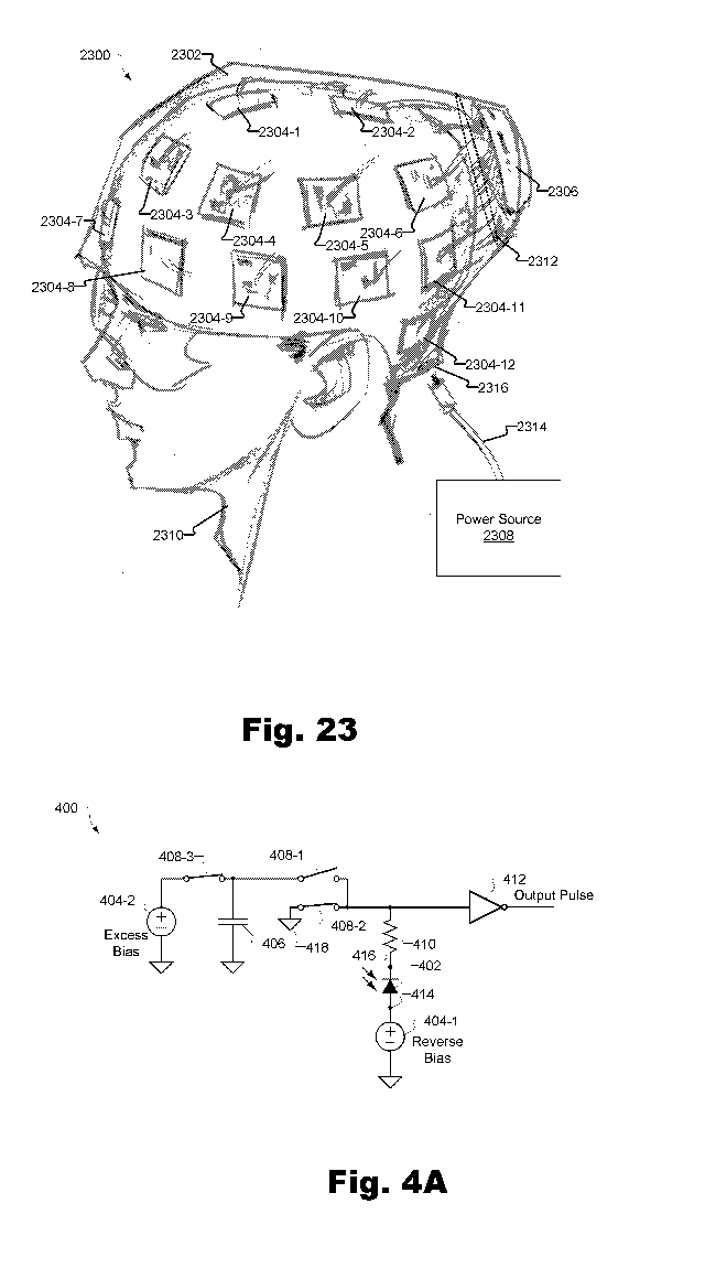
armed
state by connecting voltage source 1104-2 to input node 1116 of SPAD 1102
while
18
CA 03096824 2020-10-09
WO 2019/221784
PCT/US2018/062777
capacitor 1106-1 is both charged with the bias voltage and disconnected from
voltage
source 1104-1.
[0096] When voltage source 1104-2 is connected to input node 1116,
voltage source
1104-2 supplies the reverse excess bias voltage to input node 1116. This
causes the
.. voltage across SPAD 1102 to be greater than the breakdown voltage of SPAD
1102,
thereby putting SPAD 1102 in the armed state. For example, if the breakdown
voltage
of SPAD 1102 is 20 volts, the bias voltage as supplied by capacitor 1106-1 at
output
node 1114 is 18 volts when capacitor 1106-1 is fully charged, and the reverse
excess
bias voltage supplied by voltage source 1104-2 at input node 1116 is -3 volts,
the
voltage across SPAD 1102 is 21 volts, which is greater than the breakdown
voltage of
SPAD 1102.
[0097] Switch 1108-1 may put SPAD 1102 into a disarmed state by
disconnecting
voltage source 1104-2 from input node 1116 of SPAD 1102 and connecting input
node
116 of SPAD 1102 to ground 1118. In this configuration, the voltage across
SPAD 1102
is substantially equal to the magnitude of the bias voltage, which is less
than the
breakdown voltage of SPAD 1102.
[0098] Inverter 1112 is similar to inverter 412 and is configured to
generate an
output pulse when a photon hits SPAD 1102 while SPAD 1102 is in the armed
state.
When a photon initiates an avalanche within SPAD 1102, SPAD 1102 draws current
.. from capacitor 1106-1, which discharges capacitor 1106-1 to zero. As
capacitor 1106-1
is discharged, the voltage at output node 1114 decreases. When the voltage at
output
node 1114 drops below a certain value, inverter 1112 generates an output
pulse.
[0099] FIG. 11B shows an alterative implementation of SPAD circuit 1100
in which a
comparator 1120 is included in SPAD circuit 400 in place of inverter 1112.
Comparator
1120 is similar to comparator 420 and is configured to generate an output
pulse when a
photon hits SPAD 1102 while SPAD 1102 is in the armed state. As shown, a
positive
terminal of comparator 1120 is connected to output node 1114 of SPAD 1102 by
way of
capacitor 1106-2. In some examples, capacitor 1106-2 is omitted from SPAD
circuit
1100.
[0100] When a photon initiates an avalanche within SPAD 1102, SPAD 1102
draws
current from capacitor 1106-1, which discharges capacitor 1106-1 to zero. As
capacitor
1106-1 is discharged, the voltage at output node 1114 decreases. When the
voltage at
output node 1114 drops below the threshold voltage on the negative terminal of
comparator 1120, comparator 1120 generates an output pulse.
19
CA 03096824 2020-10-09
WO 2019/221784
PCT/US2018/062777
[0101] FIG. 12 is a flowchart 1200 that illustrates an exemplary mode of
operation of
SPAD circuit 1100. For purposes of this example, control circuit 206 is
configured to
control SPAD circuit 1100 by controlling switches 1108, TDC 208 is connected
to the
output of inverter 1112, and signal processing circuit 210 is connected to the
output of
TDC 208. One or more of the operations shown in flowchart 1200 may be
performed by
control circuit 206.
[0102] In operation 1202, capacitor 1106-1 is charged with the bias
voltage while
SPAD 1102 is in a disarmed state. Control circuit 206 may cause capacitor 1106-
1 to
be charged with the bias voltage while SPAD 1102 is in the disarmed state by
providing
.. control logic that causes switch 1108-1 to be in a first position (i.e.,
closed) to connect
input node 1116 of SPAD 1102 to ground 1118 and switch 1108-2 to be in the
first
position to connect voltage source 1104-1 to capacitor 1106-1. This switch
state is
shown in FIG. 11A.
[0103] While in the switch state shown in FIG. 11A, voltage source 1104-
1 charges
capacitor 1106-1 with the bias voltage. When control circuit 206 detects that
capacitor
1106-1 is fully charged with the bias voltage (Yes; decision block 1204),
control circuit
1206 disconnects voltage source 1104-1 from capacitor 1106-1 (operation 1206).
This
is performed by control circuit 1206 providing control logic that causes
switch 1108-2 to
be in the second position (i.e., open) while switch 1108-1 is still in the
first position. This
switch state is shown in FIG. 13.
[0104] In operation 1208, control circuit 206 puts SPAD 1102 in an armed
state
while capacitor 1106-1 is charged with the bias voltage. To this end, control
circuit 206
provides control logic that causes switch 1108-1 to be in the second position
(i.e., open)
to connect input node 1116 of SPAD 1102 to voltage source 1104-2. The control
logic
also keeps switch 1108-2 in the second position to keep voltage source 1104-1
disconnected from capacitor 1106-1. This switch state is shown in FIG. 14.
While in the
switch state shown in FIG. 14, SPAD 1102 is armed because the voltage across
SPAD
1102 is higher than the breakdown voltage of SPAD 1102.
[0105] As described above, control circuit 206 may arm and disarm SPAD
1102 in
accordance with a programmable gate delay and a programmable gate width.
Accordingly, if control circuit 206 detects that the programmable gate width
is met (i.e.,
that the predetermined time specified by the programmable gate width has
expired)
(Yes; decision block 1210), control circuit 206 puts SPAD 402 back in the
disarmed
state (operation 1212) by causing switch 1208-1 to be in the first position to
connect
CA 03096824 2020-10-09
WO 2019/221784
PCT/US2018/062777
input node 1116 of SPAD 1102 to ground 1118. The process shown in FIG. 12 may
be
repeated for subsequent light pulses.
[0106] Once SPAD 1102 has been put in the armed state, a photon from the
light
pulse may initiate an avalanche within SPAD 1102. As described above, SPAD
1102
draws current from capacitor 1106-1 while the avalanche is occurring, which
decreases
the voltage at output node 1116. When the voltage at output node 1116 drops
below a
certain value, inverter 1112 generates an output pulse. TDC 208 may process
the
output pulse as described above.
[0107] The various components included in SPAD circuit 1100 may be
implemented
in any suitable manner. For example, switches 1108 may each be implemented by
any
suitable switch circuitry, such as the switch circuitry shown in FIGS. 9A-9F.
Inverter
1112 may be implemented by the circuitry shown in FIG. 10A. Comparator 1120
may
be implemented by the circuitry shown in FIG. 10B.
[0108] In some examples, inverter 1112 and comparator 1120 may be
omitted from
SPAD circuit 1100. In these examples, the output from SPAD 1102 is provided as
the
input to TDC 208.
[0109] SPAD circuit 1110 may be implemented by any of a number of
alternative
circuit topologies. For example, FIGS. 15-20 show alternative circuit
topologies of
SPAD circuit 1110. In particular, the circuit topology of FIG. 17 does not
include a
capacitor that gates the SPAD. Rather, the parasitic capacitance of the SPAD
is
charged with an excess bias voltage and used to gate the SPAD. This may
advantageous in configurations where space limitations limit the number of
components
that can be included in SPAD circuit 1110.
[0110] FIG. 21 illustrates an exemplary method 2100. While FIG. 21
illustrates
exemplary operations according to one embodiment, other embodiments may omit,
add
to, reorder, and/or modify any of the operations shown in FIG. 21. One or more
of the
operations shown in FIG. 21 may be performed by control circuit 206 in
connection with
SPAD circuit 400.
[0111] In operation 2102, control circuit 206 directs a first voltage
source to supply a
reverse bias voltage at an input node of a SPAD, the reverse bias voltage
having a
magnitude that is equal to or less than a breakdown voltage of the SPAD.
Operation
2102 may be performed in any of the ways described herein.
21
CA 03096824 2020-10-09
WO 2019/221784
PCT/US2018/062777
[0112] In operation 2104, control circuit 206 directs a second voltage
source
configured to selectively connect to a capacitor to charge the capacitor with
an excess
bias voltage. Operation 2104 may be performed in any of the ways described
herein.
[0113] In operation 2106, control circuit 206 disconnects, in response
to the
capacitor being charged with the excess bias voltage, the second voltage
source from
the capacitor. Operation 2106 may be performed in any of the ways described
herein.
[0114] In operation 2108, control circuit 206 puts the SPAD into an
armed state by
connecting the capacitor to an output node of the SPAD while the capacitor is
both
charged with the excess bias voltage and disconnected from the second voltage
source. Operation 2108 may be performed in any of the ways described herein.
[0115] FIG. 22 illustrates another exemplary method 2200. While FIG. 22
illustrates
exemplary operations according to one embodiment, other embodiments may omit,
add
to, reorder, and/or modify any of the operations shown in FIG. 22. One or more
of the
operations shown in FIG. 22 may be performed by control circuit 206 in
connection with
.. SPAD circuit 1100.
[0116] In operation 2202, control circuit 206 directs a first voltage
source to charge a
capacitor connected to an output node of a single photon avalanche diode with
a bias
voltage having a magnitude that is equal to or less than a breakdown voltage
of the
SPAD. Operation 2202 may be performed in any of the ways described herein.
[0117] In operation 2204, control circuit 206 directs a second voltage
source to
supply a reverse excess bias voltage. Operation 2204 may be performed in any
of the
ways described herein.
[0118] In operation 2206, control circuit 206 puts the SPAD into an
armed state by
connecting the second voltage source to an input node of the SPAD while the
capacitor
is both charged with the bias voltage and disconnected from the first voltage
source.
Operation 2206 may be performed in any of the ways described herein.
[0119] Various non-invasive wearable brain interface systems that may
implement
the photodetector architectures described herein will now be described in
connection
with FIGS. 23-29. Each of the non-invasive wearable brain interface systems
described
in connection with FIGS. 23-29 will be referred to as "brain interface
systems". The
brain interface systems described herein are merely exemplary of the many
different
types of brain interface systems that may implement the photodetector
architectures
described herein.
22
CA 03096824 2020-10-09
WO 2019/221784
PCT/US2018/062777
[0120] FIG. 23 shows an exemplary brain interface system 2300. Brain
interface
system 2300 includes headgear 2302, a plurality of photodetector units 2304
(e.g.,
photodetector units 2304-1 through 2304-12), a master control unit 2306, and a
power
source 2308.
[0121] In the example of FIG. 23, headgear 2302 is implemented by a cap
that is
worn on a head of a user 2310. Alternative implementations of headgear 2302
include
helmets, beanies, headbands, other hat shapes, etc. and will be described
herein.
Headgear 2302 may be made out of any suitable cloth, soft polymer, plastic,
hard shell,
and/or any other suitable material as may serve a particular implementation.
[0122] Photodetector units 2304 may be attached to headgear 2302 in any
suitable
manner. For example, headgear 2302 may include a plurality of cutouts within
which
photodetector units 2304 are configured to fit, a plurality of protrusions on
an inner
surface of headgear 2302 to which photodetector units 2304 are configured to
attached,
a plurality of embedded housings configured to enclose individual
photodetector units
2304, and/or any other suitable attachment mechanism or element.
[0123] To illustrate, FIG. 24A shows an exemplary portion of headgear
2302 that
includes a plurality of cutouts 2402 (e.g., cutout 2402-1 through cutout 2402-
9). In FIG.
24A, photodetector units 2304 have not yet been inserted within cutouts 2402.
As
shown, each cutout 2402 may be surrounded by a rigid ring 2404 embedded within
.. headgear 2302. For example, cutout 2402 is surrounded by rigid ring 2404.
Rigid rings
2404 may be made out of any suitable material (e.g., plastic, metal, etc.).
Rigid rings
2404 may include one or more grooves or other features configured to
facilitate
removable attachment of photodetector units 2304 to headgear 2302. While
cutouts
2402 and rigid rings 2404 are shown in FIG. 24A to be rectangular, cutouts
2402 and
.. rigid rings 2404 may alternatively be any other shape and/or size.
[0124] FIG. 24B shows a cross sectional side view of headgear 2302 and
illustrates
an alternative configuration in which headgear 2302 includes a plurality of
protrusions
2406 (e.g., protrusions 2406-1 through 2406-5). Protrusions 2406 may be made
out of
the same or a different material as headgear 2302 and may be located on an
inner
surface of headgear 2302. While shown in FIG. 24B to be separate elements that
are
coupled to headgear 2302, protrusions 2406 may alternatively be formed as part
of
headgear 2302. Protrusions 2406 may have any suitable shape and/or size that
allows
photodetector units 2304 to attach thereto. In some examples, protrusions 2406
each
23
CA 03096824 2020-10-09
WO 2019/221784
PCT/US2018/062777
include a rigid ring similar to rigid rings 2404 to which photodetector units
2304 may
attach.
[0125] In some alternative examples, photodetector units 2304 are not
attached to
headgear 2302 in discrete locations. For example, headgear 2302 may include a
rail-
like guide inside headgear 2302 that allows a user to position photodetector
units 2304
anywhere along a continuous path instead of in discrete cutout or protrusion
locations.
As another example, headgear 2302 may be made out of a magnetic material to
which
photodetector units may magnetically couple at any desirable location.
[0126] The above-described manners in which photodetector units 2304 may
attach
to headgear 2302 may similarly apply to any of the other brain interface
systems
described herein.
[0127] Returning to FIG. 23, each photodetector unit 2304 may be self-
contained. In
other words, each photodetector unit may be housed within its own casing. Each
photodetector unit 2304 may be similar to photodetector system 300. For
example,
each photodetector unit 2304 may include an individual light source configured
to
generate light and a plurality of photodetectors configured to detect photons
of the light
after the photons reflect from a target within a brain of user 2310. In some
examples,
each photodetector unit 2304 may include a printed circuit board on which the
light
source and the photodetectors are disposed.
[0128] In some alternative embodiments, photodetector units 2304 do not
include
individual light sources. Instead, a light source configured to generate the
light that is
detected by photodetector units 2304 may be included elsewhere in brain
interface
system 2300. For example, a light source may be included in master control
unit 2306
and coupled to photodetector units 2304 through electrical connections.
[0129] Each of the light sources described herein may be implemented by any
suitable device. For example, a light source as used herein may be, for
example, a
distributed feedback (DFB) laser, a super luminescent diode (SLD), a light
emitting
diode (LED), a diode-pumped solid-state (DPSS) laser, a laser diode (LD), a
super
luminescent light emitting diode (sLED), a vertical-cavity surface-emitting
laser
(VCSEL), a titanium sapphire laser, a micro light emitting diode (mLED),
and/or any
other suitable laser or light source.
[0130] Each photodetector included in the plurality of photodetectors
may be
implemented by any of the photodetectors described herein. For example, a
particular
photodetector included in the plurality of photodetectors may include a SPAD
and a
24
CA 03096824 2020-10-09
WO 2019/221784
PCT/US2018/062777
capacitor. The capacitor is configured to be charged, while the SPAD is in a
disarmed
state, with a bias voltage by a voltage source. The capacitor is configured to
supply,
when the SPAD is put in an armed state, the bias voltage to an output node of
the
SPAD such that a voltage across the SPAD is greater than a breakdown voltage
of the
SPAD.
[0131] Master control unit 2306 is communicatively coupled to each of
photodetector
units 2304 by way of a plurality of wires 2312. In some examples, wires 2312
are at
least partially tunneled from photodetector units 2304 to master control unit
2306 within
a material of headgear 2302. In some examples, each photodetector unit 2304
includes
a plug interface configured to connect to one or more of wires 2312.
[0132] Master control unit 2306 may be configured to control
photodetector units
2304. For example, master control unit 2306 may direct the light source of
each
photodetector unit 2304 to generate the light in the photodetectors of each
photodetector unit 2304 to detect the photons of the light. This may be
performed in any
of the ways described herein.
[0133] As shown, master control unit 2306 is located within headgear
2302. In
alternative embodiments, as will be described below, master control unit 2306
may be
configured to be worn off the head of user 2310. In some examples, master
control unit
2306 may be selectively removed from headgear 2302.
[0134] Power source 2308 may be implemented by a battery and/or any other
type
of power source configured to provide operating power to master control unit
2306,
photodetector units 2304, and/or any other electronic component included
within brain
interface system 2300. As shown, power source 2308 may be connected to a power
cable 2314 that is configured to plug into a corresponding input power port
2316 of
master control unit 2306. In the example of FIG. 23, input power port 2316 is
connected
to master control unit 2306 by way of a wire (not shown). In alternative
examples, input
power port 2316 may be integrated directly into master control unit 2306. In
the
example of FIG. 23, power source 2308 is configured to be worn off the head of
user
2310. Alternatively, power source 2308 may be integrated into headpiece 2302.
For
example, power source 2308 may be configured to be worn on the shoulders
and/or
waist of user 2310, clip onto a belt worn by user 2310, and/or otherwise be
carried by
user 2310.
[0135] FIG. 25 shows another exemplary brain interface system 2500. Like
brain
interface system 2300, brain interface system 2500 includes headgear 2502 and
a
CA 03096824 2020-10-09
WO 2019/221784
PCT/US2018/062777
plurality of photodetector units 2504 (e.g., photodetector units 2504-1
through 2504-4)
selectively attached to headgear 2502. However, in brain interface system
2500, the
master control unit and power source are both included in a self-contained
unit 2506
configured to be worn on the shoulders of a user 2508. The master control unit
and
power source included in unit 2506 are configured to perform the same
functions as
described in connection with FIG. 23. However, because the master control unit
and
power source are included in unit 2506, they are not explicitly illustrated in
FIG. 25.
[0136] FIG. 26 shows another exemplary brain interface system 2600.
Brain
interface system 2600 is similar to brain interface system 2300 in that brain
interface
system 2600 includes headgear 2602, plurality of photodetector units (e.g.,
photodetector unit 2604) selectively attached to headgear 2602, and a master
control
unit 2606 included in headgear 2602. However, in FIG. 26, headgear 2602 is
implemented by a beanie configured to be worn by a user 2608.
[0137] FIG. 27 shows another exemplary brain interface system 2700. In
brain
interface system 2700, headgear 2702 is implemented by a headband configured
to be
worn by a user 2704. Like brain interface system 2300, brain interface system
2700
includes headgear 2702 and a plurality of photodetector units 2704 selectively
attached
to headgear 2702. A plurality of photodetector units (e.g., photodetector unit
2706) are
selectively attached to headgear 2702, as described above. In brain interface
system
2700, the master control unit and power source are included in a self-
contained unit
2708 configured to be worn on the shoulders of user 2704.
[0138] FIG. 28 shows an inner surface of headgear 2802 that may be
included in
any of the brain interface systems described herein. Headgear 2802 may be
configured
to hug (e.g., conform to) the head of a user. The inner surface is configured
to face the
head of a user while the user wears headgear 2802. As shown, a plurality of
photodetector units (e.g., photodetector unit 2804) may be attached to
headpiece 2802
(e.g., by fitting within a plurality of cutouts of headpiece 2802, attaching
to a plurality of
protrusions of headpiece 2802, being enclosed within a plurality of embedded
housings
of headpiece 2802, etc.). As described above, each photodetector unit includes
a light
source configured to direct light into the brain of the user. For example,
photodetector
unit 2804 includes light source 2806. Light source 2806 can be part of or
included
within the photodetector unit 2804, as shown, or alternatively light source
2806 may be
remotely located and coupled to photodetector unit 2804 through electrical
connections.
26
CA 03096824 2020-10-09
WO 2019/221784
PCT/US2018/062777
[0139] FIG. 29 shows another exemplary brain interface system 2900.
Brain
interface system 2900 includes headgear 2902 configured to be worn by a user
2904
and includes a master control unit 2906 and a plurality of photodetector units
(not
shown). Master control unit 2906 is connected to a power source 2908 by way of
a
.. power cable 2910. Headgear 2902 is similar to headgear 2802 in that
headgear 2902 is
configured to hug the head of user 2904.
[0140] As shown, power source 2908 may be attached to a belt 2912 that may be
worn by user 2904. In this configuration, power source 2908 remain securely
attached
to user 2904 while the user 2904 runs or otherwise moves.
[0141] In the preceding description, various exemplary embodiments have
been
described with reference to the accompanying drawings. It will, however, be
evident
that various modifications and changes may be made thereto, and additional
embodiments may be implemented, without departing from the scope of the
invention
as set forth in the claims that follow. For example, certain features of one
embodiment
.. described herein may be combined with or substituted for features of
another
embodiment described herein. The description and drawings are accordingly to
be
regarded in an illustrative rather than a restrictive sense.
27