Note: Descriptions are shown in the official language in which they were submitted.
CA 03098883 2020-10-29
WO 2019/222648
PCT/US2019/032900
TITLE OF THE INVENTION
[0001] Headset Communication System
CROSS-REFERENCE TO RELATED APPLICATIONS
[0002] This application claims the benefit of U.S. Provisional Patent
Application No.
62/673,836 filed May 18, 2018 entitled "Headset Communication System" and U.S.
Provisional
Patent Application No. 62/673,599 filed May 18, 2018 entitled "Communication
Handset", both of
which are incorporated by reference herein in their entireties.
FIELD OF THE INVENTION
[0003] The present invention generally relates to a headset
communication system and, more
particularly, to systems, methods and apparatuses for improved headset
communications with
external sources.
BRIEF DESCRIPTION OF THE SEVERAL VIEWS OF THE DRAWINGS
[0004] The following detailed description of embodiments of the
communication headset will be
better understood when read in conjunction with the appended drawings of an
exemplary
embodiment. It should be understood, however, that the invention is not
limited to the precise
arrangements and instrumentalities shown.
[0005] In the drawings:
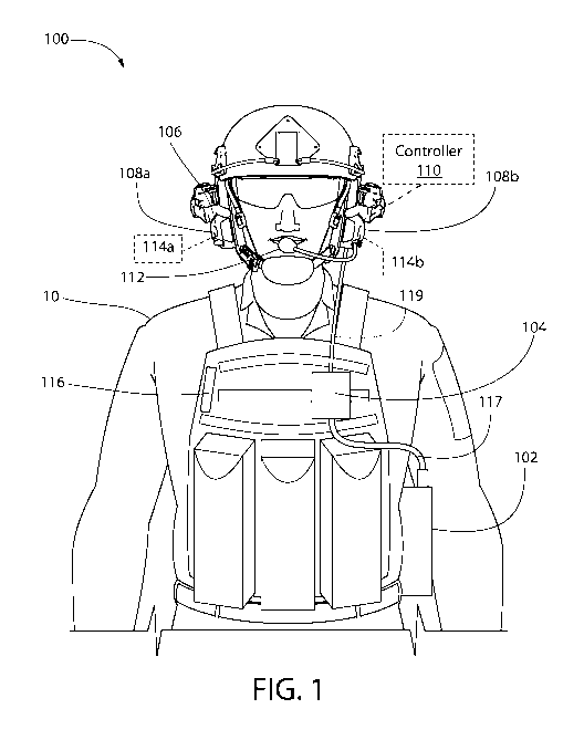
[0006] Figure 1 is a schematic representation of an exemplary
communication system for a user,
according to at least one embodiment of the invention;
[0007] Figure 2 is a schematic representation of a portion of the
communication system of
Figure 1 for limiting peak values of an audio signal produced for the user,
according to at least one
embodiment of the invention;
[0008] Figure 3A is a conceptual representation of a portion of the
communication system of
Figure 1 for a low distortion transmission of an audio signal produced for the
user, according to at
least one embodiment of the invention;
[0009] Figure 3B is a schematic representation of the failsafe bypass
module of Figure 3A,
according to at least one embodiment of the invention;
[0010] Figure 4 is a schematic representation of an exemplary receive
module implementable in
the push-to-talk handset of Figure 1, according to at least one embodiment of
the invention;
1
CA 03098883 2020-10-29
WO 2019/222648
PCT/US2019/032900
[0011] Figures 5A-5E are top perspective, front, top, bottom, and bottom
perspective views,
respectively, of the handset of Figure 1, according to at least one embodiment
of the invention;
[0012] Figure 6 is a conceptual representation of the controller
wirelessly communicating with
an external manufacturing controller, according to at least one embodiment of
the invention;
[0013] Figure 7 is a schematic representation of the transmit module of
Figure 6 according to at
least one embodiment of the invention;
[0014] Figures 8A-8B are a schematic representation of the receive
module of Figure 6
according to at least one embodiment of the invention; and
[0015] Figure 9 includes multiple plots representing the electrical
signal at a respective output
terminal of certain components in the transmit module of Figure 7 and the
receive module of Figures
8A-8B, according to at least one embodiment of the invention.
DETAILED DESCRIPTION OF THE EXEMPLARY EMBODIMENTS OF THE INVENTION
[0016] Referring to the drawings in detail, wherein like reference
numerals indicate like
elements throughout, there is shown in Figs. 1-9 a communication system 100
for a user 10,
generally designated, in accordance with an exemplary embodiment of the
present invention.
[0017] Referring to Figure 1, the communication system 100 may include
at least one of: a radio
102, a push-to-talk (PTT) handset 104, a headset 106 which may include right
and left earcups 108a-
108b, a controller 110, a microphone 112, and right and left ambient sound
microphones 114a-114b.
[0018] The radio 102 may be configured to transmit and/or receive radio
signals using an
antenna. In some embodiments, the radio 102 may be a plurality of radios, each
configured to
receive a separate and distinct radio signal. The radio 102 may be configured
to decode or
demodulate the radio signals and provide an audio signal representative of the
radio signals that can
be used by the headset 106 and earcups 108a-b to drive a speaker configured to
produce sounds
audible to the user 10. In addition, the radio 102 may be configured to
receive audio signals from
the microphone 112, encode or modulate the audio signals, and transmit radio
signals representative
of the audio signal to external sources (e.g., another radio).
[0019] The handset 104 may be configured to toggle the radio 102 between
transmission and
reception of the radio signals. Handset 104 may be connected to radio 102
through cable 117 and
may be connected to headset 106 via cable 119. The radio 102 may be toggled by
the user via the
handset 104. For example, the handset 104 may include a pushbutton (not
shown). If the
pushbutton is activated by the user, the handset 104 toggles the radio 102 to
operate in a
transmission mode. In the transmission mode, the handset 104 may toggle the
radio 102 to transmit
2
CA 03098883 2020-10-29
WO 2019/222648
PCT/US2019/032900
an audio signal received from the microphone 112. If the pushbutton is not
activated by the user, the
handset 104 toggles the radio 102 to operate in a reception mode. In the
reception mode, the handset
104 may receive an audio signal from an external source terminal and deliver
it to the left and right
earcups 108a-108b.
[0020] The handset 104 may be configured to transmit and receive audio
signals over multiple
radio channels. As used herein, the term "channel" may refer to a band of
frequencies that
correspond to a radio signal. The handset 104 may include a plurality of radio
channel ports, each
configured to receive a radio channel from one or more radios. One or more
pushbuttons may be
assigned to one or more radio channel ports to toggle the radios between
transmission and reception
of radio signals.
[0021] The handset 104 may be couplable to an accessory or clothing. In
one embodiment, the
handset 104 is removably coupled to a strap extending across a user's chest
such that the handset is
quickly accessible by at least one hand. In one embodiment, the handset is
configured to couple to
webbing 116. Webbing 116 may be modular lightweight load-carrying equipment
(e.g., MOLLE)
webbing or pouch attachment ladder system (PALS) webbing, among others. In
some
embodiments, the webbing 116 is comprised of heavy-duty nylon. The webbing 116
may be
stitched onto a vest of the user 10 to allow for the attachment of various
compatible pouches and
accessories. The webbing 116 may include one or more horizontal rows of
approximately 1 inch
(2.5 cm) webbing. Each of the horizontal rows of the webbing 116 may be spaced
1 inch apart. The
webbing 116 may be attached to a backing at 1.5 inch (3.8 cm) intervals.
[0022] Microphone 112 may be configured to convert sound produced by the
user into an
electrical audio signal. The electrical audio signal from the microphone 112
may be transmitted to
the radio 102 for wireless broadcasting.
[0023] The controller 110 may be configured to improve communication
functionality for this
user. In some embodiments, the controller 110 is a microprocessor having
memory. The memory
may include one or more programs that when executed by a processor, cause the
processor to
perform one or more functions described herein. In some embodiments, the
controller may include
passive electrical components that are configured to process audio signals to
perform one or more
functions described herein.
[0024] Hear-Through Limiter
[0025] With continued reference to Figure 1, right and left ambient
sound microphones 114a-b
may be configured to convert external sound around the user into an electrical
audio signal. The
electrical audio signal from the right and left ambient sound microphones 114a-
b may be transmitted
3
CA 03098883 2020-10-29
WO 2019/222648
PCT/US2019/032900
to the earcups 108a-b to drive a speaker configured to produce sounds audible
to the user 10.
Depending on the application or circumstance, the earcups 108a-108b can be
configured to muffle
external ambient sounds for the user to allow the user to hear a radio
communication more clearly.
However, in other instances the user may need to hear external ambient sounds
to properly observe
the user's surroundings. In certain instances, such as when there is no
received radio
communication, the ambient sound microphones 114a-114b are configured to allow
the user to hear
external ambient sounds even if the earcups 108a-108b have a sound muffling
effect on the user's
hearing ability.
[0026] Figure 2 is a representation of a portion of the communication
system 100 of Figure 1 for
.. limiting peak values of an audio signal produced for the user 10, according
to at least one
embodiment of the invention. As discussed above, and also as illustrated in
Figure 2, the
communication system 100 may include right and left ambient sound microphone
114a-b to allow a
user 10 to hear surroundings while wearing headset 106 and potentially sound-
muffling earcups
108a-108b. The audio signals from the right and left ambient sound microphone
114a-b are
.. processed by controller 110 before being transmitted to the right and left
ear speakers 207a-b,
positioned within the earcups 108a-b for producing sound audible to the user
10. In some
embodiments, the controller 110 includes a hear-through limiter module 201
configured to prevent
unsafe sound levels from reaching the ear of the user 10 by actively adjusting
and attenuating the
hear-through gain to keep the sound level below a set limit. The audio signal
received at the hear-
through limiter module 201 may be monitored to estimate the instantaneous
level of that signal and
the gain may be dynamically adjusted to control the sound reaching the ear of
the user. To adjust
the gain appropriately, the two signals may be compared and the signal with
the highest
instantaneous level may be used to determine the gain needed to control the
sound reaching both
ears.
[0027] The hear-through limiter module 201 may include at least one of a
sidechain filter
module 213, right ear peak envelope module 209a, left ear peak envelope module
209b, compare
module 211, limiter module 203 and equalizer module 205.
[0028] The sidechain filter module 213 may receive the right ear audio
signal from right ambient
sound microphone 114a and the left ear audio signal from left ambient sound
microphone 114b. In
.. some embodiments, the right ear audio signal and left ear audio signal may
be replaced by another
audio signal representative of sound. In some embodiments, the right and left
ambient sound
microphones 114a-b are replaced by another audio source configured to produce
an audio signal.
The sidechain filter module 213 may be configured to limit modulation applied
to the left ear audio
4
CA 03098883 2020-10-29
WO 2019/222648
PCT/US2019/032900
signal and the right ear audio signal at certain frequencies. To adjust the
frequency-dependent
behavior of the hear-through limiter module 201 without affecting the
frequency content of the
sound reaching the ear, the hear-through signals may be cloned and then passed
to the sidechain
filter module 213 prior to being used to determine the signal gain at the
limiter module 203. Using
the sidechain filter module 213, specific frequency ranges can be emphasized
or deemphasized. For
example, at certain frequencies, the decibels may be limited to approximately
95dB, 85dB, or 75dB.
[0029] In some embodiments, the right ear (RE) peak envelope module 209a
and the left ear
(LE) peak envelope module 209b may each receive the corresponding right or
left filtered audio
signal from sidechain filter 213. Alternatively, in some embodiments that do
not include the
sidechain filter 213, right ear peak envelope module 209a and the left ear
peak envelope module
209b may each receive the right ear audio signal from right ambient sound
microphone 114a and the
left ear audio signal from left ambient sound microphone 114b. The peak
envelope modules 209a-b
each may calculate an instantaneous peak value representative of the magnitude
of the received
filtered audio signal at predetermined sampling intervals. In some
embodiments, the sampling
interval is approximately 32 kHz. In one embodiment, the sampling interval of
approximately 32
kHz is used for one or more modules shown in Fig. 2. The peak envelope modules
209a-b each may
compute the instantaneous value of the magnitude of the received filtered
audio signal using an
exponential decaying peak hold function. The peak envelope modules 209a-b each
may compare a
current peak value of a sampled audio signal to a previous peak value of the
sampled audio signal.
The peak envelope modules 209a-b each may determine whether the current peak
value of the
sampled audio signal is greater than, or less than, the previous peak value of
the sampled audio
signal. In response to a determination that the current peak value of the
sampled audio signal is
greater than the previous peak value of the sampled audio signal, the
respective peak envelope
module 209a-b may output the current peak value of the sampled audio signal.
In response to a
determination that the current peak value of the sampled audio signal is less
than the previous peak
value of the sampled audio signal, the respective peak envelope module 209a-b
may output the
previous peak value of the sampled audio signal.
[0030] In one embodiment, by using an exponentially decaying peak hold
function, the peak
envelope modules 209a-b minimizes the number of times that switching occurs
between the two
different audio signals in later steps. In some embodiments, the exponentially
decaying function (A)
is:
A = Ao * e_(t-)
wherein:
5
CA 03098883 2020-10-29
WO 2019/222648
PCT/US2019/032900
Ao is a measured peak value of an audio signal,
k is a rate of decay,
h is a hold time before the exponential decaying function is initiated,
t is time.
In some embodiments, the hold time (h) is 0 ms. In some embodiments, the rate
of decay (k) is
1000 s-1.
In some embodiments, the output of the peak envelope module (y) is:
if A> c * y(ti)
Y(t2) = r A
tc * y(q) if A c * y(q)
Wherein:
A is a measured peak value of an audio signal,
c is a decay coefficient, with a value between 0 and 1,
y(ti) is the previous value of the peak envelope module 204 output,
y(t2) is the new value of the peak envelope module 204 output.
[0031] While Figure 2 shows right ear peak envelope module 209a and left
ear peak envelope
module 209b, in some embodiments, a single peak envelope module may be used to
perform any of
the functionality described with respect to the right ear peak envelope module
209a and left ear peak
envelope module 209b.
[0032] Compare module 211 may receive a right ear instantaneous peak
value from the right ear
peak envelope module 209a and a left ear instantaneous peak value from the
left ear peak envelope
module 209b. Compare module 211 may receive a right ear audio signal and a
left ear audio signal
from sidechain filter 213. Alternatively, in some embodiments that do not
include the sidechain filter
213, compare module 211 may receive a right ear audio signal and a left ear
audio signal from the
right ambient sound microphone 114a and the left ambient sound microphone
114b. The compare
module 211 may generate a peak comparison audio signal representative of
either the right ear audio
signal or the left ear audio signal based on whether the right ear
instantaneous peak value is greater
than, or less than, the left ear instantaneous peak value. For example, in
some embodiments,
compare module 211 may compare the right ear instantaneous peak value and the
left ear
instantaneous peak value. The compare module 211 may determine whether the
right ear
instantaneous peak value is greater than, or less than, the left ear
instantaneous peak value. In
response to a determination that the right ear instantaneous peak value is
greater than the left ear
instantaneous peak value, the compare module 211 may generate or output a peak
comparison audio
6
CA 03098883 2020-10-29
WO 2019/222648
PCT/US2019/032900
signal representative of the right ear audio signal. In response to a
determination that the right ear
instantaneous peak value is less than the left ear instantaneous peak value,
the compare module 211
may generate or output a peak comparison audio signal representative of the
left ear audio signal.
[0033] Limiter module 203 may receive the left ear audio signal from the
left ear microphone
114b signal and the right ear audio signal from the right ear microphone 114a.
The limiter module
203 may also receive the peak comparison audio signal from the compare module
211. The limiter
module 203 may selectively attenuate the left ear microphone signal and the
right ear microphone
signal based on whether the peak comparison audio signal exceeds a
predetermined limit threshold.
For example, in some embodiments, the limiter module 203 may compare an
amplitude of the peak
comparison audio signal to the predetermined limit threshold and determine
whether the amplitude
of the peak comparison audio signal exceeds the predetermined limit threshold.
In response to a
determination that the amplitude of the peak comparison audio signal is
greater than the limit
threshold, the limiter module 203 may apply an attenuation factor to each of
the left ear audio signal
and the right ear audio signal. In some embodiments, the attenuation factor is
a ratio of the
predetermined limit threshold and the amplitude of the peak comparison audio
signal. In response to
a determination that the amplitude of the peak comparison audio signal is less
than the limit
threshold, the limiter module 203 may refrain from applying an attenuation
factor to each of the left
ear audio signal and the right ear audio signal.
[0034] In some embodiments, before the right ear audio signal and the
left ear audio signal are
transmitted to the right and left ear speakers 207a-b, the equalizer module
205 receives the left ear
audio signal and the right ear audio signal from the limiter module 203. The
equalizer module 205
may modify the left ear audio signal and the right ear audio signal using one
or more linear filters. In
some embodiments, the equalizer module 205 may modify the left ear audio
signal and the right ear
audio signal using one or more linear filters at certain frequencies.
Modifying the audio signals may
help offset the frequency response of the microphones 114a-b and the speakers
207a-b. Modifying
the audio signals may also help accentuate certain high or low frequencies.
The equalizer module
205 may then transmit the equalized right ear audio signal and the equalized
left ear audio signal to
the respective right and left ear speakers 207a-b for producing sound audible
to the user 10.
[0035] While the right and left ear speakers 207a-b are shown as
exemplary audio reception
devices in Figure 2, in some embodiment, other audio reception devices
configured to receive an
audio signal may be used.
[0036] In some embodiments, the positions of the limiter module 203 and
equalizer module 205
may be interchanged such that the limiter module 203, rather than the
equalizer module 205, may
7
CA 03098883 2020-10-29
WO 2019/222648
PCT/US2019/032900
transmit the equalized right ear audio signal and the equalized left ear audio
signal to the respective
right and left ear speakers 207a-b for producing sound audible to the user 10.
[0037] Low-Distortion Transmission Module
[0038] As discussed above, the communication system 100 may include an
audio source device
(e.g., radio 102 shown in Figure 1) that produces an audio signal transmitted
to speaker 207.
Referring to Figure 3A, the audio signal may be transmitted to speaker 207 via
controller 110. The
controller 110 may include a low distortion transmission module 300 configured
to drive the speaker
207. The low distortion transmission module 300 may include a power amplifier
302 and a failsafe
bypass module 304. If the controller 110 receives power from a power source,
such as a battery, the
power amplifier 302 is operable to amplify the audio signal to drive speakers
207 to produce audible
sound to the user 10. If the controller 110 does not receive power from the
power source, the power
amplifier 302 is inoperable to amplify the audio signal to drive speaker 207
to produce audible
sound to the user 10. Instead, the failsafe bypass module 304 may transfer the
audio signal to the
speaker 207, with the power from the audio signal driving the speaker 207 to
produce sound.
[0039] Referring to Figure 3B, the failsafe bypass module 304 may include
first and second
signal path transistors T1-T2 and a bypass activation transistor T3. The
bypass activation transistor
T3 and the first and second signal path transistors T1-T2 may operate in an
open state or a closed
state. When T3 is in an open state, the transistors T1-T2 operate similar to a
closed switch, where
current flows freely between the source terminal and drain terminal. In this
configuration, the
source terminal and drain terminal of the signal path transistors T1-T2 may
share a similar voltage
potential. When T3 is in a closed state, the transistors T1-T2 operate similar
to an open switch,
where current flow is impeded and the source terminal and drain terminal each
have independent
voltage potentials.
[0040] The first and second signal path transistors T1-T2 may be
junction gate field-effect
transistors. The bypass activation transistor T3 may be a bi-polar junction
transistor. In some
embodiments, transistors T1-T3 are replaced by other transistor types and
configurations that
perform similar functions to transistors T1-T3 as described herein.
[0041] The source terminal of the first and second signal path
transistors T1-T2 may be
connected (or also referred to herein as "in electrical communication with")
to the audio signal. In
one embodiment, the gate terminals of the first and second signal path
transistors T1-T2 are
connected to collector/drain of T3. The drain terminal of the first and second
signal path transistors
T1-T2 may be connected to the speaker 207. The drain terminal of the first and
second signal path
transistors T1-T2 may also be connected to the power signal, optionally via
resistor R1, to bias the
8
CA 03098883 2020-10-29
WO 2019/222648
PCT/US2019/032900
first and second signal path transistors T1-T2. The drain terminal of the
first and second signal path
transistors T1-T2 may be connected to the collector/drain terminal of the
bypass activation transistor
T3. In some embodiments, the drain terminal of the first and second signal
path transistors T1-T2
may be connected to the collector/drain terminal of the bypass activation
transistor T3 via a resistor
R2. The base/gate terminal of the bypass activation transistor T3 may be
connected to a control
signal provided from an external source terminal, such as a microprocessor.
The emitter/source
terminal of the bypass activation transistor T3 may be connected to ground.
[0042] In some embodiments, a capacitor Cl may be positioned between the
source terminal of
the first and second signal path transistors T1-T2 and the audio signal. In
some embodiments, a
.. capacitor C2 may be positioned between the drain terminal of first and
second signal path transistors
T1-T2 and the speaker 207. The capacitors C1-C2 may be approximately 100
microfarads. Using
capacitors C1-C2 may ensure that there is DC filtering of the audio signal
without interfering with
the audio band of the audio signal.
[0043] In some embodiments, a resistor R1 may be positioned between the
drain terminal of first
and second signal path transistors T1-T2 and the power signal. In some
embodiments, a resistor R2
may be positioned between the drain terminal of first and second signal path
transistors T1-T2 and
the collector/drain terminal of the bypass activation transistor T3. The
resistor R1 may be
approximately 10k Ohms. The resistor R2 may be approximately 500k Ohms. The
resistors R1-R2
may bias the first and second signal path transistors T1-T2 to operate in a
closed state while
receiving power via the power signal.
[0044] In some embodiments, a resistor R3 may be positioned between the
base/gate terminal of
the bypass activation transistor T3 and the control signal. The resistor R3
may be approximately
100k Ohms. The resistor R3 along with bypass activation transistor T3 may be
configured to
control the first and second signal path transistors T1-T2 via the control
signal without using a lot of
power from any external power source terminals for the failsafe bypass module
304.
[0045] If power is provided to the controller 110 in Figure 3A, the
power signal and/or control
signal of Figure 3B may be logic level high (also referred to herein as "a
high level"). In response to
the power signal and/or control signal being logic level high, the bypass
activation transistor T3 may
operate in a closed state. While the bypass activation transistor T3 operates
in a closed state, the
collector/drain terminal of the bypass activation transistor T3 may be pulled
to ground turning off
first and second signal path transistors T1-T2. In addition, the gate
terminals of the first and second
signal path transistors T1-T2 may also be connected to ground. In response to
the gate terminals of
the first and second signal path transistors T1-T2 being connected to ground,
the first and second
9
CA 03098883 2020-10-29
WO 2019/222648
PCT/US2019/032900
signal path transistors T1-T2 may operate in an open state. While the first
and second signal path
transistors T1-T2 operate in an open state, the audio signal may not pass
through to speaker 207.
Instead, as shown in Figure 3A, the audio signal will be transmitted to
speaker 207 via the amplifier
302.
[0046] If power is lost and not provided to the controller 110 in Figure
3A, the power signal and
control signal of Figure 3B may be logic level low (also referred to herein as
"a low level"). In
response to the power signal and control signal being logic level low, the
bypass activation transistor
T3 may operate in an open state. If the bypass activation transistor T3
operates in an open state, the
emitter/source terminal and collector/drain terminal of the bypass activation
transistor T3 may have
independent voltage potentials. If power is lost and not provided to the
controller 110 in Figure 3A,
the audio signal may leak through the source terminal of the first and second
signal path transistors
T1-T2 to the gate terminal of the first and second signal path transistors T1-
T2 via the drain terminal
of the first and second signal path transistors. The leaked audio signal may
cause the first and
second signal path transistors T1-T2 to automatically operate in a closed
state, a phenomenon also
known as "self turn on." The audio signal may pass to the speaker 207 to drive
the speaker 207 to
produce sound audible to the user 10.
[0047] "Self turn on" can result in an increase in total harmonic
distortion in the audio signal. If
the failsafe bypass module 304 is partially on while the main power amplifier
302 is on, the audio
signal sums into the audio path and causes signal distortion. As used herein,
the term total harmonic
distortion refers to the distortion produced by an amplifier (e.g., speaker
207), as measured in terms
of the harmonics of the sinusoidal components of the signal that the signal
introduces. As the total
voltage of the input audio signal increases, total harmonic distortion
increases without increasing
fundamental audio signal. In some embodiments, and as shown in Figure 3B, the
first and second
signal path transistors T1-T2 may be electrically connected in parallel. By
connecting the first and
second signal path transistors T1-T2 in parallel, impedance caused by the
first and second signal
path transistors T1-T2 is reduced. Reducing the impedance caused by the first
and second signal
path transistors T1-T2, reduces the effects of "self turn on" and total
harmonic distortion on the
audio signal decreases while maintaining the voltage of the audio signal
transmitted to the speaker
207 to drive the speaker 207 to produce sound audible to the user 10.
[0048] While a speaker 207 is shown in Figures 3A-3B, other audio reception
devices may be
used in some embodiments, including, but not limited to a transmission coil
that transmits an
electromagnetic signal using near-field magnetic induction to a corresponding
earplug that includes
CA 03098883 2020-10-29
WO 2019/222648
PCT/US2019/032900
a receiving coil configured to receive the electromagnetic signal, and a
speaker configured to
produce sound based on the electromagnetic signal.
[0049] Multichannel Mixing Passive PTT
[0050] Referring back to Figure 1, in some embodiments, the
communication system 100 may
include a push-to-talk handset 104. The push-to-talk handset 104 may be a
device that allows for
instantaneous communication with others. The push-to-talk handset 104 may
include user-
selectable button to switch the push-to-talk handset 104 from voice
transmission mode to voice
reception mode. In some embodiments, the push-to-talk handset 104 may include
multichannel
functionality, meaning the push-to-talk handset 104 can receive separate and
distinct audio signals
from one or more audio sources. For multichannel functionality, the electronic
circuitry can be
complex and may require external power, further programming and/or additional
training prior to
use. Thus, there is a need for a push-to-talk handset 104 that is usable
without programming or
significant adjustments ("plug and play"), easy to use, and does not require
an internal or alternate
power source.
[0051] Referring to Figure 4, the receive module 502 may be configured to
receive a plurality of
audio reception signals from one or more audio sources and produce a
corresponding audio
transmission signal representative of the sum of the audio reception signals.
For example, in Figure
4, the receive module may receive audio reception signals named first audio
reception signal and
second audio reception signal. The audio reception signals may be received
from any audio source,
such as radio 102 shown in Figure 4 or an intercom, among others.
[0052] The receive module 502 may include one or more summing resistors.
Each of the
summing resistors may receive a respective audio reception signal at a
respective first terminal of
each summing resistor. For example, as shown in Figure 4, the receive module
502 may include a
first summing resistor R51 and a second summing resistor R52. The first
summing resistor R51
may receive the first audio reception signal at a first terminal 506a of the
summing resistor R51.
The second summing resistor R52 may receive the second audio reception signal
at a first terminal
506b of the summing resistor R52.
[0053] Each of the summing resistors may include second terminals that
are each connected at a
summing node. For example, as shown in Figure 4, the first summing resistor
R51 and the second
summing resistor R52 include second terminals 508a-b, respectively, that are
each connected at a
summing node 510. At the summing node 510, due to the configuration of the
summing resistors,
the first audio reception signal and the second audio reception signal are
summed to create a
summed audio signal. By summing the audio reception signals using passive
components such as
11
CA 03098883 2020-10-29
WO 2019/222648
PCT/US2019/032900
resistors and transformers, the push-to-talk handset 104 can generate the
summed audio signal
without the use of external power sources, such as a battery or external DC
power.
[0054] The receive module 502 may include a transformer TR53. The
transformer TR53 may
be configured to receive the summed audio signal at summing node 510 and
produce an audio
transmission signal at node 514. The audio transmission signal may be
transmitted to an audio
reception device configured to receive an audio signal. For example, in Figure
4, the audio
reception device is headset 106.
[0055] The transformer TR53 may include a first coil 516a and a second
coil 516b. The first
coil 516a may include a first terminal 518a and a second terminal 518b. The
first terminal 518a may
be connected to summing node 510. The second terminal 518b may be connected to
an audio source
ground signal. By being connected to an audio source ground signal, the
transformer TR53 can
allow the push-to-talk handset 104 to "float the ground" or isolate the
grounds from input to output
so that the first and second audio reception signals may be received from two
separate audio sources
with their respective returns connected together. In Figure 4, transformer
TR53 may float the
ground represented by the audio source ground signal. The second coil 516b may
include a first
terminal 518c and a second terminal 518d. The second coil 516b may produce the
audio
transmission signal at first terminal 518c in response to receiving the summed
audio signal at
summing node 510. The second terminal 518d may be connected to ground.
[0056] In some embodiments, the components of the receive module 502 may
be duplicated to
add a separate and distinct second audio transmission signal summed from a
second set of audio
reception signals.
[0057] In some embodiments, additional audio reception signals can be
added to the receive
module 502 by also adding, for each additional audio reception signal, a
corresponding resistor that
connects to summing node 510.
[0058] In some embodiments, receive module 502 may be duplicated such that
two or more
separate and distinct receive modules are configured to receive one or more
audio transmission
signals and each produce separate and distinct combined audio transmission
signals that each may
be transmitted via a cable to an ear of the user.
[0059] Referring now to Figure 5A, the handset 104 may be generally
rectangular in shape. In
one embodiment, the corners of the handset 104 are rounded or angled. The
outer surface and edges
may be convex or shaped to provide a distinctive appearance and to provide
comfort in the palm of a
user's hand when the user grabs the handset to actuate one or more of the
buttons and discussed
below. In one embodiment, the back surface is substantially flat. The back
surface may be
12
CA 03098883 2020-10-29
WO 2019/222648
PCT/US2019/032900
substantially flat to allow for rotation of the handset relative to the
attachment clips as discussed in
further detail below. In other embodiments, the back surface is concave or
curved to conform to the
accessory or clothing that the handset 104 is attached to. The front surface
of the handset 104 may
include a decal pocket 202. The decal pocket 202 may include a recessed area
to help align a decal
applied to the handset 104 and help protect the peripheral edge of the decal
from peeling off of the
handset 104.
[0060] The handset 104 may include one or more channels. In some
embodiments, the handset
104 may include one, two, three or four channels. Each of the one or more
channels may be a
separate and distinct audio signal received from one or more radios, such as
radio 102 in Figure 1.
In some embodiments, the one or more radios may be dual-channel. As used
herein, the term "dual-
channel" may refer to a radio that provides two or more distinct audio
signals.
[0061] The handset 104 may include a plurality of buttons (e.g., buttons
204c-d in Figure 5A
and buttons 204a-b in Figure 5E) (also referred to herein as switches). In
Figure 5A, two buttons
204c-d are positioned on a first sidewall 206a of the handset 104. In Figure
5E, the two other
buttons 204a-b are positioned on a second sidewall 206b of the handset 104.
Each of the buttons
204a-d may be labeled with indicia (e.g., A, B, C, or D as shown in Figure 5A)
to identify the
respective button to the user 10. Each of the buttons 204a-d may correspond to
at least one separate
and distinct channel. Each button may operate in an on state and an off state.
When selected, the
corresponding button operates in an on state where the handset 104 receives a
user speech audio
signal representative of speech from a headset of a user and selectively
transmits the user speech
audio signal from a radio connected to a corresponding channel. The first
sidewall 206a and second
sidewall 206b may be approximately perpendicular to a back surface 230 (shown
in Figure 5E). The
first sidewall 206a may be approximately parallel to second sidewall 206b. A
distance between the
first sidewall 206a and second sidewall 206b may be approximately 2.35 inches
(6 cm). If the user
is wearing handset 104 on the webbing 116, the buttons 204a-d may be
selectable by one or more
digits (e.g., fingers) of the user 10. For example, the user 10 may select a
button 204a-d using only
a thumb or index finger of the user 10. The user 10 may select a button 204a-d
using an index figure
and middle finger of the user 10. The user 10 may select a button 204a-d using
an index finger and
ring finger of the user 10.
[0062] One or more of the buttons 204a-d may include a sounding action that
occurs when the at
least one of the buttons 204a-d is depressed. The sounding action may be an
internal or external
sound. The sounding action may be a mechanically-produced sound, wherein a
power source may
not be required. In one embodiment, the sounding action may be electrically-
produced sound. The
13
CA 03098883 2020-10-29
WO 2019/222648
PCT/US2019/032900
sounding action may be produced by a respective button 204a-d when the
respective button 204a-d
is depressed. The sounding action may be produced by a controller and speaker
in the handset 104
in response to the respective button 204a-d being depressed. Characteristics
of the sounding action
may be adjustable by the user 10. For example, a volume level or a type of
noise (e.g., click, beep)
of the sounding action may be adjusted. The sounding action may have a volume
level that is less
than 55 dBA sound pressure level (SPL) measured at distance of approximately 1
meter. In some
embodiments, one or more of the buttons 204a-d is a tactile dome switch. In
some embodiments,
one or more buttons 204a-d includes a dampener in the respective button 204a-d
to reduce noise
when the respective button 204a-d is pressed. In some embodiments, the
dampener is made of
rubber. In some embodiments, the dampener has a similar shape to the
respective button 204a-d.
In some embodiments, the dampener has a circular shape.
[0063] One or more of the buttons 204a-d may include a tactile feel that
occurs if the respective
button is depressed. Tactile feel feedback may include a clicking action
and/or haptic feedback or
vibration of the button or handset 104.
[0064] The buttons 204a-d may be recessed to minimize accidental
activation. A top of at least
one of the buttons 204a-d may be approximately coplanar with a corresponding
sidewall 206a-b of
the handset 104 when the respective button is in an un-pressed position. The
top of at least one of
the buttons 204a-d may fall below the corresponding sidewall 206a-b if the
respective button is in
the depressed position.
[0065] As shown in Figures 5A and 5B, the handset 104 may include a first
protrusion 208a on a
first sidewall 206a a second protrusion 208b on a second sidewall 206b of the
handset 104. The
protrusions 208a-b may extend outwardly from the respective sidewall 206a-b. A
distance between
a lateral end of the first protrusion 208a and a lateral end of the second
protrusion 208b is
approximately 2.58 inches (6.55 cm). The first protrusion 208a may be
positioned between two
buttons 204a-b on the first sidewall 206a of the handset 104. The second
protrusion 208b may be
positioned between two buttons 204c-d on the second sidewall 206b. By
extending outwardly from
a respective sidewall 206a-b, and by being positioned between two buttons, the
protrusions 208a-b
may minimize accidental activation and may also provide the user with an
indication of which
button the user is depressing. The protrusions 208a-b may also help orient the
user to where each of
.. the buttons 204a-d are so that the user can actuate the desired button 204a-
d without having to look
down at the handset 104.
[0066] One or more of the protrusions 208a-b may have a curved surface
210 (e.g., a scallop
cut) to provide a perch to position a finger of the user 10 while the user 10
is grasping and using the
14
CA 03098883 2020-10-29
WO 2019/222648
PCT/US2019/032900
handset 104. The one or more protrusions 208a-b may prevent accidental
activation of the one or
more buttons 204a-d.
[0067] As shown in Figure 5B, the handset 104 may include a first
lanyard attachment 212a and
a second lanyard attachment 212b. The first lanyard attachment 212a and the
second lanyard
attachment 212b may connect to a cover for the remote PTT connectors of the
handset 104. The
handset may include a third lanyard attachment 212c. The third lanyard
attachment 212c may
connect to a cover for the radio connectors of the handset 104. Lanyard
attachments 212a-212c
each may include a loop shape with an opening configured to receive a portion
of the cover for the
PTT connectors or the radio connectors. One or more of the lanyard attachments
212a-c may be an
opening in the housing of the handset 104 configured to receive a lanyard. The
lanyard may be a
low profile to prevent snags. The lanyard may be made from a soft material to
prevent audible noise
detection from the lanyard bumping against the housing of the handset 104 or
some other piece of
equipment on or near the user 10. In some embodiments, the lanyard is made of
urethane.
[0068] As shown in Figures 5A-5C, the handset 104 may include a headset
connector 214
configured to receive a cable configured to connect a headset 106 to the
handset 104. The headset
connector 214 may include a waterproof seal.
[0069] As shown in Figure 5D, the handset 104 may include a first radio
connector 216a and
second radio connector 216b configured to connect the radio 102 to the handset
104. In some
embodiments, one or more radio connectors 216a-b support a single channel
radio that supports one
radio frequency at a time for transmission or reception of an audio signal. In
some embodiments,
one or more radio connectors 216a-b support a dual channel radio configured to
support one or two
radio frequencies for transmission or reception of two audio signals
independently and/or
simultaneously. One or more radio connectors 216a-b may include a waterproof
seal.
[0070] The handset 104 may include a first remote PTT connector 218a and
a second remote
PTT connector 218b configured to connect to one or more remote PTTs. The
remote PTT may be a
pushbutton connected to a wire that allows a user 10 to place the pushbutton
at a different position
on the body of the user 10 and activate the handset 104 using the pushbutton.
One or more of the
remote PTT connectors 218a-b may be a 2.5 mm jack. One or more of the remote
PTT connectors
218a-b may include a waterproof seal. One or more of the remote PTT connectors
218a-b may be
epoxy potted during assembly of the handset 104 to make the at least one of
the remote PTT
connectors waterproof
[0071] The handset 104 may include a cover for each of the connectors
216a-b, 218a-b. For
example, in Figure 5D, covers 219a-c are positioned over connectors 216a, 218-
a-b.
CA 03098883 2020-10-29
WO 2019/222648
PCT/US2019/032900
[0072] As shown in Figure 5E, the handset 104 may include a clip 220.
The clip 220 may
include a top feature 222a and a bottom feature 222b. In some embodiments, the
clip 220,
optionally including the top feature 222a, bottom feature 222b and/or the
center plate 224, is a
unitary piece of material. The top feature 222a may be positioned at a top of
the handset 104. The
bottom feature 222b may be positioned at the bottom of the handset 104. The
top feature 222a may
be a predetermined distance from the bottom feature 222b. In some embodiments,
after assembly of
the handset 104, the distance between the top feature 222a and the bottom
feature 222b is adjustable.
The top feature 222a and bottom feature 222b may be configured to
simultaneously couple to a top
row and a bottom row of webbing 116 in Figure 1. In some embodiments, the clip
220 is an
alligator clip. The clip 220 may be stainless steel or plastic.
[0073] The clip 220 may include a center plate 224. The center plate 224
may include one or
more holes. For example, in Figure 5E, center plate 224 includes a first hole
226a and a second hole
226b. The first hole 226a and/or second hole 226b may each be slotted to allow
the handset 104 to
tilt or rotate relative to the features 222a-b about a plane generally
coplanar with the rear surface of
the handset 104. A range of tilt may be approximately 14 degrees from the
longitudinal axis of the
handset 104 in a clockwise and/or counter clockwise direction. The centerplate
224 may be fastened
to the handset 104 using one or more fasteners (e.g., screws 228a-c)
positioned in one or more holes
(e.g., holes 226a-b) of the centerplate 224. For example, in Figure 5E, screw
228a may be
positioned in the first hole 226a, screw 228b may be positioned in the second
hole 226b and screw
228c may be positioned in a third hole. The first hole 226a and/or second hole
226b may each be a
curved slot to allow a circular rotation of the handset 104 about a center
axis that is perpendicular to
the back surface 230 of the handset 104. The handset 104 may be rotated
relative to the features
222a-b by the user exerting a sufficient force to overcome the friction force
between the handset 104
and the center plate 224. In one embodiment, adjusting the one or more
fasteners (e.g., screws 228a-
b) allows for adjustment of the force required to rotate the handset relative
to the features 222a-b. In
other embodiments, the handset 104 includes a lock and release mechanism that
is selectively
released to allow for rotating the handset 104 relative to the features 222a-b
and/or positioning the
handset 104 in a preferred position without needed to disengage the features
222a-b from the
webbing, accessory, or clothing. Allowing the handset 104 to tilt or rotate
relative to the features
222a-b may improve user preference or comfort (e.g., grip angle) for the user
10 during use and/or
allow for movement of the handset 104 to prevent an electrical attachment from
detaching from the
handset 104 or being damaged when pulled.
[0074] NFMI Serial Port for Microprocessor
16
CA 03098883 2020-10-29
WO 2019/222648
PCT/US2019/032900
[0075] To operate certain functions of the communication system
described herein, the
controller 110 may include a microprocessor. During manufacturing, the
microprocessor may
require additional programming and/or communication during the assembly
process. Ordinarily,
wired connections from a manufacturing controller to the microprocessor would
be required.
However, wired connections can be costly and can wear out over time. Radio
frequency (RF)
communications may also be used, but RF communications require a substantial
amount of energy.
Thus, there is a need for a microprocessor that is configured to be programmed
using a wireless
connection.
[0076] Referring to Figure 6, the controller 110 may include a
microprocessor 602. The
microprocessor 602 may be programmed using transmit and receive signals
wirelessly exchanged
with a manufacturing controller 610 having a corresponding microprocessor 606
(or e.g., any type of
computer processing system). The signals are exchanged bidirectionally using
near field magnetic
induction (NFMI) serial ports 604a-b. The wireless aspect of the NFMI serial
ports 604a-b permit
programming to be performed without any physical connections to the
microprocessor 602. This
wireless programming functionality may enhance reliability by removing the
dependence of wired
connections which may both add cost and wear out over time. Furthermore, the
NMFI serial port
604a can provide a capability for the firmware of the controller 110 to be
upgraded in the field
without disassembling the headset 106. Additionally, the NMFI serial port 604a
can provide a
capability for obtaining diagnostic information of the controller 110 while in
the field or during
manufacturing.
[0077] In Figure 6, the NFMI serial port 604a of controller 110 may
include a transmit module
605a configured to transmit a signal as well as a receive module 606b
configured to receive a signal
using NFMI.
[0078] Referring to Figure 7, the transmit module 605a may include a
control transistor T61, a
voltage-controlled oscillator module VC01, a keying transistor T62 and a
transmit coil L61.
[0079] The control transistor T61 may include a gate terminal configured
to receive a transmit
signal from an external source (e.g., microprocessor 602). In some
embodiments, the transmit signal
is a high level representative of a '1' bit or a low level representative of a
'0' bit. The control
transistor T61 may include a source terminal connected to a ground signal
and/or a drain terminal
connected to a reset pin 4 (also referred to herein as an input terminal) of
the voltage-controlled
oscillator module VC01. In response to receiving a transmit signal having a
high level, the control
transistor T61 operates in a closed state, whereby the ground signal at the
source terminal is
connected to the drain terminal, which is connected to the reset pin 4 of the
voltage-controlled
17
CA 03098883 2020-10-29
WO 2019/222648
PCT/US2019/032900
oscillator module VC01. In response to receiving a transmit signal having a
low level, the control
transistor T61 operates in an open state, whereby the power signal VCC is
received at reset pin 4 of
the voltage-controlled oscillator module VC01 via pull-up resistor R63.
[0080] In response to receiving a low level signal (e.g., ground signal)
at reset pin 4, the voltage
controlled oscillator module VC01 outputs a low level signal at out pin 3
(also referred to herein as
an output terminal). In response to receiving a high level signal (e.g., VCC
signal) at reset pin 4, the
voltage controlled oscillator module VC01 outputs an oscillating signal.
[0081] Out pin 3 of the voltage-controlled oscillator module VC01 is
connected to a gate
terminal of keying transistor T62. The keying transistor T62 may include a
source terminal
connected to a ground signal and/or a drain terminal connected to a terminal
of the transmit coil
L61. In response to receiving a low level signal from voltage controlled
oscillator module VC01,
the keying transistor T62 operates in an open state, causing the transmit coil
L61 to not receive any
current from the VCC signal. Without receiving current, the transmit coil L61
cannot produce a
magnetic field (e.g., an electrical signal) that can be received by a receiver
coil. The non-detectable
electrical signal may be interpreted as a logic level low signal by the
receiver coil. In response to
receiving an oscillating signal from voltage-controlled oscillator module
VC01, the keying
transistor T62 toggles between an open and closed state due to the oscillation
of the oscillating
signal. If the keying transistor T62 toggles between an open and closed state,
the transmit coil may
oscillate between being connected and disconnected to ground thereby causing
an alternating current
to pass through the transmit coil L61. If an alternating current passes
through the transmit coil L61,
the transmit coil may produce an oscillating magnetic field or signal
representative of the oscillating
current. The oscillating electrical signal may be interpreted as a logic level
high signal by a receiver
coil.
[0082] In the exemplary configuration of Figure 7, the transmit module
605a can communicate
digital data using an on-off keying (00K) modulation methodology to represent
the digital data.
OOK represents digital data using the presence or absence of a carrier wave
signal, such as the
oscillating electrical signal, with the presence of the carrier wave signal
representing a logic level
high signal and the absence of the carrier wave signal representing a logic
level low signal. Digital
data may include responses to data requests or status requests, among others.
[0083] The transmit module 605a may include a diode D61 connected in
parallel with transmit
coil L61. In some embodiments, transmit coil L61 may perform a phenomenon
known as "inductive
fly-back" where transmit coil L61 could render keying transistor T62
inoperable when the transmit
18
CA 03098883 2020-10-29
WO 2019/222648
PCT/US2019/032900
coil L61 stops conducting current rapidly. Diode D61 may allow the transmit
coil L61 to properly
discharge energy and possibly prevent "snap action."
[0084] Those skilled in the art may consider that voltage-controlled
oscillator module VC01 can
operate at different frequencies by changing components, such as by selecting
different
combinations of resistors R61, R62 and capacitors C61.
[0085] In some embodiments, a capacitor C62 may be positioned between
VCC and ground for
noise decoupling.
[0086] In some embodiments, a resistor R63 is positioned between VCC
signal and the reset pin
4 of the voltage-controlled oscillator module VC01. The resistor R63 provides
a resistance between
pin 4 and VCC so that ground signal can be received by the voltage-controlled
oscillator module
VC01 when the control transistor T61 is in a closed state.
[0087] While a voltage-controlled oscillator module VC01 is shown in
Figure 7 in some
embodiments, the voltage controlled oscillator module VC01 is replaced by
another electrical
component that performs similar voltage controlled oscillation functionality.
[0088] Referring to Figures 8A-8B, the receive module 605b may include a
receive coil L5,
operational amplifiers U12A-D, diode D10 and/or comparator Ull.
[0089] The receive coil L5 may be configured to receive a wirelessly
transmitted magnetic
signal from an external source. The wirelessly transmitted magnetic signal may
be representative of
digital data. Digital data may include programming instructions and data
requests for the
microprocessor 602, among others.
[0090] Operational amplifier U12B may be connected to the receive coil
L5 and configured to
receive the electrical signal. In some embodiments, resistor R116 and
capacitor C72 may be
connected to the output terminal and the non-inverting terminal of the
operational amplifier U12B.
The operational amplifier U12B, optionally in conjunction with resistor R116
and capacitor C72
may operate as a unity gain signal conditioner.
[0091] Operational amplifier U12C may be connected to the output
terminal of the operational
amplifier U12B. In some embodiments, resistors R115, R117 and capacitor C124
may be connected
to the output terminal and the non-inverting terminal of the operational
amplifier U12C. The
operational amplifier U12C optionally in conjunction with resistors R115, R117
and capacitor C124
may amplify the electrical signal. In some embodiments, the operational
amplifier U12C may
amplify the electrical signal by a gain of approximately 26 dB, along with
band pass filtering
capabilities to limit DC and high frequency in the electrical signal.
19
CA 03098883 2020-10-29
WO 2019/222648
PCT/US2019/032900
[0092] Operational amplifier U12D may be connected to the output
terminal of the operational
amplifier U12C. In some embodiments, resistor R133 may be connected to the
output terminal and
the non-inverting terminal of the operational amplifier U12D. The operational
amplifier U12D
optionally in conjunction with resistor R133 may amplify the electrical
signal. In some
.. embodiments, the operational amplifier U12D may amplify the electrical
signal by a gain of
approximately 14 dB.
[0093] Operational amplifier U12A may be connected to one or more input
terminals of
operational amplifiers U12B-D. The operational amplifier U12A may be
configured to bias
operational amplifiers U12B-D so the amplified electrical signals are in a
range useable for the
comparator Ul 1. In some embodiments, resistors R111, R119 may be connected to
the non-
inverting terminal of operational amplifier U12A. Resistors R111, R119 may be
configured to
operate as a voltage divider.
[0094] Resistors R134, R19 and R123 may each be connected between the
output terminal of
operational amplifier U12A and an input of one of operational amplifiers U12D,
U12C, and U12B,
respectively.
[0095] Diode D10 may be connected at an anode terminal to the output
terminal of operational
amplifier U12D. Diode D10 may be configured to rectify the electrical signal
output from
operational amplifier U12D. In some embodiments, the rectified signal may have
a frequency of
200 kHz when representing a logic level high value and a frequency of 0 kHz
(i.e. DC) when
representing a logic level low value. In some embodiments, resistors R132 and
R131 may be
connected as a voltage divider between VCC and ground at the anode terminal of
the diode D10.
[0096] Comparator Ull may be connected to the cathode terminal of diode
D10. Comparator
Ull may be configured to receive the rectified signal. The R120-C66 network
converts the rectified
electrical signal to the receive signal transmitted to the microprocessor 602.
In some embodiments,
resistors R112 and R114 may be connected to the non-inverting terminal of
comparator Ull.
Resistors R112 and R114 may be configured to add hysteresis to the transfer
function of the
comparator Ul 1. In some embodiments, resistor R120 and capacitor C66 may be
connected to the
inverting terminal of operational amplifier Ull.
[0097] Referring to Figure 9, graph 620 is a representational plot of
the transmission signal in
Figure 7. Graph 622 is a representational plot at the output terminal of
operational amplifier U12D
in Figures 8A-8B. Graph 624 is a representational plot at the cathode terminal
of diode D10 in
Figure 8A-8B. Graph 626 is a representational plot at the output of the
operational amplifier Ull in
Figure 8A-8B.
CA 03098883 2020-10-29
WO 2019/222648
PCT/US2019/032900
[0098] In at least one embodiment, there is included one or more
computers having one or more
processors and memory (e.g., one or more nonvolatile storage devices). In some
embodiments,
memory or computer readable storage medium of memory stores programs, modules
and data
structures, or a subset thereof for a processor to control and run the various
systems and methods
disclosed herein. In one embodiment, a non-transitory computer readable
storage medium having
stored thereon computer-executable instructions which, when executed by a
processor, perform one
or more of the methods disclosed herein.
[0099] It will be appreciated by those skilled in the art that changes
could be made to the
exemplary embodiments shown and described above without departing from the
broad inventive
concept thereof. It is understood, therefore, that this invention is not
limited to the exemplary
embodiments shown and described, but it is intended to cover modifications
within the spirit and
scope of the present invention as defined by the claims. For example, specific
features of the
exemplary embodiments may or may not be part of the claimed invention,
different components as
opposed to those specifically mentioned may perform at least some of the
features described herein,
and features of the disclosed embodiments may be combined. As used herein, the
term "about" may
refer to + or ¨ 10% of the value referenced. For example, "about 9" is
understood to encompass 8.1
and 9.9.
[00100] It is to be understood that at least some of the figures and
descriptions of the invention
have been simplified to focus on elements that are relevant for a clear
understanding of the
invention, while eliminating, for purposes of clarity, other elements that
those of ordinary skill in the
art will appreciate may also comprise a portion of the invention. However,
because such elements
are well known in the art, and because they do not necessarily facilitate a
better understanding of the
invention, a description of such elements is not provided herein.
[00101] It will be understood that, although the terms "first," "second,"
etc. are sometimes used
herein to describe various elements, these elements should not be limited by
these terms. These
terms are only used to distinguish one element from another. For example, a
first element could be
termed a second element, and, similarly, a second element could be termed a
first element, without
changing the meaning of the description, so long as all occurrences of the
"first element" are
renamed consistently and all occurrences of the second element are renamed
consistently. The first
element and the second element are both elements, but they are not the same
element.
[00102] The terminology used herein is for the purpose of describing
particular implementations
only and is not intended to be limiting of the claims. As used in the
description of the
implementations and the appended claims, the singular forms "a", "an" and
"the" are intended to
21
CA 03098883 2020-10-29
WO 2019/222648
PCT/US2019/032900
include the plural forms as well, unless the context clearly indicates
otherwise. It will also be
understood that the term "and/or" as used herein refers to and encompasses any
and all possible
combinations of one or more of the associated listed items. It will be further
understood that the
terms "comprises" and/or "comprising," when used in this specification,
specify the presence of
stated features, integers, operations, elements, and/or components, but do not
preclude the presence
or addition of one or more other features, integers, operations, elements,
components, and/or groups
thereof.
[00103] As used herein, the term "if' may be construed to mean "when" or
"upon" or "in
response to determining" or "in accordance with a determination" or "in
response to detecting," that
a stated condition precedent is true, depending on the context. Similarly, the
phrase "if it is
determined (that a stated condition precedent is true)" or "if (a stated
condition precedent is true)" or
"when (a stated condition precedent is true)" may be construed to mean "upon
determining" or "in
response to determining" or "in accordance with a determination" or "upon
detecting" or "in
response to detecting" that the stated condition precedent is true, depending
on the context.
[00104] Further, to the extent that the method does not rely on the particular
order of steps set
forth herein, the particular order of the steps should not be construed as
limitation on the claims.
The claims directed to the method of the present invention should not be
limited to the performance
of their steps in the order written, and one skilled in the art can readily
appreciate that the steps may
be varied and still remain within the spirit and scope of the present
invention.
22