Note: Descriptions are shown in the official language in which they were submitted.
CA 03099013 2020-11-02
WO 2019/211083
PCT/EP2019/059477
1
PELLICLE FOR EUV LITHOGRAPHY
CROSS-REFERENCE TO RELATED APPLICATIONS
[0001]
This application claims priority of EP application 18170855.3 which was filed
on May 4,
2018 and which is incorporated herein in its entirety by reference.
FIELD
[0002]
The present invention relates to a wafer, a method of preparing a wafer, a
pellicle for a
lithographic apparatus comprising said wafer, a method of preparing a
pellicle, and a lithographic
apparatus comprising a pellicle.
BACKGROUND
[0003] A
lithographic apparatus is a machine constructed to apply a desired pattern
onto a
substrate. A lithographic apparatus can be used, for example, in the
manufacture of integrated circuits
(ICs). A lithographic apparatus may for example project a pattern from a
patterning device (e.g. a mask)
onto a layer of radiation-sensitive material (resist) provided on a substrate.
[0004]
The wavelength of radiation used by a lithographic apparatus to project a
pattern onto a
substrate determines the minimum size of features which can be formed on that
substrate. A
lithographic apparatus which uses EUV radiation, being electromagnetic
radiation having a wavelength
within the range 4-20 nm, may be used to form smaller features on a substrate
than a conventional
lithographic apparatus (which may for example use electromagnetic radiation
with a wavelength of 193
nm).
[0005] A
lithographic apparatus includes a patterning device (e.g. a mask or reticle).
Radiation is
provided through or reflected off the patterning device to form an image on a
substrate. A pellicle may
be provided to protect the patterning device from airborne particles and other
forms of contamination.
Contamination on the surface of the patterning device can cause manufacturing
defects on the substrate.
[0006]
Pellicles may also be provided for protecting optical components other than
patterning
devices. Pellicles may also be used to provide a passage for lithographic
radiation between regions of
the lithography apparatus which are sealed from one another. Pellicles may
also be used as filters, such
as spectral purity filters.
[0007]
Known pellicles may comprise, for example, a freestanding membrane such as a
silicon
membrane, silicon nitride, graphene or graphene derivatives, carbon nanotubes,
or other membrane
materials. A mask assembly may include the pellicle which protects a
patterning device (e.g. a mask)
from particle contamination. The pellicle may be supported by a pellicle
frame, forming a pellicle
assembly. The pellicle may be attached to the frame, for example, by gluing a
pellicle border region to
the frame. The frame may be permanently or releasably attached to a patterning
device.
CA 03099013 2020-11-02
WO 2019/211083
PCT/EP2019/059477
2
[0008]
During use, the temperature of a pellicle in a lithographic apparatus
increases to anywhere
from around 500 up to 1000 C or higher. These high temperatures can damage the
pellicle and it is
therefore desirable to improve ways by which to dissipate the heat in order to
lower the operating
temperature of the pellicle and improve pellicle lifespan.
[0009] One way in
which this has been attempted is by applying a thin metallic film (a coating
layer) on the pellicle, for example a ruthenium film. The metallic film
increases the emissivity of the
pellicle and thereby raises the rate at which heat is emitted from the
pellicle, thereby causing the
equilibrium temperature at which the pellicle emits heat at the same rate as
it absorbs heat to be
decreased. The metallic layer is provided on a face of the core of the
pellicle, which may be, for
example, a silicon wafer.
[00010]
Due to the presence of the pellicle in the optical path of the EUV radiation
beam, it is
necessary for the pellicle to be as free of particles as possible. This is
because the presence of particles
can lead to imaging defects on the wafer and may also lead to hot spots on the
pellicle, which could
ultimately cause premature failure of the pellicle. With existing methods of
preparing a pellicle
comprising a core and a coating layer, a relatively large number of particles
is generated which can
contaminate the surface of the pellicle.
[00011]
It is therefore desirable to provide a method for producing a pellicle which
results in a
pellicle having less particulate contamination than pellicles produced using
existing techniques, as well
as a pellicle produced according to such a method.
[00012] In
addition, although a pellicle must be resilient enough to withstand the harsh
environment
inside a lithography apparatus, since it is in the optical path of the EUV
radiation, it is desirable to
reduce the amount of EUV radiation absorbed by the pellicle as this affects
the number of wafers which
can be imaged in a given time period.
[00013]
It is therefore desirable to provide a pellicle having improved EUV
transmissivity, but
which also demonstrates good performance and which can be manufactured
reliably.
[00014]
Whilst the present application generally refers to pellicles in the context of
lithography
apparatus, in particular EUV lithography apparatus, the invention is not
limited to only pellicles and
lithography apparatus and it is appreciated that the subject matter of the
present invention may be used
in any other suitable apparatus or circumstances.
[00015] For
example, the methods of the present invention may equally be applied to
spectral purity
filters. Practical EUV sources, such as those which generate EUV radiation
using a plasma, do not only
emit desired 'in-band' EUV radiation, but also undesirable (out-of-band)
radiation. This out-of-band
radiation is most notably in the deep UV (DUV) radiation range (100 to 400
nm). Moreover, in the
case of some EUV sources, for example laser produced plasma EUV sources, the
radiation from the
laser, usually at 10.6 microns, presents a significant out-of-band radiation.
[00016]
In a lithographic apparatus, spectral purity is desired for several reasons.
One reason is that
the resist is sensitive to out of-band wavelengths of radiation, and thus the
image quality of patterns
CA 03099013 2020-11-02
WO 2019/211083
PCT/EP2019/059477
3
applied to the resist may be deteriorated if the resist is exposed to such out-
of-band radiation.
Furthermore, out-of-band radiation infrared radiation, for example the 10.6
micron radiation in some
laser produced plasma sources, leads to unwanted and unnecessary heating of
the patterning device,
substrate, and optics within the lithographic apparatus. Such heating may lead
to damage of these
elements, degradation in their lifetime, and/or defects or distortions in
patterns projected onto and
applied to a resist-coated substrate.
[00017] A
typical spectral purity filter may be formed, for example, from a silicon
foundation
structure (e.g. a silicon grid, or other member, provided with apertures) that
is coated with a reflective
metal, such as molybdenum. In use, a typical spectral purity filter might be
subjected to a high heat
load from, for example, incident infrared and EUV radiation. The heat load
might result in the
temperature of the spectral purity filter being above 800 C. Under the high
head load, the coating can
delaminate due to a difference in the coefficients of linear expansion between
the reflective
molybdenum coating and the underlying silicon support structure. Delamination
and degradation of
the silicon foundation structure is accelerated by the presence of hydrogen,
which is often used as a gas
in the environment in which the spectral purity filter is used in order to
suppress debris (e.g. debris,
such as particles or the like), from entering or leaving certain parts of the
lithographic apparatus. Thus,
the spectral purity filter may be used as a pellicle, and vice versa.
Therefore, reference in the present
application to a 'pellicle' is also reference to a 'spectral purity filter'.
Although reference is primarily
made to pellicles in the present application, all of the features could
equally be applied to spectral purity
filters.
[00018]
In a lithographic apparatus (and/or method) it is desirable to minimise the
losses in intensity
of radiation which is being used to apply a pattern to a resist coated
substrate. One reason for this is
that, ideally, as much radiation as possible should be available for applying
a pattern to a substrate, for
instance to reduce the exposure time and increase throughput. At the same
time, it is desirable to
minimise the amount of undesirable radiation (e.g. out-of-band) radiation that
is passing through the
lithographic apparatus and which is incident upon the substrate. Furthermore,
it is desirable to ensure
that a spectral purity filter used in a lithographic method or apparatus has
an adequate lifetime, and does
not degrade rapidly over time as a consequence of the high heat load to which
the spectral purity filter
may be exposed, and/or the hydrogen (or the like, such as free radical species
including H* and HO*)
to which the spectral purity filter may be exposed. It is therefore desirable
to provide an improved (or
alternative) spectral purity filter, and for example a spectral purity filter
suitable for use in a lithographic
apparatus and/or method.
[00019]
Furthermore, whilst the present application generally refers to silicon
pellicles, it will be
appreciated that any suitable pellicle material may be used. For example, the
pellicle may comprise
any suitable carbon-based material, including, for example, graphene.
SUMMARY
CA 03099013 2020-11-02
WO 2019/211083
PCT/EP2019/059477
4
[00020]
The present invention has been made in consideration of the aforementioned
problems with
known methods of manufacturing pellicles and pellicles manufactured according
to known techniques.
[00021]
According to a first aspect of the present invention, there is provided a
wafer comprising a
mask on one face and at least one layer on the opposite face, wherein the mask
comprises at least one
scribeline which overlies at least a portion of the opposite face which is
substantially free of the at least
one layer.
[00022]
Some pellicles are manufactured by depositing layers of material(s) onto a
face of a silicon
wafer. Parts of the wafer are subsequently selectively removed to yield the
final pellicle. The silicon
wafers used are circular as this is the common shape for silicon wafers to be
due to the way in which
they are produced. Due to restrictions of wafer processing equipment, it is
desirable to maintain the
circular shape for as long as possible in order to ease manipulation of the
wafer. However, pellicles are
generally not circular and therefore need to be shaped to remove excess
material. This is conventionally
done by etching a groove, also referred to as a scribeline, in the silicon
wafer. The scribeline defines
the edge or perimeter of the pellicle and acts as a weak point along which the
pellicle can be removed
from the remainder of the wafer. For practical reasons, the scribeline is
formed in the same step in
which the silicon wafer is etched from underneath the material on the surface
of the wafer in order to
form the 'window' through which the EUV radiation passes when the pellicle is
in use in a lithography
apparatus. The scribeline may be formed in the mask and/or the wafer.
[00023]
Using current techniques, as the etching process does not etch through the
material
deposited on the surface of the wafer, it is inevitable that the material
deposited on the surface of the
wafer will bridge the scribeline. This bridging material is cut in a process
known as 'dicing'. When
the excess material is removed from the material which will ultimately form
the pellicle, the bridging
material is broken and particulate contaminants are created. These particles
may settle on the surface
of the pellicle and reduce the performance of the pellicle. It has been
attempted to overcome this
problem by breaking the bridging material in the presence of a vacuum in order
to suck any particles
produced away. It has also been attempted to overcome this problem by
protecting the film on the
surface of the wafer with a cap. However, both of these other attempts have
proven unsuccessful.
[00024]
It will be appreciated that the term 'overlies' considers the wafer to be in a
generally
horizontal configuration with the mask on the lowermost face and the at least
one layer on the upper
face of the wafer. The key feature is that the scribeline and the portion of
the opposite face which is
substantially free from the at least one layer overlie one another such that a
line substantially parallel to
the surface of the wafer would pass through both the scribeline and the
portion substantially free from
the at least one layer. As such, the at least one layer preferably does not
extend across the entirety of
the face of the wafer. It will also be appreciated that the scribeline may be
angled relative to the surface
of the wafer, namely the scribeline may not be perpendicular to the surface of
the wafer. In this case,
overlie is understood to mean that the portions of the mask and the at least
one layer which have been
removed or are otherwise not present are positioned such that the scribeline
connects these portions.
CA 03099013 2020-11-02
WO 2019/211083
PCT/EP2019/059477
As such, when the scribeline is etched through the wafer, it connects the two
portions which are
substantially free from the mask and the at least one layer.
[00025] The wafer preferably comprises silicon.
[00026] Silicon is preferably used as it is a well-characterized and
well-defined material in the field
5 of lithography. Silicon also demonstrates good EUV transmissivity and is
able to withstand the
conditions within a lithographic apparatus. However, it will be appreciated
that other suitable materials
may be used and the invention according to the first aspect of the present
invention is not limited to
only silicon. Other suitable materials are ones which are known to be used in
pellicles.
[00027] The mask may comprise a positive or a negative resist. Positive
and negative resists are
well known terms in the field of lithography and any appropriate resist may be
used.
[00028] Where the mask comprises a negative resist, the resist is
exposed to radiation which causes
it to become less soluble in a developer solution. As such, the pattern of the
resist corresponds to the
material which will not be removed from the wafer to form the pellicle. As
such, in the present invention
the mask preferably comprises a negative resist.
[00029] The mask serves to define which portions of the wafer will be
retained and which portions
will be removed in subsequent processing steps. The mask comprises at least
one scribeline which
outlines the perimeter of the pellicle which may be ultimately produced from
the wafer. As such, when
using a negative resist, the scribeline will be substantially free from the
resist in order to allow the
underlying material to be etched away. In an embodiment, the mask protects a
frame of wafer material
which supports the material forming the pellicle itself, that is the layer of
material which was originally
deposited on one face of the wafer.
[00030] The at least one layer may comprise one or more of a membrane, a
sacrificial layer, and a
pellicle layer.
[00031] Although some pellicles are simple silicon pellicles, it has
been found that the performance
of the pellicle can be improved by providing one or more materials on the
surface of the silicon or even
depositing the materials onto the silicon and then subsequently removing the
underlying silicon to leave
just the materials which were deposited on the surface of the silicon wafer to
form the portion of the
pellicle through which the EUV radiation passes.
[00032] The pellicle layer may comprise at least one of a metallic
layer, an oxide layer, a nitride
layer, a silicide layer, a semi-metallic layer, and a non-metallic layer. The
pellicle layer may comprise
any suitable material which is chemically and/or thermally stable at the
operating conditions in a
lithographic apparatus and which allows EUV transmission.
[00033] Suitable metallic layers may comprise molybdenum, zirconium,
and/or ruthenium. Oxide
layers may comprise silicon dioxide or metal oxides. Nitride layers may
comprise silicon nitride, silicon
oxynitride, carbon nitride, boron nitride or similar. A silicide layer may
comprise metal silicide, such
as molybdenum, ruthenium, or zirconium silicide. A non-metallic layer may
comprise carbon in any
suitable form, preferably graphene.
CA 03099013 2020-11-02
WO 2019/211083
PCT/EP2019/059477
6
[00034] It has been surprisingly found that a metal nitride layer may
provide certain advantages for
the ultimate pellicle. The metal nitride layer may comprise titanium nitride
and/or tantalum nitride.
The metal nitride layer may be of any suitable thickness. It is desirable to
maximize the transmissivity
of the pellicle to radiation used in lithography, for example EUV radiation,
whilst still having the
pellicle meet the other physical requirements to be suitable for use in a
lithography machine, preferably
an EUV lithography machine. As such, it is preferable for the pellicle to be
as this as possible whilst
also retaining the necessary physical characteristics required of a pellicle.
The metal nitride layer may
be between about 0.1 nm to about 6 nm in thickness. Preferably, the metal
nitride layer is less than
about 1 nm in thickness. The metal nitride may serve as a seeding layer. As
such, the metal nitride
may serve as a layer onto which another layer, which may be referred to as a
capping layer, is provided.
The capping layer may comprise any suitable material, including ruthenium,
molybdenum, boron,
zirconium, and combinations thereof. The capping layer may preferably comprise
ruthenium. It has
been surprisingly found that a metal nitride layer results in increased
emissivity of the pellicle, so it is
possible to have the same or better emissivity at the same metallic layer
thickness or even at a reduced
metallic layer thickness relative to previous pellicles. The metal nitride
layer has also been surprisingly
found to reduce or prevent dewetting of an overlying metallic layer, such as
ruthenium. This allows the
pellicle to be subject to higher powers than previously whilst still
maintaining its integrity. There is
also increased thermal stability, which also provides for an increased power
capability for the pellicle.
A further advantage is that the amount of pinholes in the pellicle layers is
decreased and there is an
increase in the proportion of the surface of the pellicle which is covered by
the metallic layer. This
prevents oxidation of underlying material and thereby reduces drift in the
transmissivity of the pellicle
over time with use. It is desirable to avoid changes in the transmissivity of
a pellicle with use to allow
for more consistent imaging of wafers. In addition, the metal nitride layer
may act as a barrier to slow
or prevent formation of metal silicides due to the reaction of the silicon and
the metallic layer. The
metal nitride may increase the temperature at which silicon and metal in the
metallic layer react to form
metal silicide, and thereby allow the pellicle to operate at higher power
and/or temperature reliably.
The metal nitride layer may be provided by any suitable method known in the
art. For example, the
metal nitride may be provided by atomic layer deposition or chemical vapour
deposition.
[00035] The pellicle layer may be sufficiently strong to form a pellicle
without a silicon support
layer. As such, in use, the EUV radiation only needs to pass through the
pellicle layer and does not
need to pass through a silicon layer.
[00036] The sacrificial layer may be a layer which is able to be readily
removed from the wafer
without damaging the wafer. The sacrificial layer is preferably removed from
the wafer before the
wafer is used as a pellicle.
[00037] The wafer may further comprise a protective layer.
[00038] The protective layer preferably covers the at least one layer
(namely the layer of material(s)
deposited on one face of the wafer core). The protective layer acts as a
barrier to prevent damage to the
CA 03099013 2020-11-02
WO 2019/211083
PCT/EP2019/059477
7
at least one layer and also serves as a support to the at least one layer when
the wafer is etched away
from underneath. Without the protective layer, the at least one layer could be
damaged and/or the wafer
may break along the scribeline if the at least one layer is not strong enough
to support the weight of the
silicon wafer.
[00039] The
protective layer may comprise at least one of a polymer, a resist, and a
lacquer. It will
be appreciated that any suitable protective layer may be used.
[00040]
Preferably, the protective layer comprises poly (p-xylylene) (Parylene). It
will be
appreciated that any suitable polymer could be used. A polymer is suitable
where it is non-reactive
with respect to the at least one layer on the wafer and which is able to be
removed from the wafer
without causing damage. For example, the protective layer may be soluble in a
solvent which does not
dissolve the other materials forming the wafer, or may be reacted with a
reactant that does not react
with or reacts much more slowly with any of the other materials forming the
wafer.
[00041]
According to a second aspect of the present invention, there is provided a
method of
preparing a pellicle comprising the steps of: providing a wafer comprising a
mask on one face and at
least one layer on the opposite face, defining a scribeline in the mask, and
selectively removing a portion
of the at least one layer which at least partially overlies the scribeline.
[00042]
Due to the limitations of known methods for producing pellicles, until now,
there has been
no suitable way of preparing a pellicle which did not result in the generation
of particulate contaminants
which could undesirably be deposited on the surface of the pellicle. The
method according to the second
aspect of the present invention allows for the production of a pellicle whilst
minimizing the production
of particulates. By selectively removing at least a portion of the at least
one layer which at least partially
overlies the scribeline, this allows the wafer to be etched away without the
at least one layer bridging
the scribeline. Consequently, there is no need to dice or cut the material
bridging the scribeline and
therefore the production of particles is reduced.
[00043] The mask
may be a positive or negative resist and the scribeline may be defined in the
resist
using any suitable lithographic technique. As such, the scribeline may be
formed in the mask using
lithography.
[00044]
At least a portion of the at least one layer may be removed by any suitable
technique.
Preferably, the technique used is etching, more preferably dry etching,
although wet etching or a
combination of dry and wet etching is also contemplated.
[00045]
The method may further comprise providing a protective layer over at least a
portion of the
at least one layer.
[00046]
As with the first aspect of the present invention, the protective layer may
serve to support
the wafer and stop it from breaking apart during etching. The protective layer
may also protect the at
least one layer on the wafer, which may be damaged by etching.
[00047]
At least a portion of the protective layer may be removed in order to allow
the excess wafer
material to be removed from the pellicle. The protective layer may be removed
from substantially the
CA 03099013 2020-11-02
WO 2019/211083
PCT/EP2019/059477
8
whole of the wafer, or may be removed substantially along the scribeline in
order to allow the pellicle
to be removed from the excess material whilst still retaining a layer of
protection and support on the
pellicle.
[00048]
The at least one layer may comprise any of the materials described in respect
of the first
aspect of the present invention. As such, the pellicle may comprise a metal
nitride layer. A metallic
layer may be disposed on the metal nitride layer.
[00049]
The protective layer may comprise any of the materials described in respect of
the first
aspect of the present invention.
[00050]
According to a third aspect of the present invention, there is provided a
method of preparing
a pellicle comprising the steps of: providing a pellicle core, and removing at
least some material from
at least one face of the pellicle core in a non-oxidising environment.
[00051]
It is desirable to provide a pellicle which offers high EUV transmissivity
whilst retaining
its ability to withstand the harsh conditions within a lithographic apparatus.
Current EUV pellicles are
extremely thin (less than around 100nm) free standing membranes suspended in a
frame. Existing
pellicles comprise a silicon core with additional layers comprising silicon
nitride, and molybdenum
and/or ruthenium. Although the additional layers serve to increase the
lifetime of the pellicle, they
come at the cost of decreased EUV transmissivity and increased imaging impact
mainly due to EUV
reflection. Efforts are focused on making pellicles as robust as possible to
ensure that no failures occur.
However, it is expensive to make highly complex pellicles, and it is necessary
to reduce the impact on
imaging of the pellicle and increase EUV transmissivity in order to allow for
high throughput through
the lithography apparatus. Reference to a pellicle may also be considered to
include reference to a wafer.
As such, the pellicle produced according to the method according to the third
aspect of the present
invention may be the wafer in the first and second aspects of the present
invention.
[00052]
It has been found that the native oxide layer which occurs between the
pellicle core and the
capping layers is one cause of EUV transmission loss. Whilst efforts to reduce
the thickness of this
layer have been made, they have not been successful and it has not proven
possible to eliminate the
native oxide layer.
[00053]
In the method according to the third aspect of the present invention, the
native oxide layer
is removed when the pellicle core is in a non-oxidising environment, such as a
vacuum, in order to avoid
the native oxide layer from re-growing. The non-oxidising environment may be
substantially free of
any oxygen. It may contain non-reactive gases, such as noble gases or
nitrogen, or may comprise
hydrogen. The gases are preferably at low pressure.
[00054]
The method may comprise removal of at least a portion of the native oxide
layer. The
method may also alternatively or additionally comprise thinning the pellicle
core material.
[00055] By removing
the native oxide layer, the pellicle has greater EUV transmissivity and the
surface onto which capping layers are subsequently deposited are more uniform,
leading to a more
CA 03099013 2020-11-02
WO 2019/211083
PCT/EP2019/059477
9
uniform layering of the capping material(s). In addition, thinning the
pellicle core has the same benefits,
and additionally further reduces the overall thickness of the final pellicle.
[00056]
The method may also comprise depositing a capping layer on at least one face
of the
pellicle.
[00057] The
capping layer may be any of the materials described in respect of the first
aspect of the
present invention or any other suitable capping material. A metal nitride
layer as described herein may
be provided prior to the deposition of the capping layer. As described above,
the presence of a metal
nitride layer may provide a number of advantages for the ultimate pellicle.
[00058]
The capping layer(s) provide improved performance of the pellicle. For
example, they may
increase the rate at which the pellicle emits heat, thereby reducing the
operating temperature of the
pellicle.
[00059]
The material may be removed from the pellicle by any suitable means.
Preferably, the
material is removed by etching. The etching may be dry etching, wet etching,
or a combination of the
two. The dry etching may comprise sputtering of the silicon oxide layer. For
example, a beam of ions
of a noble gas may be directed onto the undesired silicon oxide layer in order
to remove the layer from
the surface. Sputtering can be continued to thin down the pellicle core.
Alternatively or additionally,
the etching can be carried out using etching gases, such as c),F), gases or
similar, as is known in the art.
[00060]
In order to prevent oxidation or other contamination, the capping layer is
deposited under
vacuum. This reduces the risk of contaminants being caught between the
pellicle core and the capping
layer, which could weaken the final pellicle. As such, the etching step and
the depositing step are
preferably carried out without the pellicle leaving the non-oxidising
environment. By keeping the
pellicle within the non-oxidizing environment, this avoids an oxide layer re-
growing on the surface of
the pellicle core.
[00061]
According to a fourth aspect of the present invention, there is provided a
pellicle for a
lithographic apparatus comprising a silicon core and one or more capping
layers, wherein the pellicle
is substantially devoid of an oxide layer between the silicon core and the one
or more capping layers.
[00062]
Having a pellicle which does not comprise a native oxide layer results in a
pellicle which
has improved transmissivity and improved uniformity of the capping layer(s).
This provides for a more
predictable and reproducible pellicle. The oxide layer removed is preferably
silicon oxide.
[00063] The
pellicle according to the fourth aspect of the present invention may comprise
any of
the materials described in respect of the first aspect of the present
invention.
[00064]
As such, the pellicle according to the fourth aspect of the present invention
may comprise
a metal nitride layer. The metal nitride layer may comprise ruthenium,
molybdenum, boron, zirconium,
titanium, tantalum, or combinations thereof. Preferably, the metal nitride
layer comprises at least one
of titanium nitride and tantalum nitride.
CA 03099013 2020-11-02
WO 2019/211083
PCT/EP2019/059477
[00065]
According to a fifth aspect of the present invention, there is provided a
pellicle for a
lithographic apparatus manufactured from or comprising a wafer according to
the first or fourth aspects
of the present invention, or according to the second or third or seventh
aspects of the present invention.
[00066]
According to a sixth aspect of the present invention, there is provided the
use of a pellicle
5
according to any of the first to fifth and seventh aspects of the present
invention in a lithographic
apparatus.
[00067]
According to a seventh aspect of the present invention, there is provided a
pellicle
comprising at least one metal nitride layer.
[00068]
As described above, the presence of a metal nitride layer provides a number of
advantages
10 over pellicles which do not comprise such a layer.
[00069]
The at least one metal nitride layer may comprise ruthenium, molybdenum,
boron,
zirconium, titanium, tantalum, or combinations thereof. Preferably, the at
least one metal nitride layer
comprises titanium or tantalum nitride.
[00070]
The at least one metal nitride layer may have any suitable thickness. The at
least one metal
nitride layer may be from about 0.1 nm to about 6 nm in thickness. Preferably,
the at least one metal
nitride layer is less than about 1 .5 nm in thickness. In other pellicles,
there may be provided a metallic
layer of, for example, molybdenum underneath the capping layer. The metal
nitride layer may replace
the molybdenum layer partially or completely. Due to the advantageous
properties provided by the
metal nitride layer, the metal nitride layer may be thinner than layers
disposed in an equivalent position
in other pellicles. In addition, in cases where the metal nitride layer is
oxidized during use, the oxide
layer produced is much thinner than an oxide layer which is produced by the
oxidation of an original
layer which is thicker than the metal nitride layer. This reduces the change
in transmissivity of the
pellicle over time, which is desirable. For example, if a metallic layer, such
as a molybdenum layer, is
replaced by a metal nitride, for example titanium nitride, layer that is
thinner than the molybdenum
layer, the transmissivity of the resultant pellicle will increase, the
observed change in EUV
transmissivity during use will be lower and the pellicle will be able to
withstand higher powers or
temperatures.
[00071]
The pellicle may comprise a metallic capping layer disposed on the at least
one metal nitride
layer. The metallic capping layer may comprise ruthenium, molybdenum, boron,
zirconium, titanium,
tantalum, or combinations thereof. Preferably, the metallic capping layer
comprises ruthenium.
[00072]
The metallic capping layer may be of any suitable thickness. The metallic
capping layer
may have a thickness of from about 0.1 nm to about 6 nm.
[00073]
The pellicle may comprise one or more other layers as known in the art. The
pellicle may
comprise a frame which supports the pellicle membrane.
[00074] It will be
appreciated that the first to seventh aspects of the present invention may be
combined in any combination and that the features described in respect of one
aspect may be combined
with the features described in respect of another aspect of the invention. For
example, a wafer produced
CA 03099013 2020-11-02
WO 2019/211083
PCT/EP2019/059477
11
according to the method of the third aspect of the present invention may be
used in the method according
to the second aspect of the present invention. Similarly, the wafer according
to the first aspect of the
present invention may comprise a wafer formed according to the third aspect of
the present invention.
That is to say that the wafer according to the first aspect of the present
invention may be substantially
devoid of a native oxide layer between the wafer and at least one layer, which
may be a capping layer.
In an example, any of the methods or apparatuses of any aspect of the present
invention may comprise
a step of providing a metal nitride layer or have a metal nitride layer,
respectively. Furthermore, the
advantages associated with features described in respect of one aspect of the
present invention are also
applicable to the other aspects of the present invention.
[00075] In summary,
the methods of the present invention allow for the manufacture of a pellicle
which has more predictable and reproducible performance compared with previous
pellicles. The
resulting pellicles are suitable for use in lithographic apparatus, such as,
for example, and EUV
lithography apparatus. It has not been previously possible to manufacture such
a pellicle. The pellicles
manufactured according to the methods of the present invention are able to
resist the high temperatures
achieved when the pellicle is in use and also resist attack by free radical
species or other reactive species
on account of the layer of coating material on either side of the pellicle. In
addition, in embodiments
wherein the method comprises providing a metal nitride layer or the pellicle
comprises a metal nitride
layer, the ultimate pellicle benefits from the advantages of having such a
layer as described herein.
[00076]
The present invention will now be described with reference to a silicon based
pellicle.
However, it will be appreciated that the present invention is not limited to
silicon based pellicles and is
equally applicable to spectral purity filters, as well as core materials other
than silicon.
BRIEF DESCRIPTION OF THE DRAWINGS
[00077]
Embodiments of the invention will now be described, by way of example only,
with
reference to the accompanying schematic drawings, in which:
- Figure 1 depicts a lithographic system comprising a lithographic
apparatus and a radiation
source according to an embodiment of the invention;
- Figure 2 depicts a schematic view of a prior art pellicle;
- Figures 3a to 3d depict a pellicle and a method according to the first
and second aspects of the
present invention;
- Figure 4 depicts a prior art method of capping a pellicle core; and
- Figures 5a and 5b depict a pellicle and a method according to the third
and fourth aspects of
the present invention.
DETAILED DESCRIPTION
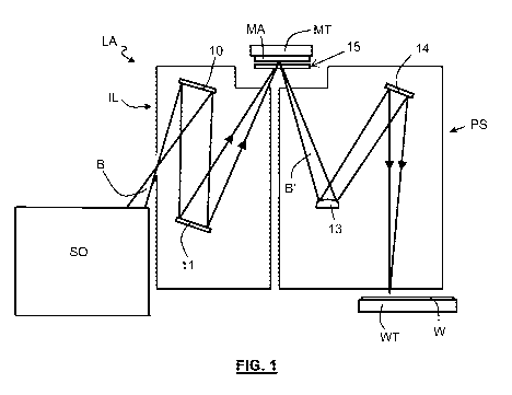
[00078] Figure 1
shows a lithographic system including a pellicle 15 according to the second,
fourth,
fifth and seventh aspects of the present invention or manufactured according
to the methods of the first
or third aspects of the present invention according to one embodiment of the
invention. The lithographic
CA 03099013 2020-11-02
WO 2019/211083
PCT/EP2019/059477
12
system comprises a radiation source SO and a lithographic apparatus LA. The
radiation source SO is
configured to generate an extreme ultraviolet (EUV) radiation beam B. The
lithographic apparatus LA
comprises an illumination system IL, a support structure MT configured to
support a patterning device
MA (e.g. a mask), a projection system PS and a substrate table WT configured
to support a substrate
W. The illumination system IL is configured to condition the radiation beam B
before it is incident
upon the patterning device MA. The projection system is configured to project
the radiation beam B
(now patterned by the mask MA) onto the substrate W. The substrate W may
include previously formed
patterns. Where this is the case, the lithographic apparatus aligns the
patterned radiation beam B with
a pattern previously formed on the substrate W. In this embodiment, the
pellicle 15 is depicted in the
path of the radiation and protecting the patterning device MA. It will be
appreciated that the pellicle 15
may be located in any required position and may be used to protect any of the
mirrors in the lithographic
apparatus.
[00079] The radiation source SO, illumination system IL, and projection
system PS may all be
constructed and arranged such that they can be isolated from the external
environment. A gas at a
pressure below atmospheric pressure (e.g. hydrogen) may be provided in the
radiation source SO. A
vacuum may be provided in illumination system IL and/or the projection system
PS. A small amount
of gas (e.g. hydrogen) at a pressure well below atmospheric pressure may be
provided in the
illumination system IL and/or the projection system PS.
[00080] The radiation source SO shown in Figure 1 is of a type which may
be referred to as a laser produced plasma (LPP) source). A laser which may for
example be a CO2 laser,
is arranged to deposit energy via a laser beam into a fuel, such as tin (Sn)
which is provided from a fuel
emitter. Although tin is referred to in the following description, any
suitable fuel may be used. The
fuel may for example be in liquid form, and may for example be a metal or
alloy. The fuel emitter may
comprise a nozzle configured to direct tin, e.g. in the form of droplets,
along a trajectory towards a
plasma formation region. The laser beam is incident upon the tin at the plasma
formation region. The
deposition of laser energy into the tin creates a plasma at the plasma
formation region. Radiation,
including EUV radiation, is emitted from the plasma during de-excitation and
recombination of ions of
the plasma.
[00081] The EUV radiation is collected and focused by a near normal
incidence radiation collector
(sometimes referred to more generally as a normal incidence radiation
collector). The collector may
have a multilayer structure which is arranged to reflect EUV radiation (e.g.
EUV radiation having a
desired wavelength such as 13.5 nm). The collector may have an elliptical
configuration, having two
ellipse focal points. A first focal point may be at the plasma formation
region, and a second focal point
may be at an intermediate focus, as discussed below.
[00082] The laser may be separated from the radiation source SO. Where this
is the case, the laser
beam may be passed from the laser to the radiation source SO with the aid of a
beam delivery system
CA 03099013 2020-11-02
WO 2019/211083
PCT/EP2019/059477
13
(not shown) comprising, for example, suitable directing mirrors and/or a beam
expander, and/or other
optics. The laser and the radiation source SO may together be considered to be
a radiation system.
[00083] Radiation that is reflected by the collector forms a radiation
beam
B. The radiation beam B is focused at a point to form an image of the plasma
formation region, which
acts as a virtual radiation source for the illumination system IL. The point
at which the radiation beam
B is focused may be referred to as the intermediate focus. The radiation
source SO is arranged such
that the intermediate focus is located at or near to an opening in an
enclosing structure of the radiation
source.
[00084] The radiation beam B passes from the radiation source SO into
the illumination system IL,
which is configured to condition the radiation beam. The illumination system
IL may include a facetted
field mirror device 10 and a facetted pupil mirror device 11. The faceted
field mirror device 10 and
faceted pupil mirror device 11 together provide the radiation beam B with a
desired cross-sectional
shape and a desired angular distribution. The radiation beam B passes from the
illumination system IL
and is incident upon the patterning device MA held by the support structure
MT. The patterning device
MA reflects and patterns the radiation beam B. The illumination system IL may
include other mirrors
or devices in addition to or instead of the faceted field mirror device 10 and
faceted pupil mirror device
11.
[00085] Following reflection from the patterning device MA the patterned
radiation beam B enters
the projection system PS. The projection system comprises a plurality of
mirrors 13, 14 which are
configured to project the radiation beam B onto a substrate W held by the
substrate table WT. The
projection system PS may apply a reduction factor to the radiation beam,
forming an image with features
that are smaller than corresponding features on the patterning device MA. A
reduction factor of 4 may
for example be applied. Although the projection system PS has two mirrors 13,
14 in Figure 1, the
projection system may include any number of mirrors (e.g. six mirrors).
[00086] The radiation sources SO shown in Figure 1 may include components
which are not
illustrated. For example, a spectral filter may be provided in the radiation
source. The spectral filter
may be substantially transmissive for EUV radiation but substantially blocking
for other wavelengths
of radiation such as infrared radiation.
[00087] Figure 2a shows a schematic depiction of a cross-section of
pellicle produced according to
the prior art methods. In this figure, the silicon support has already been
etched away to leave a border
18 and wafer remains 19 separated by a scribeline 16. The scribeline 16 is
bridged by the capping layer
17. As such, in order to release the border 18 from the wafer remains 19, it
is necessary to break or cut
the capping layer 17 bridging the scribeline 16, which can result in the
production of unwanted particles
which may contaminate the capping layer 17.
[00088] Figure 2b shows a schematic plan view of the pellicle shown in
Figure 2a. The border 18
is shown in phantom lines inboard of the scribeline 16. It will be appreciated
that the scribeline 16
would not be visible due to the presence of the capping layer 17, but the
scribeline 16 is shown for
CA 03099013 2020-11-02
WO 2019/211083
PCT/EP2019/059477
14
reasons of clarity. The border 18 of the silicon wafer acts as a frame around
the capping material 17 in
order to support the capping material 17 when in use as a pellicle.
[00089]
Figure 3a depicts a wafer according to the present invention comprising a
wafer 23, a
capping layer (the at least one layer) 17, scribeline 16, and mask 20. The
capping layer 17 is continuous
across the surface of the wafer 23 and the mask 20 on the opposite side of the
wafer 23 defines scribeline
16. The capping layer 17 may comprise a metal nitride layer (not shown). The
capping layer 17 may
comprise a metallic layer and a metal nitride layer disposed between the
metallic layer and the wafer
23. As described above, the presence of a metal nitride layer has been
surprisingly found to have a
number of benefits.
1 0
[00090] Figure 3b depicts the wafer after a portion 27 of the capping layer
17 overlying the
scribeline 16 has been removed. Arrows 21 indicate how at least a portion of
the gap 27 in the capping
layer 17 overlie at least a portion of the scribeline 16.
[00091]
In Figure 3c, a protective layer 22 has been applied to the wafer and the
wafer 23 has been
etched away in the places not protected by mask 20. The etching process does
not remove the protective
1 5 layer 22. Crucially, there is no capping material 17 bridging the
scribeline 16.
[00092]
As shown in Figure 3c, the protective layer 22 may have a projecting part 28,
which extends
into the gap 27.
[00093]
In Figure 3d, the protective layer 22 has been removed and the excess material
has been
removed in order to arrive at a pellicle. The remaining material from the
wafer 23 serves as a frame to
20
support the capping material 17 when in use as a pellicle. It will be
appreciated that the figures are not
to scale and are merely used to illustrate the different layers in the
pellicle rather than their respective
dimensions.
[00094]
Figure 4 depicts a schematic view of a pellicle according to the prior art.
The core material
comprises a wafer 23 core that is capped by native oxide layers 24. When the
capping layer 25 is
25 deposited onto the wafer, the native oxide layer 24 is between the core
23 and the capping layer 25.
[00095]
Figure 5a depicts the same wafer as shown in Figure 4, but the native oxide
layer is removed
from the wafer 23 inside a non-oxidising atmosphere or a vacuum 26. The
capping layer is deposited
onto the core whilst still in the non-oxidising atmosphere or vacuum 26, which
results in a pellicle
which does not comprise a native oxide layer. A metal nitride layer (not
shown) may be provided on
30 the
core layer once the native oxide layer has been removed. A metallic capping
layer may subsequently
be provided on the metal nitride layer. The metal nitride layer and the
metallic layer may comprise any
of the metals described in respect of any aspect of the present invention.
[00096]
Figure 5b is similar to Figure 5a, but depicts the case where the native oxide
layers 24 are
removed and the wafer 23 is thinned down, thereby resulting in a pellicle
which is thinner and has better
35
transmissivity than existing pellicles. The capping layer 25 is deposited
after the native oxide layer has
been removed and/or when the pellicle core has been thinned down. Again, a
metal nitride layer may
be provided once the native oxide layer has been removed and/or the pellicle
core has been thinned
CA 03099013 2020-11-02
WO 2019/211083
PCT/EP2019/059477
down. In this way, there may be a metal nitride layer provided between the
wafer 23 and the capping
layer 25. The removal of the native oxide layer and a portion of the pellicle
core and the subsequent
deposition of the capping layer is carried out within a non-oxidizing
environment.
[00097] Embodiments of the invention may also be described as worded in
the following clauses:
5 1) A wafer comprising a mask on one face and at least one layer on the
opposite face, wherein the mask
comprises at least one scribeline which overlies at least a portion of the
opposite face which is
substantially free of the at least one layer.
2) A wafer according to clause 1, wherein the wafer comprises silicon.
3) A wafer according to clause 1 or 2, wherein the mask comprises a positive
or a negative resist.
10 4) A wafer according to any of clauses 1 to 3, wherein the at least one
layer comprises one or more of
a membrane, a sacrificial layer, and a pellicle layer.
5) A wafer according to clause 4, wherein the pellicle layer comprises at
least one of a metallic layer,
an oxide layer, a nitride layer, a silicide layer, a semi-metallic layer, a
non-metallic layer, and a metal
nitride layer, optionally wherein the metallic layer and/or the metal nitride
layer comprises ruthenium,
15 molybdenum, boron, zirconium, titanium, tantalum, or combinations
thereof.
6) A wafer according to any of clauses 1 to 5, wherein the wafer further
comprises a protective layer.
7) A wafer according to clause 6, wherein the protective layer is arranged
over the at least one layer,
the at least one layer being arranged between the protective layer and the
mask.
8) A wafer according to clause 7, wherein the protective layer has a
projecting part extending into a
gap formed in the at least one layer at the location where said portion of the
opposite face is substantially
free of the at least one layer.
9) A wafer according to any of clauses 6-8, wherein the protective layer
comprises at least one of a
polymer, a resist, and a lacquer, preferably wherein the polymer is poly (p-
xylylene).
10) An assembly, comprising a wafer, a mask provided on one face of the wafer,
and at least one layer
provided on the opposite face of the wafer, wherein the mask comprises at
least one scribeline which
overlies at least a portion of the opposite face which is substantially free
of the at least one layer.
11) An assembly according to clause 10, wherein the wafer comprises silicon.
12) An assembly according to clause 10 or 11, wherein the mask comprises a
positive or a negative
resist.
13) An assembly according to any of clauses 10 to 12, wherein the at least one
layer comprises one or
more of a membrane, a sacrificial layer, and a pellicle layer.
14) An assembly according to clause 13, wherein the pellicle layer comprises
at least one of a metallic
layer, an oxide layer, a nitride layer, a silicide layer, a semi-metallic
layer, a non-metallic layer, and a
metal nitride layer, optionally wherein the metallic layer and/or the metal
nitride layer comprises
ruthenium, molybdenum, boron, zirconium, titanium, tantalum, or combinations
thereof.
15) An assembly according to any of clauses 10 to 14, wherein the assembly
further comprises a
protective layer.
CA 03099013 2020-11-02
WO 2019/211083
PCT/EP2019/059477
16
16) An assembly according to clause 15, wherein the at least one layer is
arranged between the
protective layer and the wafer.
17) An assembly according to clause 16, wherein the protective layer has a
projecting part extending
into a gap formed in the at least one layer at the said portion of the
opposite face which is substantially
free of the at least one layer.
18) An assembly according to any of clauses 10-18, wherein the protective
layer comprises at least one
of a polymer, a resist, and a lacquer, preferably wherein the polymer is poly
(p-xylylene).
19) A method of preparing a pellicle comprising the steps of: providing a
wafer comprising a mask on
one face and at least one layer on the opposite face, defining a scribeline in
the mask, and selectively
removing a portion of the at least one layer which at least partially overlies
the scribeline.
20) The method according to clause 19, wherein the method further comprises
providing a protective
layer over at least a portion of the at least one layer.
21) The method according to clause 19, wherein the method further comprises
providing a protective
layer over at least a portion of the at least one layer such that said at
least a portion of the at least one
1 5 .. layer is arranged between the protective layer and the mask.
22) The method according to clause 20 or 21, wherein the protective layer is
provided with a projecting
part extending into a gap formed by said selectively removed portion of the at
least one layer.
23) The method according to any of clauses 19 to 22, the method further
comprising etching at least a
portion of the wafer.
24) The method according to clause 23, the method further comprising removing
at least a portion of
the protective layer.
25) The method according to any of clauses 19 to 24, wherein the scribeline
and/or the mask is defined
by lithography.
26) The method according to any of clauses 19 to 25, wherein the at least one
layer comprises one or
more of a membrane, a sacrificial layer, and a pellicle layer.
27) The method according to any of clauses 23 to 26, wherein the etching is
dry etching, wet etching,
or a combination of the two.
28) The method according to any of clauses 19 to 27, wherein the protective
layer comprises at least
one of a polymer, a resist, and a lacquer.
29) The method according to clause 28, wherein the protective layer comprises
poly (p-xylylene).
30) A method of preparing a pellicle comprising the steps of: providing a
pellicle core, and removing
at least some material from at least one face of the pellicle core in a non-
oxidising environment.
31) A method according to clause 30, wherein the method further comprises
depositing a capping layer
on at least one face of the pellicle, optionally wherein the capping layer
comprises a metal nitride layer
and/or a metallic layer.
32) A method according to clause 30 or 31, wherein the material is removed by
etching.
CA 03099013 2020-11-02
WO 2019/211083
PCT/EP2019/059477
17
33) A method according to clause 32, wherein the etching is dry etching, wet
etching, or a combination
of the two.
34) A method according to clause 32 or 33, wherein the etching is effected by
directing a beam of ions
of a noble gas onto the surface of the pellicle core.
35) A method according to any of clauses 31 to 34, wherein the capping layer
is deposited under
vacuum.
36) A method according to any of clauses 30 to 35, wherein the non-oxidising
environment is a vacuum.
37) A pellicle for a lithographic apparatus comprising a silicon core and one
or more capping layers,
wherein the pellicle is substantially devoid of an oxide layer between the
silicon core and the one or
more capping layers.
38) A pellicle for a lithographic apparatus manufactured from or comprising a
wafer according to any
of clauses 1 to 9 or an assembly according to any of clauses 10-18 or clause
37, or according to the
methods of clauses 19 to 36.
39) Use of a pellicle manufactured according to the methods of clauses 19 to
36 or according to any of
clauses 1 to 18 or 37 in a lithographic apparatus.
40) A pellicle for a lithographic apparatus, wherein said pellicle comprises
at least one metal nitride
layer.
41) A pellicle according to clause 40, wherein the at least one metal nitride
layer comprises at least one
of titanium nitride and tantalum nitride.
[00098] While
specific embodiments of the invention have been described above, it will be
appreciated that the invention may be practiced otherwise than as described.
The descriptions above are
intended to be illustrative, not limiting. Thus it will be apparent to one
skilled in the art that
modifications may be made to the invention as described without departing from
the scope of the claims
set out below.