Note: Descriptions are shown in the official language in which they were submitted.
1
SOLID STATE LIGHTING DEVICE PROVIDING SPECTRAL POWER
DISTRIBUTION WITH ENHANCED PERCEIVED BRIGHTNESS
CROSS-REFERENCE TO RELATED APPLICATIONS
[0001] This
application claims priority to U.S. Patent Application No.
15/972,152 filed on May 5, 2018.
Technical Field
[0002] The present
disclosure relates to solid state lighting devices,
including devices with lumiphors arranged to be stimulated by electrically
activated solid state emitters, and relates to associated methods of making
and
using such devices.
Background
[0003] Solid-
state lighting devices such as light-emitting diodes (LEDs) are
increasingly used in both consumer and commercial applications.
Advancements in LED technology have resulted in highly efficient and
mechanically robust light sources with a long service life. Accordingly,
modern
LEDs have enabled a variety of new display applications and are being
increasingly utilized for general illumination applications, often replacing
incandescent and fluorescent light sources.
[0004] LEDs are
solid-state devices that convert electrical energy to light
and generally include one or more active layers of semiconductor material (or
an active region) arranged between oppositely doped n-type and p-type layers.
When a bias is applied across the doped layers, holes and electrons are
injected into the one or more active layers where they recombine to generate
emissions such as visible light or ultraviolet emissions. An LED chip
typically
includes an active region that may be fabricated, for example, from silicon
carbide, gallium nitride, gallium phosphide, aluminum nitride, gallium
arsenide-
based materials, and/or from organic semiconductor materials.
[0005] Solid
state emitters may include lumiphoric materials (also known as
lumiphors) that absorb a portion of emissions having a first peak wavelength
emitted by the emitter and re-emit light having a second peak
Date Recue/Date Received 2021-02-04
CA 03099124 2020-11-02
WO 2019/217238
PCT/US2019/030626
2
wavelength that differs from the first peak wavelength. Phosphors,
scintillators, and lumiphoric inks are common lumiphoric materials. Light
perceived as white or near-white may be generated by a combination of red,
green, and blue ("RGB") emitters, or, alternatively, by combined emissions of
a blue LED and a lumiphor such as a yellow phosphor (e.g., YAG:Ce or
Ce:YAG). In the latter case, a portion of the blue LED emissions pass
through the phosphor, while another portion of the blue emissions is
downconverted to yellow, and the blue and yellow light in combination are
perceived as white. White light may also be produced by stimulating
phosphors or dyes of multiple colors with a violet or UV LED source.
[0006] Emissions of
a blue LED in combination with a yellow or green
lumiphoric material may be near-white in character and referred to as "blue-
shifted yellow" ("BSY") light or ''blue-shifted green" ('BSG") light. Addition
of
red (or red-orange) spectral output from a red-emitting LED (to yield a
"BSY+R" device) or from a red lumiphoric material (to yield a "BS(Y+R)"
device) may be used to increase the warmth of the aggregated light output
and better approximate light produced by incandescent lamps.
[0007] Color
reproduction is commonly measured using Color Rendering
Index (CRI) or average Color Rendering Index (CRI Ra). To calculate CRI,
the color appearance of 14 reflective samples is simulated when illuminated
by a reference radiator (illuminant) and the test source. The general or
average color rendering index CRI Ra is a modified average utilizing the first
eight indices, all of which have low to moderate chromatic saturation. (R9 is
one of six saturated test colors not used in calculating CRI, with R9
embodying a large red content.) CRI and CRI Ra are used to determine how
closely an artificial light source matches the color rendering of a natural
light
source at the same correlated color temperature. Daylight has a high CRI Ra
(approximately 100), with incandescent bulbs also being relatively close (CRI
Ra greater than 95), and fluorescent lighting being less accurate (with
typical
CRI Ra values of approximately 70-80).
[0008] The reference
spectra used in color rendering index calculations
were chosen as ideal illumination sources defined in terms of their color
temperature. As a heated object becomes incandescent, it first glows
CA 03099124 2020-11-02
WO 2019/217238
PCT/US2019/030626
3
reddish, then yellowish, then white, and finally bluish. Thus, apparent colors
of
incandescing materials are directly related to their actual temperature (in
Kelvin (K). Practical materials that incandesce are said to have correlated
color temperature (CCT) values that are directly related to color temperatures
of blackbody sources.
[0009] Aspects relating to the inventive subject matter disclosed herein
may be better understood with reference to the 1931 CIE (Commission
International de l'Eclairage) Chromaticity Diagram, which is well-known and of
which a copy is reproduced in FIG. 1. The 1931 CIE Chromaticity Diagram
maps out the human color perception in terms of two CIE parameters x and y.
The spectral colors are distributed around the edge of the outlined space,
which includes all of the hues perceived by the human eye. The boundary line
represents maximum saturation for the spectral colors. The chromaticity
coordinates (i.e., color points) that lie along the blackbody locus ("BBL")
(also
known as the Planckian locus) obey Planck's equation: E(A)=A5/(eB/T_i
where E is the emission intensity, A is the emission wavelength, T the color
temperature of the blackbody, and A and B are constants. Color coordinates
that lie on or near the blackbody locus (which embodies a curved line
emanating from the right lower corner) yield pleasing white light to a human
.. observer. The 1 931 CIE Diagram includes temperature listings along the
blackbody locus, with these temperature listings showing the color path of a
blackbody radiator that is caused to increase to such temperatures. As a
heated object becomes incandescent, it first glows reddish, then yellowish,
then white, and finally bluish. This occurs because the wavelength associated
with the peak radiation of the blackbody radiator becomes progressively
shorter with increased temperature, consistent with the Wien Displacement
Law. Illuminants which produce light that is on or near the blackbody locus
can thus be described in terms of their color temperature. The white area
proximate to (i.e., within approximately a MacAdam eight-step ellipse of) of
the BBL and between 2,500 K and 10,000 K, is shown in FIG. 1.
[0010] The term "white light" or "whiteness" does not clearly cover the
full
range of colors along the BBL since it is apparent that a candle flame and
other incandescent sources appear yellowish, i.e., not completely white.
CA 03099124 2020-11-02
WO 2019/217238
PCT/US2019/030626
4
Accordingly, the color of illumination may be better defined in terms of
correlated color temperature (COT) and in terms of its proximity to the BBL.
The pleasantness and quality of white illumination decreases rapidly if the
chromaticity point of the illumination source deviates from the BBL by a
distance of greater than 0.01 in the x, y chromaticity system. This
corresponds
to the distance of about a MacAdam four-step ellipse, a standard employed by
the lighting industry. A lighting device emitting light having color
coordinates
that are within a MacAdam four-step ellipse of the BBL and that has a CRI
Ra>80 is generally acceptable as a white light for general illumination
purposes. A lighting device emitting light having color coordinates within a
MacAdam seven- or eight-step ellipse of the BBL and that has a CRI Ra>70 is
used as the minimum standards for many other white lighting devices
including compact fluorescent and solid state lighting devices. FIG. 2
illustrates MacAdam 2-step, 4-step, and 7-step ellipses for a CCT of 3200K
relative to a segment of the BBL (e.g., extending generally between 2900K
and 3500K).
[0011] Quality artificial lighting generally attempts to emulate the
characteristics of natural light. Natural light sources include daylight with
a
relatively high color temperature (e.g., -5000K) and incandescent lamps with
.. a lower color temperature (e.g., -2800K). General illumination generally
has
a color temperature between 2,000 K and 10,000 K, with the majority of
lighting devices for general illumination being between 2,700 K and 6,500 K.
The white area proximate to (i.e., within approximately a MacAdam eight-step
ellipse of) of the BBL and between 2,500 K and 10,000 K, is shown in FIG. 1.
[0001] Luminous efficacy is a measure of how well a light source
produces visible light, and represents the ratio of luminous flux to power
(with
the power being either radiant flux or total power consumed by a source,
depending on the context). Wavelengths of light outside of the visible
spectrum are not useful for illumination because they cannot be seen by the
human eye. Moreover, the human eye exhibits greater response to some
wavelengths of light than to others, even within the visible spectrum.
Response of the human eye to light also varies with respect to the level of
intensity of light.
CA 03099124 2020-11-02
WO 2019/217238
PCT/US2019/030626
[0002] At the back of the eye, the retina contains millions of light
receptors
that convert light into electrified signals that are sent to vision centers of
the
brain. The retina contains two major categories of photoreceptors called
cones and rods because of their geometric shapes. The very central part of
5 the retina, called the fovea, contains only cones. The rest of the retina
is
populated with both rods and cones, with the number of rods exceeding the
number of cones by a ratio of about 10 to 1.
[0012] Three visual states that depend on the level of illuminance are
photopic vision, scotopic vision, and mesoptic vision. Photopic vision is the
.. vision of the eye under well-lit conditions. In humans and many other
animals, photopic vision is mediated by cone cells, and allows color
perception and significantly higher visual acuity than available with scotopic
vision. The human eye uses three types of cones (with biological pigments
having maximum absorption values at wavelengths of about 420 nm (blue),
534 nm (bluish-green), and 564 nm (yellowish green)) to sense light in three
bands of color, providing maximum efficacy of about 683 ImNV at a
wavelength of 555 nm (in the green-yellow part of the visible light spectrum).
Scotopic vision is the vision of the eye under very low light (e.g., nearly
dark)
conditions, in which much color discernment is lost. In the human eye, cone
cells are nonfunctional in low light; as a result, scotopic vision is produced
exclusively through rod cells, which are most sensitive to wavelengths of
light
around 498 nm (green-blue) and are not sensitive to wavelengths longer than
about 640 nm (red). Mesoptic vision occurs at illuminance levels between
those of photopic and scotopic vision. In particular, scotopic vision occurs
at
.. luminance levels of 10-2 to 10-6 cd/m2; photopic vision occurs at luminance
levels of 1 to 106 cd/m2 (normal light); and mesopic vision occurs in
intermediate lighting conditions (luminance levels of 10-2 to 1 cd/m2).
Mesoptic vision is effectively a combination of scotopic and photopic vision,
but yields less accurate visual acuity and color discrimination.
[0013] FIG. 3 illustrates scotopic and photopic luminosity functions, with
the leftmost curve embodying a scotopic luminosity function (as adopted by
the Commission Internationale de l'Eclairage (CIE) in 1951), and with the
rightmost curve embodying a photopic luminosity functions (wherein the solid
CA 03099124 2020-11-02
WO 2019/217238
PCT/US2019/030626
6
line represents the CIE 1931 standard). The CIE 1931 photopic luminosity
function also forms the central color matching function in the CIE 1931 color
space. As shown in FIG. 3, the scotopic curve exhibits significant response
above 420 nm, a peak at 507 nm, and very little response above 600 nm,
whereas the photopic curve exhibits very limited response below 450 nm, a
peak at 555 nm, and still-significant response above 650 nm before declining
to zero response around 700 nm. For everyday light levels, the photopic
luminosity function best approximates the response of the human eye;
however, for low light levels, the response of the human eye changes, and the
scotopic luminosity function applies. This difference in the scotopic and
photopic luminous efficacy of the source results from the shift of eye
sensitivity function peaking at 555nm (under photopic lighting conditions) to
507nm (under scotopic lighting conditions), also known as the Purkinje shift.
[0014] Historically,
lighting manufacturers have utilized light meters to
determine a lamp's lumen output that are calibrated by examining the eye's
sensitivity to only cone activated vision in the very central part of the
retina,
the fovea, while ignoring the effect of rod activated vision. As a result,
traditional lighting practice accepted a single sensitivity function based on
the
assumption that the more light sensitive rods only functioned at very dim
light
levels. More recent studies have demonstrated that rod photoreceptors are
active not only in dim light but also at typical interior light levels as
well.
[0015] Since rods
are more sensitive than cones to bluish-white light
sources characteristic of higher correlated color temperature (COT) values, an
environment lit with a light source having a higher OCT value (e.g., 5000K or
above) may appear brighter than the same environment lit with a light source
having a lower COT value (e.g., warm white (3000K) and cool white (4100K)
lamps such as fluorescent tubes). Light having a higher COT value yields
relatively smaller pupils at a given photopic light level, so that object
light rays
are collected more at the central region of the eye, which may result in
improved optical vision. Despite this,
adjustment of COT alone is not
sufficient to optimize human-perceived brightness in a given environment.
Moreover, light having moderately to very high CCT values may not be
pleasing to some observers.
CA 03099124 2020-11-02
WO 2019/217238
PCT/US2019/030626
7
[0016] It has been recently recognized that photosensitive retinal
ganglion
cells expressing the photopigment melanopsin is involved not only in circadian
photoentrainment, but also in perceived brightness of light. Melanopsin
photoreceptors are sensitive to a range of wavelengths and reach peak light
absorption at blue light wavelengths around 480 nm. A "melanopic" spectral
efficiency function has been determined to predict the sensitivity of
melanopsin photoreceptors to polychromatic lights.
[0017] Despite the potential for increasing perceived brightness using
lamps with increased melanopic content (e.g., spectral content at or near 480
nm), it is not straightforward to make such a light source with sufficient
levels
of color rendering (e.g., to enable color differentiation).
[0018] Accordingly, the art continues to seek improved solid state
lighting
devices that provide desirable illumination characteristics and are capable of
overcoming challenges associated with conventional lighting devices.
Summary
[0019] The present disclosure relates in various aspects to solid state
(e.g., LED) lighting devices including at least one electrically activated
(e.g.,
blue light emitting) solid state light emitter configured to stimulate
emissions of
multiple lumiphoric materials having different peak wavelengths, with the
lighting device providing aggregated emissions having a suitably high color
rendering index (e.g., CRI Ra) value (e.g., at least 70, 80, 85, or 90 in
certain
embodiments), and also having a spectral power distribution with a
Melanopic/Photopic ratio (M/P ratio) within a specified target range as a
function of correlated color temperature. At least one lumiphoric material
includes a relatively narrow peak width (e.g., expressed in terms of a full
width
half maximum value or "FWHM"). The specified M/P ratio target range is
believed to be greater than attained with conventional lighting devices
including multiple lumiphoric materials stimulated by at least one blue solid
state light emitter.
[0020] In one aspect, the present disclosure relates to a lighting device
including at least one electrically activated solid state light emitter
arranged to
generate emissions having a peak wavelength in a blue range; and first
CA 03099124 2020-11-02
WO 2019/217238
PCT/US2019/030626
8
through third lumiphoric materials arranged to receive at least a portion of
emissions of the at least one electrically activated solid state light emitter
and
configured to responsively generate lumiphor emissions. Lumiphor emissions
of the first through third lumiphoric materials have peak wavelengths in three
ranges. In particular, lumiphor emissions of the first lumiphoric material
have
a first peak wavelength in a range of from 485 nm to 530 nm (or a subrange
thereof specified herein); lumiphor emissions of the second lumiphoric
material have a second peak wavelength in a range of from 575 nm to 612 nm
(or a subrange thereof specified herein); and lumiphor emissions of the third
.. lumiphoric material having a third peak wavelength in a range of from 605
nm
to 640 nm (or a subrange thereof specified herein). The third peak
wavelength further corresponds to a third peak having a full width half
maximum value of less than 60 nm (or less than 35 nm in certain
embodiments). Aggregated emissions of the lighting device include emissions
.. of the at least one electrically activated solid state light emitter as
well as the
first through third lumiphoric materials. Aggregated emissions of the lighting
device have a CRI Ra value of at least 70 (or another threshold specified
herein), and also have a spectral power distribution with a Melanopic/Photopic
ratio (M/P ratio) value within a target range as a function of correlated
color
temperature (COT) in Kelvin. The target range includes minimum values
defined by a minimum value function in which M/P ratio equals [-2.05x10-
8(CCT)2 + 2.72x10⁻⁴(CCT) ¨ 0.1506]. Preferably, the target range also
includes maximum values defined by a maximum value function in which M/P
ratio equals [-2.57x10⁻⁸(CCT)2 + 3.70x10⁻⁴(CCT) - 0.1889], and COT being in
a range of from 2000 to 7000 Kelvin.
[0021] In certain embodiments, the lighting device includes aggregated
emissions having a spectral power distribution with a Melanopic/Photopic ratio
(M/P ratio) value within a first target subrange as a function of CCT in
Kelvin
of the aggregated emissions, the first target subrange including minimum
values defined by a minimum value function in which M/P ratio equals [-
2.05x10⁻⁸(CCT)2 + 2.72x10⁻⁴(CCT) ¨ 0.1506]the first target subrange
including maximum values defined by a maximum value function in which M/P
CA 03099124 2020-11-02
WO 2019/217238
PCT/US2019/030626
9
ratio equals [-2.57x10⁻⁸(CCT)2 + 3.70x10⁻⁴(CCT) - 0.1889], and COT being in
a range of from 2000 to 7000 Kelvin.
[0022] In certain embodiments, the lighting device includes aggregated
emissions having a spectral power distribution with a Melanopic/Photopic ratio
(M/P ratio) value within a second target subrange as a function of CCT in
Kelvin of the aggregated emissions, the second target subrange including
minimum values defined by a minimum value function in which M/P ratio
equals [-2.05x10⁻⁸(CCT)2 + 2.72x10⁻⁴(CCT) ¨ 0.1506]the second target
subrange including maximum values defined by a maximum value function in
which M/P ratio equals [-2.57x10⁻⁸(CCT)2 + 3.70x10⁻⁴(CCT) - 0.1889]and COT
being in a range of from 2000 to 7000 Kelvin.
[0023] In certain embodiments, a COT value of the aggregated emissions
is in a range of from 2000 to 6000 Kelvin.
[0024] In certain embodiments, the second peak wavelength (i.e., in a
range of from 575 nm to 612 nm, or a subrange of from 575 nm to 595 nm, or
a subrange of from 580 nm to 590 nm, or any subrange thereof disclosed
herein) corresponds to a second peak having a full width half maximum value
of less than 60 nm (or less than 35 nm in certain embodiments).
[0025] In certain embodiments, the aggregated emissions define a color
point within a 10 step MacAdam ellipse (or within a 7step MacAdam ellipse)
of a Planckian Locus on a CIE 1931 chromaticity diagram.
[0026] In certain embodiments, the at least one electrically activated
solid
state light emitter has a peak wavelength in a range of from 430 nm to 480
nm, or within a range of from 440 nm to 460 nm.
[0027] In certain embodiments, the at least one electrically activated
solid
state light emitter comprises a plurality of electrically activated solid
state light
emitters.
[0028] In certain embodiments, lumiphor emissions of the first lumiphoric
material have a first peak wavelength in a subrange of from 490 nm to 500
nm. In certain embodiments, lumiphor emissions of the second lumiphoric
material have a second peak wavelength in a subrange of from 575 nm to 595
nm, or a subrange of from 580 nm to 590 nm. In certain embodiments,
lumiphor emissions of the third lumiphoric material have a third peak
CA 03099124 2020-11-02
WO 2019/217238
PCT/US2019/030626
wavelength is in a subrange of from 610 nm to 625 nm. In certain
embodiments, the third peak wavelength corresponds to a third peak having a
full width half maximum value of less than 35 nm.
[0029] In certain
embodiments, aggregated emissions of the lighting
5 device have a CRI Ra value of at least 80, or in a range of from 70 to
95, or in
a range of from 75 to 95, or in a range of from 70 to 90.
[0030] In certain
embodiments, the first through third lumiphoric materials
are dispersed in a binder. In certain
embodiments, the first lumiphoric
material is arranged in a first layer, the second lumiphoric material is
arranged
10 in a second layer, and the third lumiphoric material is arranged in a
third layer.
[0031] In another
aspect, the present disclosure relates to a lighting device
including at least one electrically activated solid state light emitter
arranged to
generate emissions having a peak wavelength in a blue range; at least one
supplemental electrically activated solid state light emitter; and a plurality
of
lumiphoric materials arranged to receive at least a portion of emissions of
the
at least one electrically activated solid state light emitter and configured
to
responsively generate lumiphor emissions. Aggregated emissions of the
lighting device include emissions of the at least one electrically activated
solid
state light emitter, emissions of the at least one supplemental electrically
activated solid state light emitter, and emissions of the plurality of
lumiphoric
materials. Aggregated emissions of the lighting device include a first peak
wavelength in a range of 430 nm to 480 nm, a second peak wavelength in a
range of from 485 nm to 530 nm, a third peak wavelength in a range of from
575 nm to 612 nm, and a fourth peak wavelength in a range of from 605 nm to
640 nm, and the fourth peak wavelength corresponds to a peak having a full
width half maximum value of less than 60 nm. Aggregated emissions of the
lighting device have a CRI Ra value of at least 70 (or another threshold
specified herein), and also have a spectral power distribution with a
Melanopic/Photopic ratio (M/P ratio) value within a target range as a function
of correlated color temperature (CCT) in Kelvin. The target range includes
minimum values defined by a minimum value function in which M/P ratio
equals [-2.05x10⁻⁸(CCT)2 + 2.72x10⁻⁴(CCT) ¨ 0.1506]. Preferably, the target
range also includes maximum values defined by a maximum value function in
11
which M/P ratio equals [-2.57x10⁻⁸(CCT)2+ 3.70x10⁻⁴(CCT)- 0.1889], and CCT
being in a range of from 2000 to 7000 Kelvin. In certain embodiments, the at
least one supplemental electrically activated solid state light emitter is
configured to generate the second peak wavelength or the fourth peak
wavelength. In certain embodiments, the second peak wavelength is in a
subrange of from 485 nm to 505 nm, the third peak wavelength is in a subrange
of from 575 nm to 595 nm.
[0032] In another aspect, the present disclosure relates to a method
comprising illuminating an object, a space, or an environment, utilizing a
solid
state lighting device as described herein.
[0033] In another aspect, any of the foregoing aspects, and/or various
separate aspects and features as described herein, may be combined for
additional advantage. Any of the various features and elements as disclosed
herein may be combined with one or more other disclosed features and
elements unless indicated to the contrary herein.
[0033a] In another aspect, there is a lighting device comprising: at least one
electrically activated solid state light emitter arranged to generate
emissions
having a peak wavelength in a blue range; and first through third lumiphoric
materials arranged to receive at least a portion of emissions of the at least
one
electrically activated solid state light emitter and configured to
responsively
generate lumiphor emissions; wherein: lumiphor emissions of the first
lumiphoric material have a first peak wavelength in a range of from 485 nm to
530 nm; lumiphor emissions of the second lumiphoric material have a second
peak wavelength in a range of from 575 nm to 612 nm; lumiphor emissions of
the third lumiphoric material having a third peak wavelength in a range of
from
605 nm to 640 nm, wherein the third peak wavelength corresponds to a third
peak having a full width half maximum value of less than 60 nm; aggregated
emissions of the lighting device include emissions of the at least one
electrically
activated solid state light emitter, the first lumiphoric material, the second
lumiphoric material, and the third lumiphoric material; aggregated emissions
of
the lighting device have an average Color Rendering Index (CRI Ra) value of
at least 70; and aggregated emissions of the lighting device have a spectral
power distribution with a Melanopic/Photopic ratio (M/P ratio) value within a
Date Recue/Date Received 2021-02-04
11a
target range as a function of correlated color temperature (CCT) in Kelvin of
the
aggregated emissions, the target range including minimum values defined by a
minimum value function in which the M/P ratio equals [-2.05x10⁻⁸(CCT)2 +
2.72x10⁴(CCT) ¨ 0.1506], and the target range including maximum values
defined by a maximum value function in which the M/P ratio equals [-2.57x10-
8(CCT)2+ 3.70x10⁴(CCT) - 0.1889], and the CCT being in a range of from 2000
Kelvin to 7000 Kelvin.
[0033b] In another aspect, there is a lighting device comprising: at least one
electrically activated solid state light emitter arranged to generate
emissions
having a peak wavelength in a blue range; and at least one supplemental
electrically activated solid state light emitter; and a plurality of
lumiphoric
materials arranged to receive at least a portion of emissions of the at least
one
electrically activated solid state light emitter and configured to
responsively
generate lumiphor emissions; wherein: aggregated emissions of the lighting
device include emissions of the at least one electrically activated solid
state
light emitter, emissions of the at least one supplemental electrically
activated
solid state light emitter, and emissions of the plurality of lumiphoric
materials;
the aggregated emissions include a first peak wavelength in a range of 430 nm
to 480 nm, a second peak wavelength in a range of from 485 nm to 530 nm, a
third peak wavelength in a range of from 575 nm to 612 nm, and a fourth peak
wavelength in a range of from 605 nm to 640 nm, and the fourth peak
wavelength corresponds to a peak having a full width half maximum value of
less than 60 nm; aggregated emissions of the lighting device have an average
Color Rendering Index (CRI Ra) value of at least 70; and aggregated emissions
of the lighting device have a spectral power distribution with a
Melanopic/Photopic ratio (M/P ratio) value within a target range as a function
of
correlated color temperature (CCT) in Kelvin of the aggregated emissions, the
target range including minimum values defined by a minimum value function in
which the M/P ratio equals [-2.05x10⁻⁸(CCT)2 + 2.72x10⁻⁴(CCT) ¨ 0.1506],
and the target range including maximum values defined by a maximum value
function in which the M/P ratio equals [-2.57x10⁻⁸(CCT)2 + 3.70x10⁻⁴(CCT) -
0.1889], and the CCT being in a range of from 2000 Kelvin to 7000 Kelvin.
[0034] Other aspects, features and embodiments of the present disclosure
will be more fully apparent from the ensuing disclosure and appended claims.
Date Recue/Date Received 2021-02-04
11 b
Brief Description of the Drawings
[0035] The accompanying drawing figures incorporated in and forming a
part of this specification illustrate several aspects of the disclosure, and
together with the description serve to explain the principles of the
disclosure.
[0036] FIG. 1 is a 1931 CIE Chromaticity Diagram with identification of a
white area proximate to (i.e., within approximately a MacAdam eight-step
ellipse of) of the blackbody or Planckian locus, and identification of
correlated
color temperature values ranging from 1,000 to 30,000 K.
[0037] FIG. 2 illustrates MacAdam 2-step, 4-step, and 7-step ellipses for a
CCT of 3200K relative to a segment of the BBL.
[0038] FIG. 3 provides plots of the scotopic and photopic luminosity
functions expressed in relative intensity versus wavelength.
[0039] FIG. 4 is a photograph of two side-by-side test booths subject to
being illuminated differently, with the booths being in a filled state
containing
colored objects.
Date Recue/Date Received 2021-02-04
CA 03099124 2020-11-02
WO 2019/217238
PCT/US2019/030626
12
[0040] FIG. 5 provides spectral power distribution plots (in normalized
intensity versus wavelength) for two light sources, namely: a high perceived
brightness ("High PB") light source (e.g., according to the third booth survey
described hereinafter), and a point of reference ("PoR") 70 CRI light source,
both at a CCT of 4000K and at 900Iux.
[0041] FIG. 6A is a table including results of first through fifth booth
surveys utilizing side-by-side illuminated booths to compare spectral outputs
of multiple purported high perceived brightness lumiphor converted LED-
based light sources (each including a different phosphor blend) to a 70 CRI
reference lumiphor converted LED light source.
[0042] FIG. 6B is a table identifying results of a sixth booth survey
utilizing
side-by-side illuminated booths to compare a 78 CRI LED-based light source
to an 80 CRI reference lumiphor converted LED light source.
[0043] FIG. 7A provides spectral power distribution plots (in normalized
intensity versus wavelength) for four light sources and the reference light
source utilized in the first, second, third, and fifth surveys described in
connection with FIG. 6A.
[0044] FIG. 7B provides the same image as FIG. 7A, with addition of
normalized melanopic and normalized photopic spectral power distribution
plots.
[0045] FIG. 8 is a plot of perceived brightness gain versus
melanopic/photopic spectral ratio for the light sources utilized in the first
through fifth booth surveys described in connection with FIG. 6A.
[0046] FIG. 9 provides plots and superimposed curvefits of
melanopic/photopic spectral ratio versus CCT for the first PoR 70 CRI light
source, for the light source used in the fifth booth survey, and for a modeled
High PB light source having at least 70 CRI, with addition of data points for
a
commercially available Soraa Vivid 95 CRI light source and for an artificial
skylight with a mid-day sun and sky setting.
[0047] FIG. 10A provides plots and superimposed curvef its of
melanopic/photopic spectral ratio versus CCT for two light sources at five
different positions relative to the blackbody locus (BBL), namely: on the BBL,
within a MacAdam 4 step ellipse above the BBL, within a MacAdam 4 step
CA 03099124 2020-11-02
WO 2019/217238
PCT/US2019/030626
13
ellipse below the BBL, within a MacAdam 2 step ellipse above the BBL, and
within a MacAdam 2 step ellipse below the BBL.
[0048] FIG. 10B provides a magnified view of a lower portion of FIG. 10A.
[0049] FIG. 10C provides a magnified view of an upper portion of FIG.
10A.
[0050] FIG. 11 shows color points for two light sources E2 2A and E2 2B
arranged below and above the BBL, respectively, at a CCT value of just
above 6000K, in a magnified portion of a 1931 CIE chromaticity diagram.
[0051] FIG. 12 provides spectral power distribution plots (in normalized
intensity versus wavelength) for the two light sources (namely, E2 2A and E2
2B) of FIG. 11, with a superimposed normalized melanopic spectral power
function plot.
[0052] FIG. 13 is a table identifying duv, CCT, CRI, and M/P ratio values
for two light sources E2 2A and E2 2B of FIGS. 11 and 12.
[0053] FIG. 14 is a schematic cross-sectional view of a first exemplary
light
emitting diode that may embody (or may be incorporated in) a lighting device
according to one embodiment of the present disclosure.
[0054] FIG. 15 is a schematic cross-sectional view of a second exemplary
light emitting diode that may embody (or may be incorporated in) a lighting
device according to one embodiment of the present disclosure.
[0055] FIG. 16A is a side cross-sectional schematic view of at least a
portion of a solid state light emitting device including a solid state emitter
chip
arranged over a package mount, with a top surface of the emitter chip being
covered with a wavelength conversion material.
[0056] FIG. 166 is a side cross-sectional schematic view of at least a
portion of a solid state light emitting device including the device of FIG.
16A
with addition of a curved (e.g., hemispherical) lens.
[0057] FIG. 17A is a side cross-sectional schematic view of at least a
portion of a solid state light emitting device including a solid state emitter
chip
arranged over a package mount, with top and side surfaces of the emitter chip
and an upper surface of the package mount being covered with a wavelength
conversion material.
CA 03099124 2020-11-02
WO 2019/217238
PCT/US2019/030626
14
[0058] FIG. 17B is a side cross-sectional schematic view of at least a
portion of a solid state light emitting device including the device of FIG.
17A
with addition of a lens having a substantially rectangular cross-sectional
shape.
[0059] FIG. 18A is a side cross-sectional schematic view of at least a
portion of a solid state light emitting device including a solid state emitter
chip
arranged over a package mount, with a top surface of the emitter chip being
covered with at least one wavelength conversion material layers.
[0060] FIG. 18B is a side cross-sectional schematic view of at least a
portion of a solid state light emitting device including the device of FIG.
18A
with addition of a curved (e.g., hemispherical) lens.
[0061] FIG. 19A is a side cross-sectional schematic view of at least a
portion of a solid state light emitting device including a solid state emitter
chip
arranged over a package mount, with top and side surfaces of the emitter chip
and an upper surface of the package mount being covered with multiple
wavelength conversion material layers.
[0062] FIG. 19B is a side cross-sectional schematic view of at least a
portion of a solid state light emitting device including the device of FIG.
19A
with addition of a lens having a substantially rectangular cross-sectional
shape.
[0063] FIG. 20 is a side cross-sectional view of at least a portion of a
solid
state light emitting device including multiple solid state emitter chips
coated
with multiple lumiphoric materials and arranged under a hemispherical optical
element.
[0064] FIG. 21 is a perspective view of at least a portion of a solid state
emitter package including multiple solid state emitter chips coated with
multiple lumiphoric materials, with the chips coupled to electrical traces via
wirebonds and arranged under a hemispherical optical element.
[0065] FIG. 22A is a side elevation view of a lighting device according
to
one embodiment of the disclosure embodied in a substantially cylindrical
downlight intended for in-ceiling mounting and including multiple LEDs.
[0066] FIG. 22B is a cross-sectional view of the lighting device of FIG.
22A.
CA 03099124 2020-11-02
WO 2019/217238 PCT/US2019/030626
[0067] FIG. 220 is an upper perspective view of the lighting device of
FIGS. 22A-22B.
[0068] FIG. 22D is a lower perspective view of the lighting device of
FIGS.
22A-22C.
5 [0069] FIG. 23A is an upper perspective view of a light bulb including
multiple LEDs arranged in a two-dimensional array according to one
embodiment of the disclosure.
[0070] FIG. 23B is a side elevation view of the light bulb of FIG. 23A.
[0071] FIG. 24A is an upper perspective view of a troffer-type light
fixture
10 arranged to incorporate multiple solid state emitters as disclosed
herein.
[0072] FIG. 24B is a side cross-sectional view of a portion of the light
fixture of FIG. 24A.
[0073] FIGS. 25A and 25B illustrate a high bay/low bay solid state
lighting
fixture including multiple solid state light emitters.
15 [0074] FIGS. 26A-26B illustrate a first outdoor floodlight fixture
including
multiple solid state light emitters.
[0075] FIGS. 27A-27B illustrate a second outdoor floodlight fixture
including multiple solid state light emitters.
Detailed Description
[0076] The embodiments set forth below represent the necessary
information to enable those skilled in the art to practice the embodiments and
illustrate the best mode of practicing the embodiments. Upon reading the
following description in light of the accompanying drawing figures, those
skilled in the art will understand the concepts of the disclosure and will
recognize applications of these concepts not particularly addressed herein. It
should be understood that these concepts and applications fall within the
scope of the disclosure and the accompanying claims.
[0077] As noted previously, the art continues to seek solid state
lighting
devices providing desirable illumination characteristics. Brightness of
illumination provided by a light source has traditionally focused on
measurement of lumen output, without accurately representing perceived
CA 03099124 2020-11-02
WO 2019/217238
PCT/US2019/030626
16
brightness in real-world settings taking into account perception of human
viewers.
[0078] Various embodiments disclosed herein relate to lighting devices
capable of providing light with enhanced perceived brightness, in combination
with acceptably light quality (e.g., color fidelity, which may be expressed as
CRI or CRI Ra). Perceived brightness may be enhanced by increasing
spectral content at or near the melanopic spectral efficiency peak of 480 nm,
while providing amber/orange-red or short wavelength red content (e.g.,
having a peak wavelength in a range of from 575 nm to 612 nm, or 575 nm to
595 nm, or 580 nm to 590 nm) in combination with narrow-band red content
(e.g., having a peak wavelength in a range of from 605 nm to 640 nm,
corresponding to a peak having a full width half maximum value of less than
60 nm (or less than 35 nm)) facilitate attainment of a desired color target
for
aggregated emissions and attainment of color quality requirements (e.g., CRI
Ra value of at least 70, or another threshold or range identified herein). Use
of at least one narrow-band emitting lumiphoric material may beneficially
increase perceived brightness and efficacy of aggregated emissions of a
lighting device.
[0079] In certain embodiments, one of the spectral peaks mentioned above
may be provided by a supplemental (e.g., cyan, green, amber/orange, or red)
electrically activated solid state light emitter (e.g., an LED) instead of a
lumiphoric material.
[0080] More specific aspects of the disclosure will be described after
terms
are defined and general concepts are introduced.
[0081] It will be understood that, although the terms first, second, etc.
may
be used herein to describe various elements, these elements should not be
limited by these terms. These terms are only used to distinguish one element
from another. For example, a first element could be termed a second
element, and, similarly, a second element could be termed a first element,
without departing from the scope of the present disclosure. As used herein,
the term "and/or" includes any and all combinations of one or more of the
associated listed items.
CA 03099124 2020-11-02
WO 2019/217238
PCT/US2019/030626
17
[0082] It will be understood that when an element such as a layer,
region,
or substrate is referred to as being "on" or extending "onto" another element,
it
can be directly on or extend directly onto the other element or intervening
elements may also be present. In contrast, when an element is referred to as
being "directly on' or extending "directly onto" another element, there are no
intervening elements present. Likewise, it will be understood that when an
element such as a layer, region, or substrate is referred to as being ''over"
or
extending "over" another element, it can be directly over or extend directly
over the other element or intervening elements may also be present. In
contrast, when an element is referred to as being "directly over" or extending
"directly over" another element, there are no intervening elements present. It
will also be understood that when an element is referred to as being
"connected" or "coupled" to another element, it can be directly connected or
coupled to the other element or intervening elements may be present. In
contrast, when an element is referred to as being "directly connected" or
"directly coupled" to another element, there are no intervening elements
present.
[0083] Relative terms such as "below" or "above" or "upper" or "lower" or
"horizontal" or "vertical" may be used herein to describe a relationship of
one
element, layer, or region to another element, layer, or region as illustrated
in
the Figures. It will be understood that these terms and those discussed above
are intended to encompass different orientations of the device in addition to
the orientation depicted in the Figures.
[0084] The terminology used herein is for the purpose of describing
particular embodiments only and is not intended to be limiting of the
disclosure. As used herein, the singular forms "a," "an," and "the" are
intended to include the plural forms as well, unless the context clearly
indicates otherwise. It will be further understood that the terms "comprises,"
"comprising," "includes," and/or "including" when used herein specify the
presence of stated features, integers, steps, operations, elements, and/or
components, but do not preclude the presence or addition of one or more
other features, integers, steps, operations, elements, components, and/or
groups thereof.
CA 03099124 2020-11-02
WO 2019/217238
PCT/US2019/030626
18
[0085] Unless otherwise defined, all terms (including technical and
scientific terms) used herein have the same meaning as commonly
understood by one of ordinary skill in the art to which this disclosure
belongs.
It will be further understood that terms used herein should be interpreted as
having a meaning that is consistent with their meaning in the context of this
specification and the relevant art and will not be interpreted in an idealized
or
overly formal sense unless expressly so defined herein.
[0086] The terms
"solid state light emitter" or "solid state emitter" (which
may be qualified as being "electrically activated') may include a light
emitting
diode, laser diode, organic light emitting diode, and/or other semiconductor
device which includes one or more semiconductor layers, which may include
silicon, silicon carbide, gallium nitride and/or other semiconductor
materials, a
substrate which may include sapphire, silicon, silicon carbide and/or other
microelectronic substrates, and one or more contact layers which may include
metal and/or other conductive materials. Solid state light emitting devices
according to embodiments disclosed herein may include, but are not limited
to, III-V nitride based LED chips or laser chips fabricated on a silicon,
silicon
carbide, sapphire, or III-V nitride growth substrate, including (for example)
devices manufactured and sold by Cree, Inc. of Durham, N.C.
[0087] Solid state light emitters may be used individually or in groups to
emit one or more beams to stimulate emissions of one or more lumiphoric
materials (e.g., phosphors, scintillators, lumiphoric inks, quantum dots, day
glow tapes, etc.) to generate light at one or more peak wavelengths, or of at
least one desired perceived color (including combinations of colors that may
be perceived as white). Lumiphoric materials may be provided in the form of
particles, films, or sheets. Quantum dot materials of various colors are
commercially available from QD Vision, Inc. (Lexington, Massachusetts,
USA), Nanosys Inc. (Milpitas, California, USA), and Nanoco Technologies Ltd.
(Manchester, United Kingdom), among others.
[0088] Inclusion of lumiphoric (also called "luminescent") materials in
lighting devices as described herein may be accomplished by any suitable
means, including: direct
coating on solid state emitters; dispersal in
encapsulant materials arranged to cover solid state emitters; coating on
19
lumiphor support elements (e.g., by powder coating, inkjet printing, or the
like);
incorporation into diffusers or lenses; and the like. Examples of lumiphoric
materials are disclosed, for example, in U.S. Pat. No. 6,600,175, U.S. Pat.
No.
8,018,135, and U.S. Pat. No. 8,814,621, and methods for coating light emitting
.. elements with phosphors are disclosed in U.S. Pat. No. 9,159,888. Other
materials, such as light scattering elements (e.g., particles) and/or index
matching materials, may be associated with a lumiphoric material-containing
element or surface. One or more lumiphoric materials useable in devices as
described herein may be down-converting or up-converting, or can include a
combination of both types.
[0089] Examples of phosphors that may be used according to various
embodiments include, without limitation, cerium(III)-doped yttrium aluminum
garnet (Ce:YAG or YAG:Ce); yttrium aluminum oxide doped with cerium yttrium
aluminum garnet (NYAG); green YAG (GNYAG), lutetium aluminum garnet
(LuAG), green aluminate (GAL, including but not limited to GAL535);
(Sr,Ba,Ca)2-xSiO4:Eux (BOSE, including both BOSE yellow and BOSE green
varieties, including for example (Ba,Sr)2SiO4:Eu2+); and CASN (CaAlSiN3:Eu2+),
and KSF narrowband red (K2SiF6:Mn4+). Further examples include cyan or
cyan/green phosphors (e.g., having a peak wavelength in a range of from 485
to 530 nm), red/orange or amber phosphors (e.g., having a peak wavelength in
a range of from 575 to 595 nm), and narrowband red phosphors (e.g., having a
peak wavelength in a range of from 605 to 640 nm). In certain embodiments,
two or more phosphors may be mixed or provided in one or more discrete
regions of a single lighting device.
[0090] In certain embodiments, at least one lumiphoric material may be
spatially segregated ("remote") from and arranged to receive emissions from at
least one electrically activated solid state emitter, with such spatial
separation
reducing thermal coupling between a solid state emitter and lumiphoric
material. In certain embodiments, a spatially segregated lumiphor may be
arranged to fully cover one or more electrically activated emitters of a
lighting
device. In certain embodiments, a spatially segregated lumiphor may
Date Recue/Date Received 2021-02-04
CA 03099124 2020-11-02
WO 2019/217238
PCT/US2019/030626
be arranged to cover only a portion or subset of one or more emitters
electrically activated emitters.
[0091] In certain embodiments, at least one lumiphoric material may be
arranged with a substantially constant thickness and/or concentration relative
5 to different electrically activated emitters. In certain embodiments, one
or
more lumiphoric materials may be arranged with presence, thickness, and/or
concentration that vary relative to different emitters. Multiple lumiphors
(e.g.,
lumiphors of different compositions) may be applied with different
concentrations or thicknesses relative to different electrically activated
10 emitters. In one embodiment, lumiphor presence, composition, thickness
and/or concentration may vary relative to multiple electrically activated
emitters. In certain embodiments, at least one lumiphoric material may be
applied to a solid state emitter or a lumiphoric material support surface by
patterning, which may be aided by one or more masks.
15 [0092] Various substrates may be used as mounting elements on
which, in
which, or over which multiple solid state light emitters (e.g., emitter chips)
may
be arranged or supported (e.g., mounted). Exemplary substrates include
printed circuit boards (including but not limited to metal core printed
circuit
boards, flexible circuit boards, dielectric laminates, and the like) having
20 electrical traces arranged on one or multiple surfaces thereof. A
substrate,
mounting plate, or other support element may include a printed circuit board
(PCB), a metal core printed circuit board (MCPCB), a flexible printed circuit
board, a dielectric laminate (e.g., FR-4 boards as known in the art) or any
suitable substrate for mounting LED chips and/or LED packages.
[0093] In certain embodiments, one or more LED components can include
one or more "chip-on-board" (COB) LED chips and/or packaged LED chips
that can be electrically coupled or connected in series or parallel with one
another and mounted on a portion of a substrate. In certain embodiments,
COB LED chips can be mounted directly on portions of substrate without the
need for additional packaging.
[0094] Certain embodiments may involve use of solid state emitter
packages. A solid state emitter package may include at least one solid state
emitter chip (more preferably multiple solid state emitter chips) that is
CA 03099124 2020-11-02
WO 2019/217238
PCT/US2019/030626
21
enclosed with packaging elements to provide environmental protection,
mechanical protection, color selection, and/or light focusing utility, as well
as
electrical leads, contacts, and/or traces enabling electrical connection to an
external circuit. One or more emitter chips may be arranged to stimulate one
or more lumiphoric materials, which may be coated on, arranged over, or
otherwise disposed in light receiving relationship to one or more solid state
emitters. At least one lumiphoric material may be arranged to receive
emissions of at least some emitters of a plurality of solid state light
emitters
and responsively emit lumiphor emissions. A lens and/or encapsulant
material, optionally including lumiphoric material, may be disposed over solid
state emitters, lumiphoric materials, and/or lumiphor-containing layers in a
solid state emitter package.
[0095] In certain embodiments, a lighting device as disclosed herein
(whether or not including one or more LED packages) may include at least
one of the following items arranged to receive light from at least one
electrically activated solid state light emitter (e.g., LED): a single
leadframe
arranged to conduct electrical power to the at least one electrically
activated
solid state light emitter; a single reflector arranged to reflect at least a
portion
of light emanating from the at least one electrically activated solid state
light
emitter; a single submount or mounting element supporting the at least one
electrically activated solid state light emitter; a single lens arranged to
transmit
at least a portion of light emanating from the at least one electrically
activated
solid state light emitter; and a single diffuser arranged to diffuse at least
a
portion of light emanating from the at least one electrically activated solid
state light emitter. In certain embodiments, a lighting device apparatus
including multiple electrically activated solid state light emitters may
include at
least one of the following items arranged to receive light from the multiple
emitters: multiple lenses, multiple optical elements, and/or multiple
reflectors.
Examples of optical elements include, but are not limited to, elements
arranged to affect light mixing, focusing, collimation, dispersion, and/or
beam
shaping.
[0096] In certain embodiments, a solid state lighting device (e.g.,
package)
may include a wall or cup (e.g., a reflector cup) defining a cavity, at least
one
CA 03099124 2020-11-02
WO 2019/217238
PCT/US2019/030626
22
solid state emitter arranged within the cavity, and encapsulant material
arranged within the cavity. In certain embodiments, at least one solid state
emitter may be arranged over a substrate and at least partially surrounded by
a boundary wall (optionally embodying at least one dispensed dam material
laterally spaced from the emitter(s)), with an encapsulant material arranged
over the emitter(s) and in contact with the at least one boundary wall.
[0097] The
expressions "lighting device," "light emitting device," and "light
emitting apparatus" as used herein are not limited, except that such elements
are capable of emitting light. That is, a lighting device or light emitting
apparatus can be a device which illuminates an area or volume, e.g., a
structure, a swimming pool or spa, a room, a warehouse, an indicator, a road,
a parking lot, a vehicle (either interior or exterior), signage (e.g., road
signs), a
billboard, a ship, a toy, a mirror, a vessel, an electronic device, a boat, an
aircraft, a stadium, a computer, a remote audio device, a remote video device,
a cell phone, a tree, a window, an LCD display, a cave, a tunnel, a yard, a
lamppost, or a device or array of devices that illuminate an enclosure, or a
device that is used for edge or back-lighting (e.g., backlight poster,
signage,
LCD displays), light bulbs, bulb replacements (e.g., for replacing
incandescent
lights, low voltage lights, fluorescent lights, etc.), outdoor lighting,
street
lighting, security lighting, exterior residential lighting (wall mounts,
post/column mounts), ceiling fixtures/wall sconces, under cabinet lighting,
lamps (floor and/or table and/or desk), landscape lighting, track lighting,
task
lighting, specialty lighting, ceiling fan lighting, archival/art display
lighting, high
vibration/impact lighting (work lights, etc.), mirrors/vanity lighting,
personal
lighting device (e.g., flashlight), or any other light emitting devices. In
certain
embodiments, lighting devices or light emitting apparatuses as disclosed
herein may be self-ballasted. In certain
embodiments, a light emitting
apparatus may be embodied in a light fixture.
[0098] Subject
matter herein relates in certain embodiments to a method of
illuminating an object, space, or enclosure using at least one lighting device
or
lighting apparatus as disclosed herein, optionally by energizing a single
power
line connected to multiple lighting devices and/or by pulse width modulation
control of the at least one lighting device or lighting apparatus.
CA 03099124 2020-11-02
WO 2019/217238
PCT/US2019/030626
23
[0099] Subject matter herein relates in certain embodiments to an
illuminated enclosure (the volume of which can be illuminated uniformly or
non-uniformly), comprising an enclosed space and at least one lighting device
as disclosed herein, wherein at least one lighting device illuminates at least
a
portion of the enclosure (uniformly or non-uniformly). Subject matter herein
further relates to an illuminated area comprising at least one item selected
from among the group consisting of a structure, a swimming pool or spa, a
room, a warehouse, an indicator, a road, a parking lot, a vehicle, signage
(e.g., road signs), a billboard, a ship, a toy, a mirror, a vessel, an
electronic
device, a boat, an aircraft, a stadium, a computer, a remote audio device, a
remote video device, a cell phone, a tree, a window, a LCD display, a cave, a
tunnel, a yard, a lamppost, etc., having mounted therein or thereon at least
one lighting device or light emitting apparatus as described herein. Methods
include illuminating an object, a space, or an environment, utilizing one or
more lighting devices as disclosed herein. In certain embodiments, a lighting
apparatus as disclosed herein includes multiple LED components arranged in
an array (e.g., a one-dimensional or two-dimensional array).
[00100] To compare perceived brightness of different light sources
(including sources intended to provided high perceived brightness), surveys
were conducted with groups of human subjects (e.g., 14 in number) using a
two side-by-side test booths that were subject to being illuminated by
different
sources. Certain surveys used the booths in an unfilled state (devoid of
colored objects, thereby providing a clean comparison for perceived
brightness without impact from color saturation and color rendering), and
other surveys using the booths being filled with colored objects.
[00101] FIG. 4 is a photograph of the test booths in a filled state containing
colored objects, with the left booth being subject to illumination with a
purported high perceived brightness ("High PB") light source (each including a
blue LED and multiple phosphors) and the right booth being subject to
illumination with a point of reference ("PoR") 70 CRI light source (including
a
blue LED configured to stimulate emissions from a YAG phosphor and a short
nitride red phosphor). (The actual colors and brightness of two booths are not
representative of conditions presented in the surveys.)
CA 03099124 2020-11-02
WO 2019/217238
PCT/US2019/030626
24
[00102] In the course of the booth surveys, the 14 subjects were shown the
two booths and asked to identify "which side is brighter" each time that
conditions were altered. Illuminance of the PoR illuminated booth was
modified to a series of 67 different values. Lux was modified over range of
.. 30% while the High PB illuminated booth was fixed at 900Iux (horizontal
illuminance) at a OCT value of about 4000K, and while the subject's
observation position was illuminated at a level of about 30 to 1001x. Over
this
entire process, the spectral distribution and color point of each source
remained constant. Then, the same 14 subjects were asked to adjust
.. illuminance of the PoR illuminated booth to match the brightness of the
High
PB illuminated booth. Three repeats were performed at different starting lux
levels of the PoR illuminated booth (i.e., 100%, 70%, and 130% of the High
PB illuminated booth lux), while spectral and color point of each source
remained constant.
[00103] The High PB light sources included different amounts of cyan/green
phosphors relative to one another, as well as different amounts of amber or
red/orange phosphors (and different amounts of red phosphors). A ratio of
cyan/amber phosphors was 0.29 in the first booth survey, 0.66 in the second
and fourth booth surveys, and 1.4 in the third booth survey. The first through
fourth booth surveys each utilized a source having a blue LED arranged to
stimulate a cyan phosphor (having a peak wavelength of 495 nm), an amber
phosphor (having a peak wavelength of 584 nm), and a red phosphor. The
second through fourth booth surveys each used a narrowband red KSF
phosphor, while the first booth survey omitted the narrowband red KSF
.. phosphor entirely. The fifth booth survey utilized a source having a blue
LED
arranged to stimulate a green YAG (GNYAG) phosphor (having a peak
wavelength of about 526 nm), a short nitride red phosphor, and a narrowband
red KSF phosphor.
[00104] FIG. 5 provides spectral power distribution plots (in normalized
intensity versus wavelength) for two light sources, namely: a High PB light
source (according to the third booth survey), and a point of reference ("PoR")
70 CRI light source, both at a CCT of 4000K and at 900Iux. As shown, the
CA 03099124 2020-11-02
WO 2019/217238
PCT/US2019/030626
High PB light source exhibits a significant peaks near 480 nm and near 600
nm that are absent from the PoR light source.
[00105] A number of brightness models have been proposed by the lighting-
science community (including, for example, in Lighting Res. Technol. 2015,
5 Vol 47, 909919; Lighting Res. Technol. 2011; 43: 7-30; and Musco's
Melanopic Perceived Brightness (MPB) paper (Schlesselman, B., et al.,
"Melanopsin richer photopically metameric lights experienced in a simulated
sports field environment are perceived as relatively brighter," presented at
31st International Pupil Colloquium 2015, 13-17 September, 2015, Pembroke
10 College, University of Oxford, Pembroke Square, Oxford OX1 1DW), but
mapping the spectral power distributions onto the foregoing models revealed
that such models do not accurately predict Applicant's experimental data.
[00106] In the first through fourth booth surveys, subjects observed
significant average brightness increases for the High PB illuminated booth,
15 with the perceived brightness increase being generally proportional to
the
ratio of cyan/amber phosphors. A brightness increase was also perceived for
the light source used in the fifth booth survey, but such light source
utilized a
green phosphor instead of a cyan phosphor. Increases from 3.7% to 21% in
perceived brightness were observed for High PB light sources in the first
20 through fifth booth surveys.
[00107] FIG. 6A is a table including results of first through fifth booth
surveys utilizing the side-by-side illuminated booths as described above to
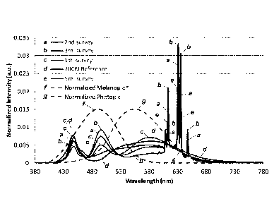
compare spectral outputs of the High PB light sources to the 70 CRI PoR light
source. The first row of the table identifies, in the first through ninth
columns,
25 the following: the survey, the booth setup (e.g., unfilled versus
filled), the
spectra source, luminous flux (Im/W) and percentage change versus the PoR
source, perceived brightness increase predicted by the MPB model, perceived
brightness increase produced by the V(I)10 model, perceived brightness
increase (percent) observed by the test subjects, calculated perceived
brightness per watt (percent) relative to the 70 CRI PoR source, and
Melanopic/Photopic (M/P) ratio calculated for emissions of the spectra source.
The second row of the table corresponds to the 70 CRI PoR source,
embodying a Creee EasyWhite (EZW) emitter (Cree, Inc., Durham, NC)
CA 03099124 2020-11-02
WO 2019/217238
PCT/US2019/030626
26
including at least one blue LED configured to stimulate emissions from a YAG
phosphor and a short nitride red phosphor. The third through seventh rows of
the table correspond to the first, second, fourth, third, and fifth booth
surveys,
respectively. The light sources for the foregoing booth surveys have been
described previously herein. The light source for the fourth booth survey is
the same as for the second survey, but the fourth booth survey utilized a low
lux test (down to 1001x) to determine whether the perceived brightness
increase would be maintained at different lux levels. As shown in the seventh
column ("experimental results"), the perceived brightness gain is
substantially
maintained over a wide range of illuminance (e.g., 900Ix in the second booth
survey, and as low as 100Ix in the fourth booth survey).
[00108] With continued reference to FIG. 6A, the sixth row provides results
for the third booth survey. The light source for the third booth survey
exhibited
the greatest increase in perceived brightness (e.g., 21%, as shown in the
seventh column), but also the lowest color rendering (i.e., a CRI value of 45,
representing a level generally below a minimum standard for general
illumination). This shows that increasing the cyan spectral content above a
certain extent may have a detrimental impact on color quality, despite the
beneficial increase in perceived brightness.
.. [00109] The seventh row of the table of FIG. 6A provides results for the
fifth
booth survey. The light source for the fifth booth survey exhibited the only
increase of all sources in perceived brightness per watt relative to the PoR
light source ¨ notably, while also significantly enhancing color rendering,
increasing to a CRI value of 90 relative to the CRI value of 70 for the PoR
source. This is attributable in significant part to utilization of the well-
optimized GNYAG (green) phosphor in the light source for the fifth booth
survey, versus utilization of less-well-optimized cyan phosphors in the light
sources for the first through fourth booth surveys. It is believed that
further
development and optimization of cyan phosphors will enable increased
perceived brightness sources with greater perceived brightness per watt to be
provided.
[00110] FIG. 6B is a table identifying results of a sixth booth survey
utilizing
the above-described side-by-side illuminated booths to compare a 78 CRI
CA 03099124 2020-11-02
WO 2019/217238
PCT/US2019/030626
27
LED-based High PB light source (similar to the light source of the second and
fourth booth surveys) to an 80 CRI PoR LED light source including at least
one blue LED configured to stimulate emissions from a YAG phosphor and a
short nitride red phosphor. The table of FIG. 6B includes the same columns
as provided in the table of FIG. 6A. As shown, the High PB light source
provided emissions having a perceived brightness 7.1% greater than that of
the PoR light source with a similar color fidelity (i.e., a CRI values of 78
versus
80 for the PoR source), but exhibited a lower perceived brightness per watt.
[00111] FIG. 7A provides spectral power distribution plots (in normalized
intensity versus wavelength) for the light sources utilized in the booth
surveys
described in connection with FIG. 6A. As shown, the spectral power
distribution for the PoR source (i.e., PoR EZW 4000K 70 CRI, labeled "d') in a
cyan range is the least of all depicted light sources. Also, the light source
for
the third booth survey (labeled "b") exhibits the most prominent peaks for
cyan, amber, and red content, while exhibiting the least spectral energy
content between roughly 530-590 nm, thereby explaining the low CRI value of
45 shown in the table of FIG. 6A for this light source.
[00112] FIG. 7B provides the same image as FIG. 7A, with addition of
normalized melanopic and normalized photopic spectral power distribution
(SPD) plots. As shown, the normalized melanopic response curve plot has a
peak near 490 nm (thereby encompassing the cyan peaks for various light
sources), and the normalized photopic SPD plot has a peak near about 565
nm (thereby encompassing the amber peaks for various light sources). The
normalized melanopic and photopic response curves also overlap significantly
with one another.
[00113] A Melanopic/Photopic ratio ("M/P ratio") may be defined for a
particular light source by dividing an integrated spectral output of the light
source coincident with the melanopic response curve by an integrated
spectral output of the light source coincident with the photopic response
curve, according to the following equation:
CA 03099124 2020-11-02
WO 2019/217238
PCT/US2019/030626
28
i380 M (A) d
KIP ratio= 780
1380 14,1) / (A) d A
[00114] FIG. 8 is a plot of perceived brightness gain versus
melanopic/photopic spectral ratio (M/P ratio) for the light sources utilized
in
the first through fifth booth surveys described in connection with FIG. 6A. In
addition, data is plotted for comparison of POR 70 CRI on both sides (M/P
ratio of approximately 0.46) showing no perceived brightness gain, as
expected. As shown, perceived brightness gain appears to be directly
proportional to M/P ratio, with a polynomial curvefit value being provided for
the data points corresponding to the four light sources. As noted previously,
however, it is not trivial to enhance perceived brightness while at the same
time also maintain color rendering values at or above a minimum value (e.g.,
CRI Ra value of at least 70, 75, 80, 85, or another threshold specified
herein)
sufficient for general illumination.
[00115] FIG. 9 provides plots and superimposed curvefits of
melanopic/photopic spectral ratio versus CCT for the first PoR 70 CRI light
source, for the High PB light source used in the fifth booth survey, and for a
modeled High PB light source having at least 70 CRI ¨ with addition of data
points for a commercially available Soraa Vivid 95 CRI light source and for an
artificial skylight with a mid-day sun and sky setting for the purpose of
comparison. Each illustrated curve slopes upward to the right, indicating that
M/P ratio generally increases with CCT for the illustrated range (e.g., 2200K
to about 5400K). The lowermost curve (c) corresponds to a conventional
light source. The next curve (b) upward from the lowermost curve
corresponds to the High PB light source used in the fifth booth survey
(including a blue LED arranged to stimulate each of a green YAG (GNYAG)
phosphor with a peak wavelength of about 526 nm, a short nitride red
phosphor with a peak of about 610 nm and FWHM of about 76 nm, and a
narrowband red KSF phosphor) providing aggregated emissions with
increased perceived brightness and a CRI Ra value of 90. An offset curve (t)
(illustrated in dashed lines) embodies a percentage offset upward from the
CA 03099124 2020-11-02
WO 2019/217238
PCT/US2019/030626
29
preceding curve (b). In certain embodiments, the percentage offset may be
5%, 10%, 15%, 20%, 25%, 30%, 35%, 40%, or 50% (corresponding to offset
multiplier coefficients 1.05, 1.10, 1.15, 1.20, 1.25, 1.30, 1.35, 1.40, and
1.50)
relative to the curve (b) corresponding to the High PB light source used in
the
fifth booth survey. The uppermost curve (a) in FIG. 9 corresponds to a
modeled High PB light source having at least 70 CRI, with such light source
embodying a solid state light emitter arranged to generate emissions having a
peak wavelength in a blue range, and configured to stimulate emissions of
first through third lumiphoric materials having peak wavelengths in ranges of
from 485 nm to 530 nm, from 575 nm to 595 nm, and from 605 nm to 640 nm,
respectively, wherein the third peak wavelength corresponds to a third peak
having a full width half maximum value of less than 60 nm. Curvefit functions
for the curves shown in solid lines (curves c', b' and a') are also provided
in
FIG. 9.
[00116] An area between the curves b' and a' corresponds to blue solid
state emitter-pumped multi-phosphor light sources configured to provide high
perceived brightness in combination with suitably high color rendering values,
and that differentiate light sources known in the art (e.g., a PoR 70 CRI
light
source represented by curve c). The Soraa Vivid 95 CRI light source
corresponding to data points din FIG. 9 may provide similar M/P ratio values,
but includes phosphors pumped with a violet (405 nm peak) LED (i.e., not a
blue LED), and may exhibit lower efficiency (e.g., luminous efficacy). To
encompass a first desired area between the curves b' and a' of FIG. 9, in one
embodiment of the present disclosure, aggregated emissions of a lighting
device may have a spectral power distribution with a M/P ratio value within a
target range as a function of CCT (in Kelvin) of the aggregated emissions, the
target range including minimum values defined by a minimum value function
in which M/P ratio equals [-2.05x10⁻⁸(CCT)2 + 2.72x10⁻⁴(CCT) - 0.1506], and
the target range including maximum values defined by a maximum value
function in which M/P ratio equals [-2.57x10⁻⁸(CCT)2 + 3.70x10⁻⁴(CCT) -
0.1889]. In certain embodiments, a CCT value of the aggregated emissions
may be in a range of from 2000 to 7000K, or from 2000 to 6000K, or from
2000 to 5500K, or from 2200 to 5500K. In certain embodiments, to
CA 03099124 2020-11-02
WO 2019/217238
PCT/US2019/030626
encompass a second desired area between the curves f and a' of FIG. 9,
aggregated emissions of a lighting device may have a spectral power
distribution with a M/P ratio value within a target subrange as a function of
CCT (in Kelvin) of the aggregated emissions, the target subrange including
5 minimum values defined by a minimum value function in which M/P ratio
equals [(offset multiplier coefficient)x ([-2.05x10⁻⁸(CCT)2 + 2.72x10⁻⁴(CCT) ¨
0.1506]), the target range including maximum values defined by a maximum
value function in which M/P ratio equals [-2.57x10⁻⁸(CCT)2+ 3.70x10⁻⁴(CCT) -
0.1889]. As noted previously, the offset multiplier coefficient in certain
10 embodiments may have a value of 1.05, 1.10, 1.15, 1.20, 1.25, 1.30,
1.35,
1.40, or 1.50.
[00117] The preceding discussion of enhanced perceived brightness light
sources providing suitably high color rendering index values addressed color
points on the blackbody locus. To consider whether enhanced perceived
15 brightness in combination with suitably high color rendering index
values may
be obtained for light sources producing color points off the blackbody locus
(BBL), computer modeling was performed for light sources corresponding the
High PB light source used in the fifth booth survey (described as "EZW with
NBR 90CRI" in FIG. 10A), and for a High PB light source having at least 70
20 CRI (as mentioned in connection with FIG. 9, and described as "High PB
with
NBR 700RI" in FIG. 10A) for color points on, above (e.g., MacAdam 2-step
and 4-step ellipses above), and below (e.g., MacAdam 2-step and 4-step
ellipses below) the BBL. Results of such modeling are shown in FIGS. 10A-
100. The lower set of curves in FIG. 10A (and shown in FIG. 10B)
25 correspond to the "EZW with NBR 900RI" light source, with such terms
signifying "EasyWhite with narrowband red, 90 CRI." Such light source
included a 450 nm peak wavelength blue LED arranged to stimulate
emissions of a GNYAG green phosphor, a short nitride red phosphor, and a
narrowband red KSF phosphor. In FIG. 10B, for the whole CCT range, at the
30 same CCT, the above-BBL color points exhibited a lower M/P ratio than the
below-BBL color points, and color points farther away from the BBL exhibited
larger M/P ratio differences. The upper set of curves in FIG. 10A (and shown
in FIG. 100) correspond to the "High PB with NBR 70CRI" light source, with
CA 03099124 2020-11-02
WO 2019/217238
PCT/US2019/030626
31
such terms signifying "increased perceived brightness with narrowband red,
70 CRI." Such light source included a 450 nm peak wavelength blue LED
arranged to stimulate emissions of a cyan phosphor, an amber phosphor, and
a narrowband red KSF phosphor. In FIG. 10C, for CCT values below 4000K,
at the same CCT, the above-BBL color points exhibited lower M/P ratios than
the below-BBL color points. For CCT values above 4000K, the foregoing
trend was not maintained. As shown in FIGS. 10A-10C, desired combinations
of enhanced perceived brightness and suitably high color rendering index
values may be obtained not only for color points on the BBL, but also to color
points proximate to the BBL. Based on extrapolation of the data reflected in
FIG. 10A, the desired combination of features is believed to be attainable for
color points within a MacAdam 10 step ellipse of the BBL.
[00118] FIG. 11 shows color points for first and second light sources "E2
2A" and "E2 2B" arranged below and above the BBL, respectively, at a CCT
value of just above 6000K, in a magnified portion of a 1931 CIE chromaticity
diagram, and corresponding to modeling results discussed in connection with
FIGS. 10A-10C. Each of the first and second color points E2 2A, E2 2B is
offset from the BBL by a duv value of 0.004, corresponding to a MacAdam 4-
step ellipse.
[00119] FIG. 12 provides spectral power distribution plots (in normalized
intensity versus wavelength) for the two light sources (namely, E2 2A and E2
2B) of FIG. 11, with a superimposed normalized melanopic spectral power
function plot. FIG. 13 is a table identifying duv, CCT, CRI, and M/P ratio
values for two light sources E2 2A and E2 2B of FIGS. 11 and 12. In general,
at the same CCT, above-BBL spectral power distributions have lower M/P
ratio than below-BBL spectral power distributions for the same emitter plus
phosphor blend, since below-BBL spectral power distributions have a higher
"blue peak," and thus a higher M/P ratio. An exception to this general rule is
encountered when the "cyan peak" is very close to the "blue peak (such as in
the E2 bin shown in FIG. 11). Referring to FIG. 13, the "E2 2B" spectral
power distribution exhibited a higher M/P ratio than the "E2 2A" spectral
power distribution at the same CCT.
CA 03099124 2020-11-02
WO 2019/217238
PCT/US2019/030626
32
[00120] As noted previously, in certain embodiments, one of the spectral
peaks mentioned above may be provided by a supplemental (e.g., cyan,
green, amber/orange, or red) electrically activated solid state light emitter
(e.g., an LED) instead of a lumiphoric material. In certain embodiments, all
electrically activated solid state light emitters may be covered with a single
lens, diffuser, and/or optical element. In certain
embodiments, a
supplemental electrically activated solid state light emitter is configured to
provide narrowband red output (e.g., in a range of from 605 nm to 640 nm, or
in a subrange of from 610 nm to 635 nm, or in a subrange of from 610 nm to
.. 625 nm). In certain embodiments, a supplemental electrically activated
solid
state light emitter is configured to provide cyan or cyan/green output (e.g.,
in a
range of from 485 nm to 530 nm, or in a subrange of from 485 nm to 505 nm,
or in a subrange of from 490 nm to 500 nm). In certain embodiments, any
supplemental electrically activated solid state light emitters are controlled
in
.. tandem with (i.e., not independently from) the (e.g., blue-emitting)
electrically
activated solid state light emitter(s). In certain
embodiments, any
supplemental electrically activated solid state light emitters may be
independently controlled relative the (e.g., blue-emitting) electrically
activated
solid state light emitter(s).
[00121] Having described desirable combinations of solid state emitters and
lumiphoric materials, solid state lighting devices that may incorporate such
emitters and lumiphoric materials will now be described.
[00122] In certain embodiments, one or more solid state emitters and
lumiphoric materials may be provided in a single-chip or multi-chip LED
package.
[00123] FIG. 14 illustrates a LED package 100 a single LED chip 101
mounted on a reflective cup 102 using solder or a conductive epoxy, such that
ohmic contacts for the cathode (or anode) of the LED chip 101 are electrically
coupled to the bottom of the reflective cup 102. The reflective cup 102 is
.. either coupled to or integrally formed with a first lead 103 of the LED
package
100. One or more bond wires 104 connect ohmic contacts for the anode (or
cathode) of the LED chip 101 to a second lead 105. The reflective cup 102
may be filled with an encapsulant material 106 that encapsulates the LED
CA 03099124 2020-11-02
WO 2019/217238
PCT/US2019/030626
33
chip 101. The encapsulant material 106 may be clear or contain one or more
wavelength conversion materials, such as phosphors or other lumiphoric
materials. The entire assembly is encapsulated in a clear protective resin
107, which may be molded in the shape of a lens to control the light emitted
.. from the LED chip 101 and any lumiphoric material(s) contained in the
reflective cup 102.
[00124] An alternative LED package 110 is illustrated in FIG. 15 wherein a
LED chip 111 is mounted on a substrate 114. Ohmic contacts for the anode
(or cathode) of the LED chip 111 are directly mounted to first contact pads
.. 115 on the surface of the substrate 114. The ohmic contacts for the cathode
(or anode) of the LED chip 111 are connected to second contact pads 116,
which are also on the surface of the substrate 114, using bond wires 117.
The LED chip 111 resides in a cavity of a reflector structure 118, which is
formed from a reflective material and functions to reflect light emitted from
the
LED chip 111 through the opening formed by the reflector structure 118. The
cavity formed by the reflector structure 118 may be filled with an encapsulant
material 112 that encapsulates the LED chip 111. The encapsulant material
112 may be clear or contain at least one wavelength conversion material,
such as one or more phosphors or other lumiphoric materials.
[00125] FIGS. 16A-19B illustrate exemplary portions of solid state lighting
devices in different configurations incorporating electrically activated solid
state light emitters arranged over package mounts (or other substrates) and
optionally overlaid with lenses, wherein such devices may be used alone or in
groups according to certain embodiments described herein. It is to be
.. appreciated that various structures employed within complete lighting
devices
(e.g., package leads, leadframes, contacts, wirebonds, bond structures, heat
transfer elements, diffusers, additional reflecting surfaces, power supplies,
and the like) have been omitted for clarity of illustration, but one skilled
in the
art would appreciate that known structures could be incorporated in operative
lighting devices including the illustrative portions provided in FIGS. 16A-
19B.
[00126] FIG. 16A illustrates a solid state light emitting device 120 including
at least one solid state emitter (e.g., LED) chip 123 (which may include LED
epitaxial layers and a support) arranged over a top surface 122 of a package
CA 03099124 2020-11-02
WO 2019/217238
PCT/US2019/030626
34
mount (or other substrate) 121, with a top surface 124 of the solid state
emitter chip 123 being covered with at least one lumiphoric material 126
(e.g.,
a mixture or dispersion of different lumiphoric materials as disclosed
herein).
The package mount 121 may include metalized regions and/or vias (not
shown) for conduction of electrical signals to the solid state emitter chip
123.
Side surfaces 125 of the solid state emitter chip 123 may be exposed, or in
certain embodiments may be coated with one or more materials or
encapsulant.
[00127] FIG. 16B illustrates a solid state light emitting device 120A
including
the device 120 of FIG. 16A following addition of a lens 129 having a curved
(e.g., substantially hemispherical) shape. Such lens 129 may be formed by
any suitable method, including but not limited to molding using silicone
material. In certain embodiments, the lens 129 may have a width or lateral
extent that is substantially equal to a width or lateral extent of the package
mount 121, and a peripheral portion 129A of the lens 129 may have a
substantially uniform thickness.
[00128] FIG. 17A illustrates a solid state light emitting device 130 including
a solid state emitter (e.g., LED) chip 133 (which may include LED epitaxial
layers and a support) arranged over an upper surface 132 of a package
mount (or other substrate) 131, with a top surface 134 and side surfaces 135
of the solid state emitter chip 133, as well the upper surface 132 of the
package mount 131, being covered with wavelength conversion (e.g.,
lumiphoric) material 136. In certain embodiments, the LED chip 133 may be
mounted to the package mount 131, and thereafter the LED chip 133 and
upper surface 132 of the package mount 131 may be coated with lumiphoric
material 136. Coating may be performed according to any suitable process
disclosed herein, such as spray coating, dipping, or the like. Such materials
136, 138 may be arranged in conformal layers that follow the shape and
outline of multiple surfaces of the solid state emitter chip 133. Electrical
connections to the LED chip 133 may be made either before or after coating
steps.
[00129] FIG. 17B illustrates a solid state light emitting device 130A
including
the device 130 of FIG. 17A following addition of a lens 139 having a
CA 03099124 2020-11-02
WO 2019/217238
PCT/US2019/030626
substantially rectangular cross-sectional curved (e.g., substantially
hemispherical) shape. Such lens 139 may be formed by any suitable method,
including but not limited to molding using silicone material. In certain
embodiments, the lens 139 may have a width or lateral extent that is
5 substantially equal to a width or lateral extent of the package mount
131.
[00130] FIG. 18A illustrates a solid state light emitting device 140 including
a solid state emitter (e.g., LED) chip 143 (which may include LED epitaxial
layers and a support) arranged over a upper surface 142 of a package mount
(or other substrate) 141, with a top surface 144 of the solid state emitter
chip
10 143 being covered with first through third layers 146, 147, 148 of
lumiphoric
materials. The package mount 141 may include metalized regions and/or vias
(not shown) for conduction of electrical signals to the solid state emitter
chip
143. Side surfaces 145 of the solid state emitter chip 143 may be exposed or
otherwise coated lumiphoric material. In certain embodiments, the LED chip
15 143 may be coated with lumiphoric materials 146-148, and thereafter the
pre-
coated LED chip 143 may be mounted to the package mount 141 followed by
establishment of suitable electrically conductive connection(s) to the LED
chip
143. Coating may be performed according to any suitable process disclosed
herein, such as spray coating.
20 [00131] FIG. 18B illustrates a solid state light emitting device 140A
including
the device 140 of FIG. 18A following addition of a lens 149 having a curved
(e.g., substantially hemispherical) shape. Such lens 149 may be formed by
any suitable method, including but not limited to molding using silicone
material. In certain embodiments, the lens 149 may have a width or lateral
25 extent that is substantially equal to a width or lateral extent of the
package
mount 141, and a peripheral portion 149A of the lens 149 may have a
substantially uniform thickness.
[00132] FIG. 19A illustrates a solid state light emitting device 150 including
a solid state emitter (e.g., LED) chip 153 (which may include LED epitaxial
30 layers and a support) arranged over an upper surface 152 of a package
mount (or other substrate) 151, with a top surface 154 and side surfaces 155
of the solid state emitter chip 153, as well as an upper surface 152 of the
package mount 151, being covered with first through third layers of lumiphoric
CA 03099124 2020-11-02
WO 2019/217238
PCT/US2019/030626
36
material 156, 157, 158. In certain embodiments, the LED chip 153 may be
mounted to the package mount 151, and thereafter the LED chip 153 and
upper surface 152 of the package mount 151 may be coated with the
lumiphoric material layers 156-158. Coating may be performed according to
any suitable process disclosed herein, such as spray coating. The lumiphoric
material layers 156-158 may be arranged in conformal layers that follow the
shape and outline of multiple surfaces of the solid state emitter chip 153.
Electrical connections to the LED chip 155 may be made either before or after
coating steps.
.. [00133] FIG. 19B illustrates a solid state light emitting device 150A
including
the device 150 of FIG. 19A following addition of a lens 159 having a
substantially rectangular cross-sectional curved (e.g., substantially
hemispherical) shape. Such lens 159 may be formed by any suitable method,
including but not limited to molding using silicone material. In certain
embodiments, the lens 159 may have a width or lateral extent that is
substantially equal to a width or lateral extent of the package mount 151.
[00134] Although specific lens shapes are illustrated in FIGS. 16B, 17B,
18B, 19B, it is to be appreciated that lenses according to any suitable shapes
may be applied to any of the lighting devices illustrated in FIGS. 16A-19B.
For example, symmetric, non-symmetric, polygonal, truncated hemispherical,
faceted, textured, and/or trench-defining lenses may be used.
[00135] FIG. 20 is a side cross-sectional view of at least a portion of a
solid
state light emitting device 160 including multiple solid state emitter (e.g.,
LED)
chips 165 arranged over a submount 161 in flip-chip configuration, with both
anode and cathode connections on the bottom of the chips 165. The solid
state emitter chips 165 may (optionally) include angled or beveled upper
edges with a non-rectangular (e.g., polygonal) cross-section, with such shape
serving to enhance light extraction. The solid state emitter chips 165 are
coated or otherwise covered with one or more lumiphoric materials 166 (e.g.,
in one or more conformal layers) and arranged under a hemispherical optical
element (e.g., lens) 169, with the conformal layer(s) 166 following the shape
and contour of multiple surfaces of the solid state emitter chips 165
(preferably with substantially constant thickness). Such coating may be
CA 03099124 2020-11-02
WO 2019/217238
PCT/US2019/030626
37
performed using any coating technique disclosed herein or otherwise known
in the art. As shown in FIG. 20, the conformal layer(s) 166 may extend over,
between and laterally beyond the solid state emitter chips 165 (such as over a
reflective material disposed between or adjacent to the solid state emitter
chips 165). The optical element 169 may be separated from the solid state
emitter chips 165 via a gap or an intervening material 168, which may include
encapsulant or a fluid medium such as liquid or gel (e.g., mineral oil,
perfluorinated polyether (PFPE) liquid, or other fluorinated or halogenated
liquid or gel). Such intervening material 168 may also include an index
matching medium characterized by a refractive index that provides for
reduced or minimal reflection or internal refraction of light emissions. In
certain embodiments, elements 168, 169 may embody a single element, such
as molded silicone. In certain embodiments, a thickness of each conformal
layer 166 may be less than half the spacing between adjacent solid state
emitter chips 165. In certain embodiments, spacing between solid state
emitter chips 165 may be on the order of 10 to 75 micrometers, although
larger spacing (up to 150 or even 500 micrometers) may also be used. In
certain embodiments, the optical element 169 may include one or more
functional materials, such as lumiphoric material, filtering material, and/or
scattering material, which may be doped, coated, or otherwise provided in or
on the optical element 169. Still referring to FIG. 20, the submount 161
(e.g.,
alumina, aluminum nitride, high temperature polymers, etc.) is covered with a
pattern of metal (e.g., traces) 163 that may be used to interconnect the solid
state emitter chips 165 and provide connection to a power supply (not shown).
The metal pattern 163 includes connection pads 162 with insulating material
164 therebetween.
[00136] FIG. 21 illustrates a solid state emitter package 180 including
multiple solid state emitter (e.g., LED) chips 185 coupled to electrical
traces or
metal patterns 182 via wirebonds 186 and arranged under a hemispherical
optical element (e.g., lens) 189. In certain embodiments, one or more LED
chips 185 is coated with one or more lumiphoric material. As shown, twelve
solid state emitter chips 185 are provided in contact with the electrical
traces
or metal patterns 182 arranged over submount 181, and cathodes of the LED
CA 03099124 2020-11-02
WO 2019/217238
PCT/US2019/030626
38
chips are connected by wirebonds 186 to electrical traces or metal patterns
182. In certain embodiments, the optical element 189 may include one or
more functional materials, such as lumiphoric material, notch filtering
material,
and/or scattering material, which may be doped, coated, or otherwise
provided in or on the optical element 189. The solid state emitter chips 185
may be selected from various light color bins to provide a combined light
output with appropriate color characteristics for a desired application. The
unfiltered efficiency of such a solid state emitter package 180 with a warm
white color may be on the order of 100 lm/W, prior to any filtering from the
optical element; however, if the solid state emitter package 180 is binned for
a
cool white color, then an efficiency on the order of about 150 Im/VV can be
achieved (i.e., prior to any filtering).
[00137] FIGS. 22A-22D illustrate a lighting device according to one
embodiment of the disclosure, embodied in a substantially cylindrical
downlight 200 intended for in-ceiling mounting and including multiple LEDs as
part of a LED module 206. The downlight 200 includes a generally cylindrical
base housing 201 and a heatsink housing 205 that in combination form a
body structure. Mounting elements 214 such as rotatable spring tabs are
arranged along an upper surface 215 of the housing 201. A cable 218
extends between the base housing 201 and an Edison (screw-type) male
connector forming a threaded lateral contact 212 and a foot contact 211. The
base housing 201 defines an interior volume 202 containing printed circuit
boards 203, 204 that include operative elements such a power converter, a
controller module (e.g., including at least one processor and a memory), one
or more transceivers (e.g., wireless transceivers), LED driver modules, sensor
modules, detectors, voice recognition circuitry, and the like. The heatsink
housing 205 defines an inner cavity 209 that includes a reflective surface and
is further bounded by a light transmissive optical element such as a lens
and/or a diffuser. A trim bezel 213 is arranged proximate to an open end of
the heatsink housing. The downlight 200 may include any suitable features
disclosed herein, and is preferably arranged to execute any one or more
functions and/or method steps described herein.
CA 03099124 2020-11-02
WO 2019/217238
PCT/US2019/030626
39
[00138] FIGS. 23A-23B illustrate a light bulb 240 including multiple LEDs
247 arranged in a two-dimensional array within a cavity bounded by a light
transmissive globe or lens 250 according to one embodiment of the
disclosure. Each LED 247 may have associated therewith multiple lumiphoric
materials. The LEDs 247 are arranged on a single substantially planar emitter
support surface 246, which may be elevated by a pedestal 254. The light bulb
240 includes a body structure 241 having an associated external heatsink
245. An Edison (screw-type) connector including a threaded lateral contact
252 and a foot contact 251 extend from one end of the body structure 241
opposing the globe 250. The body structure 241 defines an interior volume
containing at least one printed circuit board (not shown) that includes
operative elements such as a power converter, a controller module (e.g.,
including at least one processor and a memory), one or more transceivers
(e.g., wireless transceivers), LED driver modules, sensor modules, detectors,
voice recognition circuitry, and the like. The light bulb 240 may include any
suitable features disclosed herein.
[00139] FIGS. 24A-24B illustrate a troffer-type (in-ceiling linear) light
fixture
300 arranged to incorporate multiple solid state emitters (e.g., LEDs) 326 as
disclosed herein. In certain embodiments, one or more lumiphoric materials
may be associated with one or more LEDs 326. Optionally, the light fixture
300 may include one or more notch filtering materials, such as may be
associated with solid state emitters 326, may be applied to or included in a
linear reflector (e.g., e.g., by doping, impregnation, coating, etc.), or may
be
applied to or integrated with one or more light transmissive lens plates 315,
316 to cause the light emitted from the light fixture 300 to exhibit a
spectral
notch. Light fixture 300 includes pan 301, heatsink 302, reflector 308, and
end
caps 310, 311. End cap 310 is larger than end cap 311 and is shaped to act
as a circuit box to house electronics used to drive and control the light
source
(e.g., rectifiers, regulators, timing circuitry, etc.). The reflector 308 may
include
a diffusively reflective or specularly reflective surface 318. Although a
reflector may take various shapes, in the illustrated embodiment, the
reflector
308 includes a flat region 324 opposite the heatsink 302. In alternative
embodiments, the reflector 308 could be parabolic in shape, or include two or
CA 03099124 2020-11-02
WO 2019/217238
PCT/US2019/030626
more parabolic regions. Light fixture 300 also includes a diffuser lens
assembly including lens plates 315, 316, disposed adjacent to sides of the
heatsink 302.
[00140] FIGS. 25A and 25B illustrate a high bay/low bay type solid state
5 lighting fixture 330 including a frame 332 over which a heatsink 334 and
an
electronics housing 336 are mounted. An LED array 338 is mounted on a
bottom side of the frame 332 and may be covered by a lens 340. As
illustrated, a portion of the lens 340 is shown as being removed to expose the
LED array 338. A reflector 342 may be provided around the LED array 338 to
10 aid in directing and mixing light emitted from the LED array 338 for
general
illumination.
[00141] FIGS. 26A-26B illustrate a first outdoor floodlight (e.g., street or
roadway lamp) 400 that may include multiple solid state light emitters as
described herein. The floodlight 400 includes a housing 410 including a base
15 portion 411 supported by an elongated pole 401 or other support.
Multiple
LEDs modules 431-1, 431-2, 431-3 each including multiple LEDs 418A, 418B
arranged in an array are provided along a lower surface 420 of the floodlight
400 between the pole 401 and an end cap 412. The LED modules 431-1, 431-
2, 431-3 are arranged proximate to an air gap 414 permitting heat to be
20 dissipated to a heat spreader or heat sink 426 (arranged along an upper
surface 413 of the housing 410) and transferred to an ambient environment.
The floodlight 400 may include at least one receiver or sensor element 440-1,
440-2, which may embody any one or more of GPS receiver, a radio
frequency receiver, an ambient light sensor, an image sensor, a temperature
25 sensor, a motion sensor, a sound sensor, a timer, or the like.
[00142] FIGS. 27A-27B illustrate a second outdoor floodlight fixture 450
including a body structure 402 housing an array of solid state light emitters
404 as disclosed herein. An interface structure 406 may be used to couple
the floodlight fixture 450 to a pole 410. Outdoor light fixtures such as shown
30 in FIGS. 27A-27B may be mounted to poles, tenons, or the like. The array
of
solid state light emitters 404 may be used to illuminate a desired
environment,
such as a roadway, a parking lot, a street, or the like.
CA 03099124 2020-11-02
WO 2019/217238
PCT/US2019/030626
41
[00143] Embodiments as disclosed herein may provide one or more of the
following beneficial technical effects: enhancing perceived brightness of
illumination provided by lighting devices while maintaining desirable color
rendering characteristics; and reducing energy consumption required for light
fixtures to provide equivalent perceived brightness levels.
[00144] Those skilled in the art will recognize improvements and
modifications to the preferred embodiments of the present disclosure. All
such improvements and modifications are considered within the scope of the
concepts disclosed herein and the claims that follow.