Note: Descriptions are shown in the official language in which they were submitted.
CA 03100064 2020-11-12
WO 2019/226264
PCT/US2019/028711
LINK 16 TRANSCEIVER WITH INTEGRAL SIGNAL NULLING SYSTEM
FIELD
[0001] The following disclosure relates generally to secure wireless network
communications, and more particularly to methods for mitigating jamming
attacks in
tactical wireless communication networks.
BACKGROUND
[0002] One of the requirements for virtually any communication system is the
ability to operate reliably over an entire geographical region of interest,
despite the
presence of various sources of noise, naturally occurring interference, and
signal
obstructions. In the case of military communication systems, and also for some
civilian communication systems, the challenge of providing reliable
communications
can be greatly increased due to adverse circumstances, such as when operating
in
Anti-Access Area Denial (A2AD) regions where communications are contested due
to the presence of adversarial signals such as adversarial communications,
navigation, and jamming signals. In particular, because wireless communication
networks are critically important for maintaining coordination and
intercommunication between elements of mobile combat assets, it is vital that
secure, tactical networks remain resilient in the presence of jamming threats.
[0003] When operating in A2AD regions, it is also typically necessary that at
least
some communications be rendered difficult or impossible for adversaries to
intercept
and/or interpret. Current approaches that are used to meet these COMSEC
(communications security) requirements include various forms of cryptography,
referred to as message security or MSEC, as well as transmission security,
referred
to as TSEC or TRANSEC. TRANSEC typically includes pseudorandom frequency
hopping and/or signal covers, wherein a required pseudorandom sequence
generation
is controlled by a cryptographic algorithm and key. Examples of these
approaches
include Link 16, Tactical Targeting Networking Technology (TTNT) and Common
Data Link (CDL). In particular, Link 16 is a widespread tactical wireless
networking system that is used by frontline land, air, and naval systems in
the
1
CA 03100064 2020-11-12
WO 2019/226264
PCT/US2019/028711
United States, NATO, and allied nations to allow multiple users to share
situational
awareness data.
[0004] In a Link 16 network, information can be transmitted simultaneously on
any or all of 51 frequencies that span a designated Link 16 bandwidth
(typically 960
MHz to 1,215 MHz) during each of a plurality of timeslots that repeat every
time
frame, or "epoch." Messages in a Link 16 network are typically transmitted
over
logical "channels," where each channel is defined and characterized by a
unique
assignment of timeslots and frequency hopping patterns. Often, a Link 16
transceiver is able to simultaneously monitor more than one of these logical
channels. For example, a "CMN-4" transceiver is able to perform "concurrent
multi-
netting" communication on four channels.
[0005] A typical link 16 network is illustrated in Fig. 1. The blocks 10 in
the
epoch ring 12 represent timeslots, and the stacked rings in the column 16
represent
the logical "channels" of the Link 16 network. Accordingly, a plurality of
participants 14 are able to communicate simultaneously over the link 16
network
because they are assigned to different channels 16 during each timeslot 10
and/or to
different timeslots 10 during each epoch 12. The Link 16 messages transmitted
within the network include Precise Participant Location and Identification
(PPLI)
messages that are exchanged between the nodes. Details of the construction of
the
PPLI messages can be found in MIL-STD-6016.
[0006] Despite its inherent anti-jamming features, the effective communication
range of a Link-16 network can nevertheless be significantly reduced by an
interfering adversary transmitting a focused, localized, high power jamming
signal
toward the Link-16 nodes. Sometimes, the effects of jamming in a Link 16
network
can be mitigated to some extent by increasing transmission powers of the Link
16
nodes and/or by relaying signals through intermediate nodes so as to reduce
transmission distances. However, this approach can be expensive, and can
suffer
from terrain obstructions and shadowing, and from radio horizon limitations.
Furthermore, appropriate relay nodes may not be available, or it may not be
desirable to burden nodes with the overhead of relaying messages. As a result,
unwanted or "enemy" transmissions that are detected by a Link 16 receiver,
2
CA 03100064 2020-11-12
WO 2019/226264
PCT/US2019/028711
especially hostile jamming signals, are often much stronger than the signals
that are
received from desired or "friendly" sources.
[0007] Other than increasing power and/or relaying messages, an additional
approach that can be used to mitigate jamming attacks is to apply signal
nulling to
the received signals. According to this approach, and with reference to Fig.
2A, a
separate nulling apparatus 200 samples the entire Link 16 bandwidth using an
array
antenna 202, applies signal nulling to the received signals, and then
transmits the
nulled signal data to the Link 16 transceiver, where the applicable TRANSEC
and
COMSEC keys are used to channelize, extract, and decode the link 16 messages
included in the received signals.
[0008] With reference to Fig. 2B, according to this approach the nulling
apparatus
200 converts all of the energy received within the Link 16 bandwidth by each
of the
array antennae 202 into digital data 206, after which an internal processor
208 uses a
nulling algorithm to calculate 208 and apply separate weighting factors 210 to
the
signals from each of the antennae 202 in the array. In various embodiments,
the
nulling algorithm can be similar to nulling algorithms known in the art that
are
implemented as filters used for removing interferences from received GPS
signals,
such as the "Space Time Adaptive Processing"(STAP) algorithm, as taught for
example in US patent application 2008/0025446, in A. J. O'Brien, I. J. Gupta,
"An
Optimal Adaptive Filtering Algorithm with Zero Antenna-Induced Bias for GNSS
Antenna Arrays," Navigation, 57(2), Summer 2010, pp. 87-100, or as taught in
US
patent application 2015/022685.
[0009] The weighted signals are then combined 212, after which the weighting
factors are adjusted and re-applied iteratively according to the nulling
algorithm so
as to minimize the combined result.
[0010] The weighting factors as calculated in accord with the nulling
algorithm
have the effect of nullifying signals received from specific geographical
directions
or regions. However, the nulling process is typically applied "blindly," i.e.
on a
purely mathematical, heuristic basis and without any knowledge of the location
and/or orientation of the receiving antenna array, and without any knowledge
as to
the actual locations of friendly and/or hostile transmitters.
3
CA 03100064 2020-11-12
WO 2019/226264
PCT/US2019/028711
[0011] The success of this approach depends on a fundamental assumption that
the
hostile enemy (jamming) signals will always be stronger than the friendly
signals.
As a result, this approach can result in the inadvertent suppression of
friendly
signals if the friendly signals are strong. For example, if friendly nodes are
approaching a hostile location in close formation, Link 16 messages
transmitted
between the nodes may initially be stronger than a hostile jamming signal,
until the
enemy location is reached and the friendly forces spread apart.
[0012] Furthermore, nulling algorithms can suppress signals that originate in
geographic "side lobes" in addition to signals originating from the primary
nulling
lobe. These side lobe effects can interfere with transmission from friendly
forces
even when no enemy lies in that direction. The problem of side lobes is
exacerbated
by the complexity of the nulling solution that is required so as to
simultaneously null
the signals received in all 51 channels within the Link 16 bandwidth.
[0013] With reference again to Fig. 2B, an additional drawback that is
associated
with this nulling approach is that after the nulling has been performed, it is
often
necessary for the nulling apparatus to re-convert the nulled data back into an
analog
signal 214 and then re-transmit 216 the analog signal to a CMN-4 or other Link
16
transceiver 204, so that it can be received, re-digitized, and interpreted by
the
COMSEC aware transceiver 204. This additional conversion from digital format
back into analog format, and then back into digital format by the transceiver
204 can
degrade the quality of the data that is interpreted by the Link 16 transceiver
204.
[0014] Yet another disadvantage of existing approaches to Link 16 signal
nulling
are the cost, space, and weight requirements of providing an additional,
large,
expensive apparatus in addition to the Link 16 transceiver. In particular, the
required space and weight may be a significant barrier to upgrading existing
Link 16
installations to include signal nulling.
[0015] What is needed, therefore, is an apparatus and method for mitigating
the
effects of jamming on a TRANSEC-aware wireless communication transceiver such
as a Link 16 transceiver, while improving signal quality and minimizing the
risk of
inadvertent nulling of friendly signals.
4
CA 03100064 2020-11-12
WO 2019/226264
PCT/US2019/028711
SUMMARY
[0016] A TRANSEC-aware wireless communication transceiver such as a link 16
transceiver with integral nulling antenna system is disclosed that is able to
mitigate
the effects of jamming while improving signal quality and minimizing the risk
of
inadvertent nulling of friendly signals. The disclosed transceiver system
detects
signals received within the active communication bandwidth using an antenna
array.
A "System on a Chip" ("SoC") is associated with each antenna in the array, and
is
used to digitize the received data, and then to transmit the data to a
channelizer that
channelizes the data and transfers the channelized data to a nulling system.
The
nulling system applies signal nulling to the channelized data, in embodiments
only
to selected channels thereof, after which the nulled data is passed to a
message
controller for further analysis and interpretation. In embodiments, each of
the SoC's
is TRANSEC-aware, and is able to channelize the data received by its
associated
antenna element, so that the SoC's in aggregate function as the channelizer.
[0017] It should be noted that much of the present disclosure is presented
with
reference to Link 16 communication and Link 16 transceivers. However, it will
be
clear to one of skill in the art that the present disclosure is applicable to
any secure
communication system that is protected by a TRANSEC protocol, and that
requires
channelizing of received data before it can be analyzed and interpreted.
Accordingly, except where the context requires otherwise, references herein to
Link
16 should be interpreted to refer generically to all such TRANSEC-protected
communication protocols and transceivers.
[0018] In embodiments, the disclosed antenna array with SoC's is conformal,
and/or configured to be compatible as a direct replacement for an existing
Link 16
blade antenna. In some embodiments, the Link 16 transceiver is a conventional
Link
16 transceiver, such as a CMN-4 transceiver that has been modified so that the
digitizing and channelizing functions have been moved to the SoC's in the
antenna
array, and the conventional digitizing and channelizing hardware within the
transceiver has been replaced by a nulling system that is configured to apply
a
nulling algorithm to the channelized data. In some of these embodiments, the
channelized data is transferred by the SoC's to the transceiver over a
conventional
Link 16 serial data link that is overclocked so as to accommodate the
additional data
CA 03100064 2020-11-12
WO 2019/226264
PCT/US2019/028711
load. Accordingly, in embodiments of the present disclosure, signal nulling
capability can be added to a conventional Link 16 transceiver system simply by
replacing the blade antenna with the disclosed antenna array with SoC's, and
exchanging appropriate hardware in the transceiver.
[0019] Unlike previous approaches, the present nulling apparatus and method
are
"TRANSEC-aware," i.e. have access to the applicable algorithms and keys that
determine frequency hopping and timeslot assignments, and thereby define the
logical channels of the Link 16 network. Accordingly, the present nulling
apparatus
is able to apply nulling algorithms to the received data after it has been
channelized,
and embodiments are able to apply nulling selectively to only the energy
received
within the channels that are of interest, rather than to all of the energy
received
within the entire Link 16 bandwidth.
[0020] For example, a modified CMN-4 transceiver may only be able to monitor
four channels at any given time. Accordingly, in embodiments, the modified CMN-
4
system is able to apply nulling selectively to only the energy that is
received in the
signal channels that are being monitored. This approach significantly reduces
the
constraints that are placed on the nulling algorithm, effectively focusing the
nulling
process onto only the channel(s) that carry the signal of interest, and
thereby
reducing the complexity of the nulling solution, improving the nulling result,
and
reducing the occurrence of nulling "side lobes" and of unintended nulling of
friendly
signals.
[0021] Furthermore, embodiments of the present disclosure are able to apply a
Link-16 "detector" to the received data, so as to distinguish desired signals
from
jamming and other undesirable signals on the basis of signal characteristics,
rather
than signal amplitude. This approach allows embodiments of the present
disclosure
to null undesired signals and to retain desired signals, even in cases where
the
desired, friendly signals are stronger than the hostile, undesired signals. In
various
embodiments, the Link-16 signal detector discriminates on the basis of signal
features such as modulation type, pulse rise and/or fall times, pulse widths,
and/or
other characteristics of Link 16 signals that are very different from typical
jamming
signals.
6
CA 03100064 2020-11-12
WO 2019/226264
PCT/US2019/028711
[0022] Furthermore, embodiments use PPLI and other situational awareness
information provided by received Link 16 messages, in combination with
instantaneous awareness of the location and orientation of the Link 16 antenna
array,
to determine geographical directions from which friendly signals can be
expected
and/or directions from which only enemy signals can be expected, and use this
information as a basis from which to calculate initial sets of weighting
factors for
signal nulling.
[0023] And because the received data is channelized by the transceiver system
of
the present disclosure before the nulling is applied, there is no need to
reconvert the
nulled data back into analog format and then reconvert to digital format, as
is the
case with existing approaches to Link 16 nulling.
[0024] A first general aspect of the present disclosure is a Link 16
transceiver
with integral signal nulling system. The transceiver includes an antenna array
comprising a plurality of receiving antenna elements configured to receive
wireless
signals within a Link 16 bandwidth, for each of the receiving antenna
elements, a
system-on-a chip (SoC) associated with the receiving antenna element and
configured to digitize the wireless signals received by the receiving antenna,
a
TRANSEC-aware channelizer configured to channelize the digitized wireless
signals, a nulling system in data communication with the channelizer, and
configured to receive the channelized data and apply weighting factors thereto
according to a nulling algorithm so as to convert the channelized data into
nulled
data in which hostile signals included in the channelized data are suppressed
while
Link 16 messages included in the channelized data are maintained, and an MSEC-
aware Link 16 message controller in data communication with the nulling
system,
the message controller being configured to receive the nulled data and
interpret the
Link 16 messages included in the nulled data.
[0025] In embodiments, the TRANSEC-aware channelizer is included in the
SoC's, in that each SoC is TRANSEC-aware, and each SoC converts the wireless
signals received by its associated antenna element into channelized data.
7
CA 03100064 2020-11-12
WO 2019/226264
PCT/US2019/028711
[0026] In any of the preceding embodiments, the SoC's cam be configured to
channelize and transmit to the nulling system only energy received in Link 16
channels that are designated by the message controller to be channels of
interest.
[0027] Any of the preceding embodiments can further comprise a serial data
link
configured for transmission thereby of the channelized data from the SoC's to
the
nulling system. In some of these embodiments the serial data link is
configured for
overclocked communication of the channelized data. And in any of these
embodiments, the serial data link can be overclocked by a factor of between
200%
and 300%.
[0028] Any of the preceding embodiments can further comprising a Link 16
detector included in the nulling system and configured to discriminate between
Link
16 signals included in the channelized data and signals included in the
channelized
data that are not Link 16 signals, the nulling system being configured to
suppress the
data that are not Link 16 data and to maintain the Link 16 signals. In some of
these
embodiments, the Link 16 detector discriminates between link 16 signals and
data
that are not Link 16 signals on the basis of at least one of modulation type,
pulse rise
times, pulse fall times, and pulse widths.
[0029] In any of the preceding embodiments, the antenna array can be a
conformal
antenna array.
[0030] In any of the preceding embodiments, the antenna array can further
comprise a transmission blade configured for transmitting wireless signals
within the
Link 16 bandwidth.
[0031] In any of the preceding embodiments, the antenna array can be
compatible
as a direct replacement for a non-arrayed Link 16 blade antenna.
[0032] In any of the preceding embodiments, the nulling system can be able to
use
position and orientation information regarding the antenna array in
combination with
situational information that includes estimated locations of friendly
transmitters to
predict and optimize the weighting factors that are applied to the channelized
data.
8
CA 03100064 2020-11-12
WO 2019/226264
PCT/US2019/028711
[0033] In any of the preceding embodiments, the nulling system can apply a
space
time adaptive processing algorithm when calculating the weighting factors.
[0034] A second general aspect of the present disclosure is a method of
suppressing hostile wireless signals while retaining Link 16 messages. The
method
includes
a. receiving of wireless signals within a Link 16 bandwidth by a plurality
of receiving antenna elements included in an antenna array;
b. for each of the receiving antenna elements, converting of the received
wireless signals into channelized data;
c. transferring of the channelized data to a nulling system; and
d. determining a set of weighting factors according to a nulling algorithm
and applying the weighting factors to the channelized signals, thereby
converting the channelized data into nulled data in which hostile
signals included in the channelized data are suppressed while Link 16
messages included in the channelized data are maintained.
[0035] In embodiments, for each of the receiving antenna elements, the
wireless
signals received by the receiving antenna element are converted into
channelized
data by a TRANSEC-aware SoC that is associated with the receiving antenna
element.16. The method of claim 14, further comprising interpreting by an MSEC-
aware Link 16 message controller of a Link 16 message included in the nulled
data.
[0036] Any of the preceding embodiments can include only channelized data in
channels that are designated to be channels of interest are transferred by the
SoC's
to the nulling system.
[0037] In any of the preceding embodiments, the channelized data can be
transferred to the nulling system via a serial data link.
[0038] In any of the preceding embodiments, transferring the channelized data
via
the serial data link can include overclocking the serial data link. In some of
these
embodiment, overclocking the serial data link includes overclocking the serial
data
link by a factor of between 200% and 300%.
9
CA 03100064 2020-11-12
WO 2019/226264
PCT/US2019/028711
[0039] In any of the preceding embodiments, determining the weighting factors
can include using a Link 16 detector to discriminate between Link 16 signals
included in the channelized data and signals included in the channelized data
that are
not Link 16 signals. In some of these embodiments, the Link 16 detector can
discriminate between link 16 signals and data that are not Link 16 signals on
the
basis of at least one of modulation type, pulse rise times, pulse fall times,
and pulse
widths.
[0040] In any of the preceding embodiments, determining a set of weighting
factors according to a nulling algorithm can includes applying a space time
adaptive
processing algorithm.
[0041] In any of the preceding embodiments, determining the weighting factors
can include using position and orientation information regarding the antenna
array in
combination with situational information that includes estimated locations of
friendly transmitters to predict and optimize the weighting factors.
[0042] A third general aspect of the present disclosure is a method of adding
signal nulling capability to a Link 16 transceiver. The method includes
replacing an
antenna of the Link 16 transceiver with an antenna array comprising a
plurality of
receiving antenna elements configured to receive wireless signals within a
Link 16
bandwidth where, for each of the receiving antenna elements, a TRANSEC-aware
system-on-a chip (SoC) is associated with the receiving antenna element and
configured to convert the wireless signals received by the receiving antenna
element
into channelized data, removing from the Link 16 transceiver a subsystem
configured for channelizing received data, and installing within the Link 16
transceiver a nulling system in data communication with the SoC's and
configured to
receive the channelized data therefrom and apply weighting factors thereto
according
to a nulling algorithm so as to convert the channelized data into nulled data
in which
hostile signals included in the channelized data are suppressed while Link 16
messages included in the channelized data are maintained, the nulling system
being
further configured to transfer the nulled data to the Link 16 transceiver.
[0043] In embodiments, the antenna array is a conformal antenna array.
CA 03100064 2020-11-12
WO 2019/226264
PCT/US2019/028711
[0044] Any of these embodiments can further comprise reconfiguring a serial
data
link of the Link 16 transceiver so as to transfer the channelized data from
the SoC's
to the nulling system in an overclocked transfer mode. In some of these
embodiments, the overclocked transfer mode is overclocked by a factor of
between
200% and 300%.
[0045] The features and advantages described herein are not all-inclusive and,
in
particular, many additional features and advantages will be apparent to one of
ordinary skill in the art in view of the drawings, specification, and claims.
Moreover, it should be noted that the language used in the specification has
been
principally selected for readability and instructional purposes, and not to
limit the
scope of the inventive subject matter.
BRIEF DESCRIPTION OF THE DRAWINGS
[0046] Fig. 1 is a graphical illustration of a typical Link 16 channel
architecture
of the prior art;
[0047] Fig. 2A is a simplified, block diagram illustrating the relationship
between
an external nulling apparatus and a Link 16 transceiver according to the prior
art;
[0048] Fig. 2B is a detailed block diagram illustrating components of the
external
nulling apparatus of Fig. 2A;
[0049] Fig. 3A is a simplified illustration of the physical architecture of
an
embodiment of the present disclosure;
[0050] Fig. 3B is a flow diagram illustrating an embodiment of the method
of
upgrading an existing Link 16 transceiver system to include nulling capability
according to an embodiment of the present disclosure;
[0051] Fig. 4A is a simplified diagram illustrating channelizing of
received Link
16 data by an SoC according to an embodiment of the present disclosure;
[0052] Fig. 4B illustrates channelizing of received data by a plurality of
SoC's
associated with corresponding receiving antenna elements in an antenna array,
and
11
CA 03100064 2020-11-12
WO 2019/226264
PCT/US2019/028711
transmission of the channelized data to a nulling apparatus in a Link 16
transceiver
according to an embodiment of the present disclosure;
[0053] Fig. 5 is a detailed block diagram illustrating components of a
nulling
transceiver system according to an embodiment of the present disclosure; and
[0054] Fig. 6 is a flow diagram illustrating an embodiment of the method of
the
present disclosure.
DETAILED DESCRIPTION
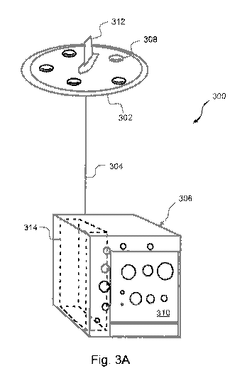
[0055] With reference to Fig. 3A, the present disclosure is a Link 16
transceiver
system 300 with integral signal nulling system 302, 304, 306 that is able to
mitigating the effects of jamming while improving signal quality and
minimizing the
risk of inadvertently nulling friendly signals. The disclosed transceiver
system 300
detects signals received within the Link 16 bandwidth using an antenna array
302. A
"System on a Chip" ("SoC") is associated with each receive antenna element 308
in
the array, and is used to digitize the received data, and then to transmit the
digitized
data to a to a TRANSEC-aware channelizer that channelizes the data and
transfers
the channelized data to a nulling system 314. The nulling system 314 applies
signal
nulling to the channelized data, in embodiments only to selected channels
thereof,
after which the nulled data is passed to a message controller 310 for further
analysis
and interpretation.
[0056] In the embodiment of Fig. 3A, each of the SoC's is TRANSEC-aware, and
is able to channelize the data received by its associated antenna element 308,
so that
the SoC's in aggregate function as the channelizer. Accordingly, the
channelized
data is transferred directly from the SoC's to the nulling system 314, which
in Fig.
3A is included with the message controller 310 in a Link 16 transceiver
unit306.
Embodiments further include a blade transmitting antenna 312 in the antenna
array
302.
[0057] In embodiments, the array antenna 302 with SoC's is conformal, and/or
configured to be compatible as a direct replacement for an existing Link 16
blade
antenna. In some embodiments, the Link 16 transceiver 306 is an otherwise
conventional Link 16 transceiver, such as a CMN-4 transceiver that has been
12
CA 03100064 2020-11-12
WO 2019/226264
PCT/US2019/028711
modified by replacing the digitizing and channelizing hardware with a nulling
system 314 that is configured to apply a nulling algorithm to the received and
channelized data. In some of these embodiments, the channelized data is
transferred
by the SoC's to the transceiver 306 over an existing serial data link 304 that
is
overclocked so as to accommodate the increased data load. Note that
overclocking
refers to operating the processor(s) of the serial data link at a higher speed
than rated
by increasing the clock speed. In one example the overclocking is done at 250%
greater than the rated speed. In a further example the overclocking is between
200%
to 300% greater than the clock speed.
[0058] Accordingly, with reference to Fig. 3B, in embodiments a conventional
Link 16 transceiver system 306 can be configured for signal nulling simply by
replacing 316 the blade antenna with the disclosed antenna array 302 with
integral
SoC's 308, removing 318 the channelizing hardware from the transceiver 306 and
replacing it 320 with a nulling system 314, and overclocking 322 the serial
data
interface 304 that transfers the channelized data from the SoC's to the
nulling
system 314.
[0059] Unlike previous approaches to nulling Link 16 signals, the present
nulling
apparatus and method are TRANSEC-aware, and are thereby able to channelize the
received data before nulling. Embodiments are further able to apply nulling
algorithms selectively to only the energy received in the channels that are of
interest,
rather than nulling all of the energy received in entire Link 16 bandwidth.
For
example, a modified CMN-4 transceiver 306 may only be able to monitor four
channels at any given time, so that it is only necessary to null the data
received in
those four channels.
[0060] Accordingly, with reference to Fig. 4A, in embodiments the received
data
400 may include four channels of interest, for example, which are indicated as
A, B,
C, and D in the figure. The data belonging to these four channels will be
distributed
among the 51 available frequencies 12 (only 8 are shown in the figure) and
among
the timeslots 10 of each epoch (only 16 timeslots are illustrated in the
figure). The
frequency hopping patterns and timeslot assignments are determined by
pseudorandom algorithms that are controlled by one or more unique keys.
However,
because the SoC chips 402 are TRANSEC-aware, they are aware of the frequency
13
CA 03100064 2020-11-12
WO 2019/226264
PCT/US2019/028711
hopping patterns and timeslot assignments that are in use, and are able to
select the
appropriate timeslots and frequencies and to assemble the received data into
channelized data 404.
[0061] With reference to Fig. 4B, each of the SoC's 402 associated with the
receive antennas 308 in the antenna array 302 receives and channelizes a full
set of
data, at least for the channels of interest, and then the channelized data
from all of
the SoC's 402 is transferred to the nulling system 314 for application of
weighting
factors according to the nulling algorithm. In embodiments, the channelized
data is
transmitted as multiplexed serial data over an existing data link 304, such as
a
conventional Link 16 RF coaxial cable. So as to accommodate all of the
required
data, in some of these embodiments the serial data link 304 is overclocked. In
embodiments, the serial data link 304 is overclocked by a factor of between
200%
and 300%.
[0062] As a result, with reference again to Fig. 3A, the nulling system 314 is
able
to apply nulling selectively to only the signal channels 404 that are being
monitored
by the message controller 310. This approach significantly reduces the
constraints
that are placed on the nulling algorithm, thereby focusing the nulling process
onto
only the channels of interest, simplifying the nulling solution, improving the
nulling
result, and reducing the occurrence of nulling "side lobes" and of unintended
nulling
of friendly signals.
[0063] Furthermore, with reference to Fig. 5, embodiments of the present
disclosure are able to apply a Link-16 "detector" 500 to the received data, so
as to
distinguish desired signals from jamming and other undesirable signals based
on
signal characteristics, rather than signal amplitude. This approach allows the
nulling
system 314 in embodiments of the present disclosure to calculate weighting
factors
210 that will null undesired signals and to retain desired signals, even in
cases where
the desired signals are stronger than the undesired signals. In various
embodiments,
the Link-16 detector 500 discriminates between desirable Link 16 and
undesired,
hostile signals such as jamming signals on the basis of signal features such
as
modulation type, pulse rise and/or fall times, pulse widths, and/or other
characteristics of Link 16 signals that are very different from typical
jamming
signals.
14
CA 03100064 2020-11-12
WO 2019/226264
PCT/US2019/028711
[0064] Furthermore, embodiments use PPLI information received from Link 16
messages and/or other situational awareness information, in combination with
instantaneous awareness of the location and orientation of the Link 16 antenna
array
302, to determine geographical directions from which friendly signals can be
expected and/or directions from which only enemy signals can be expected, and
use
this information as a basis from which to calculate initial weighting factors
210 for
signal nulling.
[0065] And because the received data is channelized before the nulling is
applied,
there is no need to reconvert the nulled data back into analog format and then
reconvert to digital format, as is the case with existing approaches to Link
16 signal
nulling.
[0066] With reference to Fig. 6, method embodiments of the present disclosure
include receiving of wireless signal energy within a Link 16 bandwidth by a
plurality of receiving antennae in an antenna array 600, channelizing of the
received
data, which in embodiments is by SoC's that are associated with the receiving
antennae and integral to the antenna array 602, detecting of Link 16 messages
within
the channelized data, for example using a Link 16 detector 604, optimizing
weighting factors and applying them to the channelized data so as to suppress
hostile
signals included in the channelized data, while maintaining the Link 16
messages
included in the channelized data 606, and transferring the nulled data to an
MSEC-
aware message controller 608.
[0067] The foregoing description of the embodiments of the invention has been
presented for the purposes of illustration and description. Each and every
page of
this submission, and all contents thereon, however characterized, identified,
or
numbered, is considered a substantive part of this application for all
purposes,
irrespective of form or placement within the application. This specification
is not
intended to be exhaustive or to limit the invention to the precise form
disclosed.
Many modifications and variations are possible in light of this disclosure.
[0068] Although the present application is shown in a limited number of
forms,
the scope of the invention is not limited to just these forms, but is amenable
to
various changes and modifications without departing from the spirit thereof.
The
CA 03100064 2020-11-12
WO 2019/226264
PCT/US2019/028711
disclosure presented herein does not explicitly disclose all possible
combinations of
features that fall within the scope of the invention. The features disclosed
herein for
the various embodiments can generally be interchanged and combined into any
combinations that are not self-contradictory without departing from the scope
of the
invention. In particular, the limitations presented in dependent claims below
can be
combined with their corresponding independent claims in any number and in any
order without departing from the scope of this disclosure, unless the
dependent
claims are logically incompatible with each other.
16