Note: Descriptions are shown in the official language in which they were submitted.
CA 03100906 2020-11-18
WO 2019/236574
PCT/US2019/035381
- 1 -
APPARATUS AND METHOD FOR
CALIBRATING OR RESETTING A CHARGE DETECTOR
CROSS-REFERENCE TO RELATED APPLICATION
[0001] This application claims the benefit of and priority to U.S.
Provisional Patent
Application Ser. No. 62/680,272, filed June 4, 2018, and is a continuation-in-
part of
International Patent Application No. PCT/U52019/013284, filed January 11,
2019, the
disclosures of which are both incorporated herein by reference in their
entireties.
TECHNICAL FIELD
[0002] The present disclosure relates generally to charge detection
instruments, and
more specifically to apparatuses and methods for calibrating such instruments.
BACKGROUND
[0003] Mass Spectrometry provides for the identification of chemical
components of a
substance by separating gaseous ions of the substance according to ion mass
and charge.
Various instruments and techniques have been developed for determining the
masses of such
separated ions, and one such technique is known as charge detection mass
spectrometry
(CDMS). In CDMS, ion mass is determined as a function of measured ion mass-to-
charge
ratio, typically referred to as "m/z," and measured ion charge.
[0004] High levels of uncertainty in m/z and charge measurements with early
CDMS
detectors has led to the development of an electrostatic linear ion trap
(ELIT) detector in which
ions are made to oscillate back and forth through a charge detection cylinder.
Multiple passes
of ions through such a charge detection cylinder provides for multiple
measurements for each
ion, and it has been shown that the uncertainty in charge measurements
decreases with n112,
where n is the number of charge measurements. However, spurious, extraneous
and/or other
charges picked up on the charge detector can present challenges to
distinguishing valid and
detectable charges from charge detector noise, and this effect becomes even
more
pronounced as charge signal levels approach the noise floor of the charge
detector.
Accordingly, it is desirable to seek improvements in ELIT design and/or
operation which extend
the range of valid, detectable charge measurements over those obtainable using
current ELIT
designs.
SUMMARY
[0005] The present disclosure may comprise one or more of the features
recited in the
attached claims, and/or one or more of the following features and combinations
thereof. In a
first aspect, a charge detection mass spectrometer (CDMS) including gain drift
compensation,
CA 03100906 2020-11-18
WO 2019/236574
PCT/US2019/035381
- 2 -
may comprise an electrostatic linear ion trap (ELIT) having a charge detection
cylinder
disposed between first and second ion mirrors, a source of ions configured to
supply ions to
the ELIT, a charge generator for generating a high frequency charge, a charge
sensitive
preamplifier having an input coupled to the charge detection cylinder and an
output configured
to produce a charge detection signal corresponding to charge induced on the
charge detection
cylinder, and a processor configured to (a) control the charge generator to
induce a high
frequency charge on the charge detection cylinder, (b) control operation of
the first and second
ion mirrors to trap an ion from the source of ions therein and to thereafter
cause the trapped
ion to oscillate back and forth between the first and second ion mirrors each
time passing
through the charge detection cylinder and inducing a corresponding charge
thereon, and (c)
process the charge detection signal produced by the charge sensitive
preamplifier to (i)
determine a gain factor as a function of the high frequency charge induced by
the charge
generator on the charge detection cylinder, and (ii) modify a magnitude of the
portion of the
charge detection signal resulting from the charge induced on the charge
detection cylinder by
the trapped ion passing therethrough as a function of the gain factor.
[0006] In a second aspect, a system for separating ions may comprise the
CDMS of
any of claims 1 through 11, wherein the source of ions is configured to
generate ions from a
sample, and at least one ion separation instrument configured to separate the
generated ions
as a function of at least one molecular characteristic, wherein ions exiting
the at least one ion
separation instrument are supplied to the ELIT.
[0007] In a third aspect, a system for separating ions may comprise an ion
source
configured to generate ions from a sample, a first mass spectrometer
configured to separate
the generated ions as a function of mass-to-charge ratio, an ion dissociation
stage positioned
to receive ions exiting the first mass spectrometer and configured to
dissociate ions exiting the
first mass spectrometer, a second mass spectrometer configured to separate
dissociated ions
exiting the ion dissociation stage as a function of mass-to-charge ratio, and
the CDMS of any
of claims 1 through 11 coupled in parallel with and to the ion dissociation
stage such that the
CDMS can receive ions exiting either of the first mass spectrometer and the
ion dissociation
stage, wherein masses of precursor ions exiting the first mass spectrometer
are measured
using the CDMS, mass-to-charge ratios of dissociated ions of precursor ions
having mass
values below a threshold mass are measured using the second mass spectrometer,
and mass-
to-charge ratios and charge values of dissociated ions of precursor ions
having mass values at
or above the threshold mass are measured using the CDMS.
CA 03100906 2020-11-18
WO 2019/236574
PCT/US2019/035381
- 3 -
BRIEF DESCRIPTION OF THE DRAWINGS
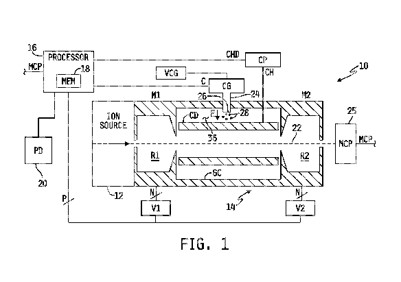
[0008] FIG. 1 is a simplified diagram of an ion mass detection system
including an
embodiment of an electrostatic linear ion trap (ELIT) with control and
measurement
components coupled thereto and including an apparatus for calibrating or
resetting the charge
detector thereof.
[0009] FIG. 2A is a magnified view of the ion mirror M1 of the ELIT
illustrated in FIG. 1
in which the mirror electrodes of M1 are controlled to produce an ion
transmission electric field
therein.
[0010] FIG. 2B is a magnified view of the ion mirror M2 of the ELIT
illustrated in FIG. 1
in which the mirror electrodes of M2 are controlled to produce an ion
reflection electric field
therein.
[0011] FIG. 3A is a plot of charge detection cylinder charge vs. time
illustrating two
different charge detection threshold levels in comparison to a noisy charge
reference on the
charge detection cylinder.
[0012] FIG. 3B is a plot of charge detection cylinder charge vs. time
illustrating a lower
charge detection threshold, as compared with FIG. 3A, in comparison with a
calibrated charge
reference on the charge detection cylinder.
[0013] FIGS. 4A ¨ 4E are simplified diagrams of the ELIT of FIG. 1
demonstrating
sequential control and operation of the ion mirrors and of the charge
generator to calibrate or
reset the charge detector between ion measurement events.
[0014] FIGS. 5A ¨ 5F are simplified diagrams of the ELIT of FIG. 1
demonstrating
control and operation of the charge generator to calibrate or reset the charge
detector between
charge detection events.
[0015] FIG. 6A is a simplified block diagram of an embodiment of an ion
separation
instrument including the ELIT illustrated and described herein and showing
example ion
processing instruments which may form part of the ion source upstream of the
ELIT and/or
which may be disposed downstream of the ELIT to further process ion(s) exiting
the ELIT.
[0016] FIG. 6B is a simplified block diagram of another embodiment of an
ion
separation instrument including the ELIT illustrated and described herein and
showing
example implementation which combines conventional ion processing instruments
with any of
the embodiments of the ion mass detection system illustrated and described
herein.
[0017] FIG. 7 is a simplified flowchart of an embodiment of a process for
controlling the
charge generator of FIG. 1 to selectively induce high frequency charges on the
charge
detection cylinder during normal operation of the ELIT in which mass and
charge of charged
particles are measured thereby, to process the detected high frequency charges
and to use
CA 03100906 2020-11-18
WO 2019/236574
PCT/US2019/035381
- 4 -
information provided thereby to compensate for any drift in gain of the charge
preamplifier over
time.
[0018] FIG. 8 is a plot of the charge detection signal vs. frequency
depicting an
example of the charge detection signal which includes charge peaks
corresponding to
detection of charge induced on the charge detection cylinder of the ELIT by a
charged particle
passing therethrough and additional charge peaks corresponding to detection of
the high
frequency charge simultaneously induced on the charge detection cylinder by
the charge
generator according to the process illustrated in FIG. 7.
[0019] FIG. 9 is a plot of the peak magnitude of the fundamental frequency
of the high
frequency charge induced on the charge detection cylinder by the charge
generator over time.
[0020] FIG. 10 is a plot of an N-sample data set moving average over time
of the peak
magnitude signal illustrated in FIG. 9.
DESCRIPTION OF THE ILLUSTRATIVE EMBODIMENTS
[0021] For the purposes of promoting an understanding of the principles of
this
disclosure, reference will now be made to a number of illustrative embodiments
shown in the
attached drawings and specific language will be used to describe the same.
[0022] This disclosure relates to an electrostatic linear ion trap (ELIT)
including an
apparatus for calibrating or resetting the charge detector thereof, and to
means and methods
for controlling both. In one embodiment, an example of which will be described
in detail below
with respect to FIGS. 3A ¨ 3E, the calibration apparatus is controlled in a
manner which
calibrates or resets the charge detector of the ELIT to a predefined reference
charge level
between ion measurement events. In another embodiment, an example of which
will be
described in detail below with respect to FIGS. 5A ¨ 5F, the calibration
apparatus is controlled
in a manner which calibrates or resets the charge detector of the ELIT to a
predetermined
reference charge level between charge detection events. For purposes of this
disclosure, the
phrase "charge detection event" is defined as detection of a charge associated
with an ion
passing a single time through the charge detector of the ELIT, and the phrase
"ion
measurement event" is defined as a collection of charge detection events
resulting from
oscillation of an ion back and forth through the charge detector a selected
number of times or
for a selected time period.
[0023] Referring to FIG. 1, a charge detection mass spectrometer (CDMS) 10
is shown
including an embodiment of an electrostatic linear ion trap (ELIT) 14 with
control and
measurement components coupled thereto and including an apparatus for
calibrating or
resetting the charge detector of the ELIT 14. In the illustrated embodiment,
the CDMS 10
includes an ion source 12 operatively coupled to an inlet of the ELIT 14. As
will be described
CA 03100906 2020-11-18
WO 2019/236574
PCT/US2019/035381
- 5 -
further with respect to FIG. 6A, the ion source 12 illustratively includes any
conventional device
or apparatus for generating ions from a sample and may further include one or
more devices
and/or instruments for separating, collecting, filtering, fragmenting and/or
normalizing ions
according to one or more molecular characteristics. As one illustrative
example, which should
not be considered to be limiting in any way, the ion source 12 may include a
conventional
electrospray ionization source, a matrix-assisted laser desorption ionization
(MALDI) source or
the like, coupled to an inlet of a conventional mass spectrometer. The mass
spectrometer may
be of any conventional design including, for example, but not limited to a
time-of-flight (TOF)
mass spectrometer, a ref lectron mass spectrometer, a Fourier transform ion
cyclotron
resonance (FTICR) mass spectrometer, a quadrupole mass spectrometer, a triple
quadrupole
mass spectrometer, a magnetic sector mass spectrometer, or the like. In any
case, the ion
outlet of the mass spectrometer is operatively coupled to an ion inlet of the
ELIT 14. The
sample from which the ions are generated may be any biological or other
material.
[0024] In the illustrated embodiment, the ELIT 14 illustratively includes
a charge
detector CD surrounded by a ground chamber or cylinder GC and operatively
coupled to
opposing ion mirrors Ml, M2 respectively positioned at opposite ends thereof.
The ion mirror
M1 is operatively positioned between the ion source 12 and one end of the
charge detector
CD, and ion mirror M2 is operatively positioned at the opposite end of the
charge detector CD.
Each ion mirror Ml, M2 defines a respective ion mirror region R1, R2 therein.
The regions R1,
R2 of the ion mirrors Ml, M2, the charge detector CD, and the spaces between
the charge
detector CD and the ion mirrors Ml, M2 together define a longitudinal axis 22
centrally
therethrough which illustratively represents an ideal ion travel path through
the ELIT 14 and
between the ion mirrors Ml, M2 as will be described in greater detail below.
[0025] In the illustrated embodiment, voltage sources V1, V2 are
electrically connected
to the ion mirrors M1, M2 respectively. Each voltage source V1, V2
illustratively includes one
or more switchable DC voltage sources which may be controlled or programmed to
selectively
produce a number, N, programmable or controllable voltages, wherein N may be
any positive
integer. Illustrative examples of such voltages will be described below with
respect to FIGS.
2A and 2B to establish one of two different operating modes of each of the ion
mirrors M1, M2
as will be described in detail below. In any case, ions move within the ELIT
14 along the
longitudinal axis 22 extending centrally through the charge detector CD and
the ion mirrors M1,
M2 under the influence of electric fields selectively established by the
voltage sources V1, V2.
[0026] The voltage sources V1, V2 are illustratively shown electrically
connected by a
number, P, of signal paths to a conventional processor 16 including a memory
18 having
instructions stored therein which, when executed by the processor 16, cause
the processor 16
to control the voltage sources V1, V2 to produce desired DC output voltages
for selectively
CA 03100906 2020-11-18
WO 2019/236574
PCT/US2019/035381
- 6 -
establishing ion transmission and ion reflection electric fields, TEF, REF
respectively, within
the regions R1, R2 of the respective ion mirrors Ml, M2. P may be any positive
integer. In
some alternate embodiments, either or both of the voltage sources V1, V2 may
be
programmable to selectively produce one or more constant output voltages. In
other
alternative embodiments, either or both of the voltage sources V1, V2 may be
configured to
produce one or more time-varying output voltages of any desired shape. It will
be understood
that more or fewer voltage sources may be electrically connected to the
mirrors Ml, M2 in
alternate embodiments.
[0027] The charge detector CD is illustratively provided in the form of an
electrically
conductive cylinder which is electrically connected to a signal input of a
charge sensitive
preamplifier (or charge sensitive amplifier) CP, and the signal output of the
charge preamplifier
OP is electrically connected to the processor 16. The charge preamplifier OP
is illustratively
operable in a conventional manner to receive a charge signal (CH)
corresponding to a charge
induced on the charge detection cylinder CD by an ion passing therethrough, to
produce a
charge detection signal (CHD) corresponding thereto and to supply the charge
detection signal
CHD to the processor 16. In some embodiments, the charge preamplifier OP may
include
conventional feedback components, e.g., one or more resistors and/or other
conventional
feedback circuitry, coupled between the output and at least one of the inputs
thereof. In some
alternate embodiments, the charge preamplifier OP may not include any
resistive feedback
components, and in still other alternate embodiments the charge preamplifier
OP may not
include any feedback components at all. In any case, the processor 16 is, in
turn, illustratively
operable to receive and digitize charge detection signals CHD produced by the
charge
preamplifier OP, and to store the digitized charge detection signals CHD in
the memory 18.
The processor 16 is further illustratively coupled to one or more peripheral
devices 20 (PD) for
providing signal input(s) to the processor 16 and/or to which the processor 16
provides signal
output(s). In some embodiments, the peripheral devices 20 include at least one
of a
conventional display monitor, a printer and/or other output device, and in
such embodiments
the memory 18 has instructions stored therein which, when executed by the
processor 16,
cause the processor 16 to control one or more such output peripheral devices
20 to display
and/or record analyses of the stored, digitized charge detection signals.
[0028] The voltage sources V1, V2 are illustratively controlled in a
manner, as
described in detail below, which selectively traps an ion entering the ELIT 14
and causes the
trapped ion to oscillate back and forth between the ion mirrors Ml, M2 such
that it repeatedly
passes through the charge detection cylinder CD. A plurality of charge and
oscillation period
values are measured at the charge detection cylinder CD, and the recorded
results are
CA 03100906 2020-11-18
WO 2019/236574
PCT/US2019/035381
- 7 -
processed to determine mass-to-charge ratio, charge and mass values of the ion
trapped in
the ELIT 14.
[0029]
Referring now to FIGS. 2A and 2B, embodiments are shown of the ion mirrors
Ml, M2 respectively of the ELIT 14 depicted in FIG. 1. Illustratively, the ion
mirrors Ml, M2 are
identical to one another in that each includes a cascaded arrangement of 4
spaced-apart,
electrically conductive mirror electrodes. For each of the ion mirrors Ml, M2,
a first mirror
electrode 301 has a thickness W1 and defines a passageway centrally
therethrough of
diameter P1. An endcap 32 is affixed or otherwise coupled to an outer surface
of the first
mirror electrode 301 and defines an aperture Al centrally therethrough which
serves as an ion
entrance and/or exit to and/or from the corresponding ion mirror Ml, M2
respectively. In the
case of the ion mirror Ml, the endcap 32 is coupled to, or is part of, an ion
exit of the ion
source 12 illustrated in FIG. 1. The aperture Al for each endcap 32
illustratively has a
diameter P2.
[0030] A second
mirror electrode 302 of each ion mirror Ml, M2 is spaced apart from
the first mirror electrode 301 by a space having width W2. The second mirror
electrode 302,
like the mirror electrode 301, has thickness W1 and defines a passageway
centrally
therethrough of diameter P2. A third mirror electrode 303 of each ion mirror
Ml, M2 is likewise
spaced apart from the second mirror electrode 302 by a space of width W2. The
third mirror
electrode 302 has thickness W1 and defines a passageway centrally therethrough
of width P1.
[0031] A fourth
mirror electrode 304 is spaced apart from the third mirror electrode 303
by a space of width W2. The fourth mirror electrode 304 illustratively has a
thickness of W1
and is formed by a respective end of the ground cylinder, GC disposed about
the charge
detector CD. The fourth mirror electrode 304 defines an aperture A2 centrally
therethrough
which is illustratively conical in shape and increases linearly between the
internal and external
faces of the ground cylinder GC from a diameter P3 defined at the internal
face of the ground
cylinder GC to the diameter P1 at the external face of the ground cylinder GC
(which is also
the internal face of the respective ion mirror Ml, M2).
[0032] The
spaces defined between the mirror electrodes 301 ¨ 304 may be voids in
some embodiments, i.e., vacuum gaps, and in other embodiments such spaces may
be filled
with one or more electrically non-conductive, e.g., dielectric, materials. The
mirror electrodes
301 ¨ 304 and the endcaps 32 are axially aligned, i.e., collinear, such that a
longitudinal axis 22
passes centrally through each aligned passageway and also centrally through
the apertures
Al, A2. In embodiments in which the spaces between the mirror electrodes 301 -
304 include
one or more electrically non-conductive materials, such materials will
likewise define
respective passageways therethrough which are axially aligned, i.e.,
collinear, with the
passageways defined through the mirror electrodes 301 ¨ 304 and which
illustratively have
CA 03100906 2020-11-18
WO 2019/236574
PCT/US2019/035381
- 8 -
diameters of P2 or greater. Illustratively, P1 > P3> P2, although in other
embodiments other
relative diameter arrangements are possible.
[0033] A region R1 is defined between the apertures Al, A2 of the ion
mirror Ml, and
another region R2 is likewise defined between the apertures Al, A2 of the ion
mirror M2. The
regions R1, R2 are illustratively identical to one another in shape and in
volume.
[0034] As described above, the charge detector CD is illustratively
provided in the form
of an elongated, electrically conductive cylinder positioned and spaced apart
between
corresponding ones of the ion mirrors Ml, M2 by a space of width W3. In on
embodiment,
W1 > W3 > W2, and P1 > P3> P2, although in alternate embodiments other
relative width
arrangements are possible. In any case, the longitudinal axis 22
illustratively extends centrally
through the passageway defined through the charge detection cylinder CD, such
that the
longitudinal axis 22 extends centrally through the combination of the
passageways defined by
the regions R1, R2 of the ion mirrors Ml, M2 and the passageway defined
through the charge
detection cylinder CD. In operation, the ground cylinder GC is illustratively
controlled to
ground potential such that the fourth mirror electrode 304 of each ion mirror
Ml, M2 is at
ground potential at all times. In some alternate embodiments, the fourth
mirror electrode 304 of
either or both of the ion mirrors Ml, M2 may be set to any desired DC
reference potential, or to
a switchable DC or other time-varying voltage source.
[0035] In the embodiment illustrated in FIGS. 2A and 2B, the voltage
sources V1, V2
are each configured to each produce four DC voltages D1 ¨ D4, and to supply
the voltages D1
¨ D4 to a respective one of the mirror electrodes 301 ¨ 304 of the respective
ion mirror Ml, M2.
In some embodiments in which one or more of the mirror electrodes 301 ¨ 304 is
to be held at
ground potential at all times, the one or more such mirror electrodes 301 ¨
304 may
alternatively be electrically connected to the ground reference of the
respective voltage supply
V1, V2 and the corresponding one or more voltage outputs D1 ¨ D4 may be
omitted.
Alternatively or additionally, in embodiments in which any two or more of the
mirror electrodes
301 ¨ 304 are to be controlled to the same non-zero DC values, any such two or
more mirror
electrodes 301 ¨ 304 may be electrically connected to a single one of the
voltage outputs D1 ¨
D4 and superfluous ones of the output voltages D1 ¨ D4 may be omitted.
[0036] Each ion mirror Ml, M2 is illustratively controllable and
switchable, by selective
application of the voltages D1 ¨ D4, between an ion transmission mode (FIG.
2A) in which the
voltages D1 ¨ D4 produced by the respective voltage source V1, V2 establishes
an ion
transmission electric field (TEF) in the respective region R1, R2 thereof, and
an ion reflection
mode (FIG. 2B) in which the voltages D1 ¨ D4 produced by the respect voltage
source V1, V2
establishes an ion reflection electric field (REF) in the respective region
R1, R2 thereof. As
illustrated by example in FIG. 2A, once an ion from the ion source 12 flies
into the region R1 of
CA 03100906 2020-11-18
WO 2019/236574
PCT/US2019/035381
- 9 -
the ion mirror M1 through the inlet aperture Al of the ion mirror Ml, the ion
is focused toward
the longitudinal axis 22 of the ELIT 14 by an ion transmission electric field
TEF established in
the region R1 of the ion mirror M1 via selective control of the voltages D1 ¨
D4 of Vl. As a
result of the focusing effect of the transmission electric field TEF in the
region R1 of the ion
mirror Ml, the ion exiting the region R1 of the ion mirror M1 through the
aperture A2 of the
ground chamber GC attains a narrow trajectory into and through the charge
detector CD, i.e.,
so as to maintain a path of ion travel through the charge detector CD that is
close to the
longitudinal axis 22. An identical ion transmission electric field TEF may be
selectively
established within the region R2 of the ion mirror M2 via like control of the
voltages D1 ¨ D4 of
the voltage source V2. In the ion transmission mode, an ion entering the
region R2 from the
charge detection cylinder CD via the aperture A2 of M2 is focused toward the
longitudinal axis
22 by the ion transmission electric field TEF within the region R2 so that the
ion exits the ion
mirror M2 through the aperture Al thereof.
[0037] As illustrated by example in FIG. 2B, an ion reflection electric
field REF
established in the region R2 of the ion mirror M2 via selective control of the
voltages D1 ¨ D4
of V2 acts to decelerate and stop an ion entering the ion region R2 from the
charge detection
cylinder CD via the ion inlet aperture A2 of M2, to accelerate the ion in the
opposite direction
back through the aperture A2 of M2 and into the end of the charge detection
cylinder CD
adjacent to M2 as depicted by the ion trajectory 42, and to focus the ion
toward the central,
longitudinal axis 22 within the region R2 of the ion mirror M2 so as to
maintain a narrow
trajectory of the ion back through the charge detector CD toward the ion
mirror Ml. An
identical ion reflection electric field REF may be selectively established
within the region R1 of
the ion mirror M1 via like control of the voltages D1 ¨ D4 of the voltage
source V1 . In the ion
reflection mode, an ion entering the region R1 from the charge detection
cylinder CD via the
aperture A2 of M1 is decelerated and stopped by the ion reflection electric
field REF
established within the region R1, then accelerated in the opposite direction
back through the
aperture A2 of M1 and into the end of the charge detection cylinder CD
adjacent to Ml, and
focused toward the central, longitudinal axis 22 within the region R1 of the
ion mirror M1 so as
to maintain a narrow trajectory of the ion back through the charge detector CD
and toward the
ion mirror M2. An ion that traverses the length of the ELIT 14 and is
reflected by the ion
reflection electric field REF in the ion regions R1, R2 in a manner that
enables the ion to
continue traveling back and forth through the charge detection cylinder CD
between the ion
mirrors Ml, M2 as just described is considered to be trapped within the ELIT
14.
[0038] Example sets of output voltages D1 ¨ D4 produced by the voltage
sources V1,
V2 respectively to control a respective one of the ion mirrors Ml, M2 to the
ion transmission
and reflection modes described above are shown in TABLE I below. It will be
understood that
CA 03100906 2020-11-18
WO 2019/236574
PCT/US2019/035381
- 10 -
the following values of D1 ¨ D4 are provided only by way of example, and that
other values of
one or more of D1 ¨ D4 may alternatively be used.
TABLE I
Ion Mirror Operating Mode Output Voltages (volts DC)
Transmission V1: D1 = 0, D2 = 95, D3 = 135, D4 = 0
V2: D1 = 0, D2 = 95, D3 = 135, D4 = 0
Reflection V1: D1 = 190, D2 = 125, D3 = 135, D4 = 0
V2: D1 = 190, D2 = 125, D3 = 135, D4 = 0
[0039] While the ion mirrors Ml, M2 and the charge detection cylinder CD
are
illustrated in FIGS. 1 ¨ 2B as defining cylindrical passageways therethrough,
it will be
understood that in alternate embodiments either or both of the ion mirrors Ml,
M2 and/or the
charge detection cylinder CD may define non-cylindrical passageways
therethrough such that
one or more of the passageway(s) through which the longitudinal axis 22
centrally passes
represents a cross-sectional area and profile that is not circular. In still
other embodiments,
regardless of the shape of the cross-sectional profiles, the cross-sectional
areas of the
passageway defined through the ion mirror M1 may be different from the
passageway defined
through the ion mirror M2.
[0040] The voltage sources V1, V2 are illustratively controlled in a manner
which
selectively establishes ion transmission and ion reflection electric fields in
the region R1 of the
ion mirror M1 and in the region R2 of the ion mirror M2 in a manner which
allows ions to enter
the ELIT 14 from the ion source 12, and which causes an ion to be selectively
trapped within
the ELIT 14 such that the trapped ion repeatedly passes through the charge
detector CD as it
oscillates within the ELIT 14 between the ion mirrors M1 and M2. A charge
induced on the
charge detector CD each time an ion passes therethrough is detected by the
charge
preamplifier CP, and a corresponding charge detection signal (CHD) is produced
by the
charge preamplifier CP. The magnitude and timing of timing of the charge
detection signal
(CHD) produced by the charge preamplifier CP is recorded by the processor 16
for each
charge detection event as this term is defined herein. Each charge detection
event record
illustratively includes an ion charge value, corresponding to a magnitude of
the detected
charge, and an oscillation period value, corresponding to the elapsed time
between charge
detection events, and each charge detection event record is stored by the
processor 16 in the
memory 18. The collection of charge detection events resulting from
oscillation of an ion back
and forth through the charge detector CD a selected number of times or for a
selected time
CA 03100906 2020-11-18
WO 2019/236574
PCT/US2019/035381
- 11 -
period, i.e., a making up an ion measurement event as this term is defined
herein, are then
processed to determine charge, mass-to-charge ratio and mass values of the
ion.
[0041] In one embodiment, the ion measurement event data are processed by
computing, with the processor 16, a Fourier Transform of the recorded
collection of charge
detection events. The processor 16 is illustratively operable to compute such
a Fourier
Transform using any conventional digital Fourier Transform (DFT) technique
such as for
example, but not limited to, a conventional Fast Fourier Transform (FFT)
algorithm. In any
case, the processor 16 is then illustratively operable to compute an ion mass-
to-charge ratio
value (m/z), an ion charge value (z) and ion mass values (m), each as a
function of the
computed Fourier Transform. The processor 16 is illustratively operable to
store the computed
results in the memory 18 and/or to control one or more of the peripheral
devices 20 to display
the results for observation and/or further analysis.
[0042] It is generally understood that the mass-to-charge ratio (m/z) of
an ion
oscillating back and forth through the charge detector CD of an ELIT between
opposing ion
mirrors Ml, M2 thereof is inversely proportional to the square of the
fundamental frequency ff
of the oscillating ion according to the equation:
[0043] rniz = C/ff2,
[0044] where C is a constant that is a function of the ion energy and also
a function of
the dimensions of the respective ELIT, and the fundamental frequency ff is
determined directly
from the computed Fourier Transform. The value of the ion charge, z, is
proportional to the
magnitude FTMAG of the fundamental frequency ff, taking into account the
number of ion
oscillation cycles. In some cases, the magnitude(s) of one or more of the
harmonic
frequencies of the FFT may be added to the magnitude of the fundamental
frequency for
purposes of determining the ion charge, z. In any case, ion mass, m, is then
calculated as a
product of m/z and z. The processor 16 is thus operable to compute m/z =
C/ff2, z =
F(FTMAG) and m = (m/z)(z). Multiple, e.g., hundreds or thousands or more, ion
trapping
events are typically carried out for any particular sample from which the ions
are generated by
the ion source 12, and ion mass-to-charge, ion charge and ion mass values are
determined/computed for each such ion trapping event. The ion mass-to-charge,
ion charge
and ion mass values for such multiple ion trapping events are, in turn,
combined to form
spectral information relating to the sample. Such spectral information may
illustratively take
different forms, examples of which include, but are not limited to, ion count
vs. mass-to-charge
ratio, ion charge vs. ion mass (e.g., in the form of an ion charge/mass
scatter plot), ion count
vs. ion mass, ion count vs. ion charge, or the like.
[0045] Referring again to FIG. 1, the illustrated ELIT 14 further includes
a charge
generator CG electrically connected to the processor 16 and electrically
connected to a charge
CA 03100906 2020-11-18
WO 2019/236574
PCT/US2019/035381
- 12 -
generator voltage source VCG. In the illustrated embodiment, the charge
generator voltage
source VCG is programmable or manually controllable to produce one or more DC
voltages,
voltage pulses and/or voltage waveforms of any magnitude, shape, duration
and/or frequency.
In alternate embodiments, the charge generator voltage source VCG may be
operatively
coupled to the processor 16 so that the processor 16 may control the charge
generator voltage
source VCG to produce one or more DC voltages, voltage pulses and/or voltage
waveforms of
any magnitude, shape, duration and/or frequency. In the illustrated embodiment
at least one
charge outlet passage 24 of the charge generator CG illustratively extends
through the ground
chamber GC such that a charge outlet 26 of the charge outlet passage 24 is in
fluid
communication with a space 36 defined between the inner surface of the ground
chamber GC
and the outer surface of the charge detection cylinder CD. In the illustrated
embodiment, a
single charge outlet passage 24 is shown extending through the ground chamber
GC, although
in alternate embodiments multiple charge outlet passages may extend through
the ground
chamber GC. In such embodiments, two or more charge outlet passages may be
singly
spaced apart, or spaced apart in groups of two or more, axially and/or
radially along the charge
detection cylinder CD.
[0046] In one embodiment, the charge generator CG is configured to be
responsive to
a control signal C produced by the processor 16 to generate free charges 28
which pass
through the charge outlet 26 of the one or more charge outlet passages 24 into
the space 36
defined between the inner surface of the ground chamber or cylinder GC and the
outer surface
of the electrically conductive charge detection cylinder CD. In the
illustrated embodiment, the
charges 28 produced by the charge generator are positive charges, although the
charge
generator CG may in alternate embodiments be configured to produce negative
charges or to
selectively produce positive or negative charges.
[0047] In one embodiment, the charge generator CG is configured, or
controllable
using conventional control circuitry and/or conventional control techniques,
to be responsive to
activation of the control signal C produced by the control circuit 16 to
generate and supply to
the space 36 within the ELIT 14 a predictable number of free charges 28,
within any desired
tolerance level, per unit of time. The unit of time may have any desired
duration. In such
embodiments, the total number of charges 28 supplied by the charge generator
CG to the
space 36 within the ELIT 14 in response to a single activation of the control
signal C is thus
controllable as a function of the number of charges 28 produced by the charge
generator CG
per unit time and a duration, i.e., pulse width, of the active portion of the
control signal C. In
alternate embodiments, the charge generator CG may be configured to produce a
programmable number of charges 28 per unit time. In still other embodiments,
the charge
detector CG may be configured such that the number of charges 28 produced
thereby in
CA 03100906 2020-11-18
WO 2019/236574
PCT/US2019/035381
- 13 -
response to the control signal C is constant and predictable, or programmable,
within any
desired tolerance level, regardless and independently of the duration of the
control signal C. In
such embodiments, the number of charges 28 supplied by the charge generator CG
to the
space 36 within the ELIT 14 in response to any single activation of the
control signal C is thus
constant and predictable, and the total number of charges 28 that may be
supplied by the
charge generator CG to the space 36 within the ELIT 14 is controllable as a
function of the
total number of charges 28 produced with each single activation of the control
signal C and the
total number of activations of the control signal C produced by the processor
16.
[0048] The charge generator CG may be provided in the form of any
conventional
charge generator. As one example, the charge generator CG may be or include a
conventional filament responsive to a voltage or current applied thereto to
generate and
produce the free charges 28. As another example, the charge generator CG may
be or
include an electrically conductive mesh or grid responsive to a voltage or
current applied
thereto to generate and produce the free charges 28. As yet another example,
the charge
generator CG may be or include a particle charge generator configured to
produce the free
charges in the form of charged particles from a sample source. Examples of
such particle
charge generators may include, but are not limited to, an electrospray
ionization (ESI) source,
a matrix-assisted Laser Desorption Ionization (MALDI) source, or the like. In
any case, the
charge generator CG is operable to generate and supply charges to the space 36
within the
ELIT 14 via the charge outlet(s) of the one or more charge outlet passages
extending into,
and/or fluidly coupled to, the space 36.
[0049] With no charge induced on the charge detector CD by a charged
particle
passing therethrough or by one or more free charges 28 produced by the charge
generator
GC, the charge detection cylinder CD illustratively operates at or near a
reference charge level
CHREF. As the charge detection cylinder CD is not powered or grounded, the
reference charge
level CHREF is typically tens of charges (i.e., elementary charges "e") or
less, although in some
applications the reference charge level CHREF may be more than tens of
charges.
[0050] As described above, the charge generator CG is responsive to control
signals C
produced by the processor 16 or other control signal generating circuitry to
generate charges
28 of desired polarity which then pass into the space 36 between the inner
surface of the
ground cylinder GC and the outer surface of the charge detection cylinder CD.
As the ground
cylinder GC is generally maintained at ground potential and the charge
detection cylinder CD
typically operates at or near ground potential, the space 36 is substantially
a field-free region.
In some embodiments, the one or more charge outlet passages 24 and/or the body
of the
charge generator CG illustratively include(s) one or more regions in which an
electric field of
suitable direction is established by the voltage source VCG (or by some other
source(s)) for
CA 03100906 2020-11-18
WO 2019/236574
PCT/US2019/035381
- 14 -
the purpose of accelerating the generated charges 28 into the field free
region 36 so that the
accelerated charges 28 then travel through the field free region 36 toward and
into contact with
the outer surface of the charge detection cylinder CD. When such charges 28
contact the
outer surface of the charge detection cylinder CD, they impart their
respective charges onto
the charge detection cylinder CD. In this regard, the generation of charges 28
by the charge
generator GC, and travel of the generated charges through the field free
region 36 toward and
into contact with the outer surface of the charge detection cylinder to
thereby impart their
charges onto the charge detection cylinder defines a "charge injection"
process via which the
generated charges 28 calibrate or reset the charge detection cylinder CD
and/or the charge
sensitive preamplifier OP in some embodiments thereof. Such injected charges
may
illustratively be removed from the charge detection cylinder CD by applying an
equal amount of
opposite charge, and may therefore illustratively be used to calibrate and/or
reset the charge
detection cylinder in some applications and/or to calibrate or reset the
charge preamplifier in
other applications.
[0051] The "charge injection" process just described is different from a
"charge
induction" process in which charge may be induced on the charge detection
cylinder CD by
establishing a voltage difference between the charge detection cylinder CD and
a voltage
reference, e.g., ground potential. One illustrative technique for inducing
charge on the charge
detection cylinder CD without physically coupling one or more wires and/or one
or more
electronic devices to the charge detection cylinder CD is to configure the
charge generator GC
such that the voltage source VCG establishes a potential of desired polarity
on the at least one
charge outlet passage 24. Establishing a DC potential on the at least one
charge outlet
passage 24 without generating charges 28 will generally create an electric
field between the at
least one charge outlet passage 24 and the charge detection cylinder CD, thus
inducing a DC
voltage and, in turn, a charge on the charge detection cylinder CD. The
magnitude of the
induced charge will generally be dependent upon the strength of the
established electric field
and thus upon the magnitude of the voltage applied by the voltage source VCG
to the at least
one charge outlet passage 24. Such induced charges may illustratively be
removed or
modified by applying a different voltage, e.g., ground or other potential, to
the charge detection
cylinder CD, and may therefore be used to compensate for switching voltages
applied to the
ion mirror(s) M1 and/or M2, and for calibrating the charge preamplifier CP in
some
embodiments thereof. In alternate embodiments of the charge generator CG
described above
in which the charge generator CG is operable to generate free charges, the
charge generator
CG may thus be configured to operate as a charge induction antenna. In such
embodiments,
the voltage source VCG is controlled, illustratively by the processor 16, to
produce a DC
voltage, a voltage pulse or a series of voltage pulses, or a voltage waveform
which is/are
CA 03100906 2020-11-18
WO 2019/236574
PCT/US2019/035381
- 15 -
applied to the charge outlet passage(s) 24 to create or establish one or more
corresponding
electric fields between the charge outlet passage(s) 24 generally (and in some
embodiments
the charge outlet(s) 26 specifically) and the charge detection cylinder CD to
thereby induce a
corresponding charge or charges on the charge detection cylinder. In such
embodiments, the
charge outlet passage(s) 24 may, but need not, include one or more charge
outlets 26 in fluid
communication with the space 36. In some embodiments, for example, in which
the charge
generator CG is configured strictly for charge induction, the charge outlet
passage(s) 24 may
be or include one or more electrically conductive rods, probes, filaments or
the like which
does/do not include any outlets for dispensing or otherwise producing free
charges. In other
embodiments in which the charge generator CG is configured to operate as a
charge induction
device and a charge injection device, the charge outlet passage(s) 24 will
illustratively include
one or more charge outlets 24 as described above for dispensing or otherwise
producing free
charges 28.
[0052] Thus, in some embodiments, the charge generator CG is illustratively
configured to operate strictly as a charge injection device in which the
charge generator CG is
responsive to control signals C to generate charges 28 of suitable polarity
and to accelerate
the generated charges 28 out of the at least one charge outlet 26 of the at
least one charge
outlet passage 24 and into the field free region 36 such that the generated
charges 28 travel
through the field free region 36 toward and into contact with the external
surface of the charge
detection cylinder CD to impart their charges on the charge detection cylinder
CD. In alternate
embodiments, the charge generator CG may illustratively be configured to
operate strictly as a
charge induction device in which the charge generator CG is responsive to
control signals C to
apply at least one voltage of suitable magnitude and polarity to establish a
corresponding
electric field within the region 36 between the at least one charge outlet
passage 24 and the
charge detection cylinder CD to induce a DC voltage, and thus a charge, on the
charge
detection cylinder CD. In other alternate embodiments, the charge generator CD
may
illustratively be configured to operate both (e.g., simultaneously or
separately) as a charge
injection device and as a charge induction device in which the charge
generator CG is
responsive to control signals C produced by the processor 16 to generate
charges 28 of
suitable polarity and/or to apply one or more voltages of suitable magnitude
and polarity to
establish an electric field within the region 36 between the at least one
charge outlet passage
24 and the charge detection cylinder CD to (i) induce a DC voltage, and thus a
charge, on the
charge detection cylinder CD, and (ii) to also accelerate the generated
charges 28, under the
influence of the established electric field within the region 36, toward and
into contact with the
external surface of the charge detection cylinder CD to impart their charges
on the charge
detection cylinder CD. The charge generator CG may thus be configured and
operable strictly
CA 03100906 2020-11-18
WO 2019/236574
PCT/US2019/035381
- 16 -
as a charge injector, strictly as a charge inducer or as a combination charge
injector and
charge inducer.
[0053] In embodiments in which the charge generator CG is configured and
operable
as a charge injector to produce a controlled number of charges 28 which then
travel to, or are
transported to, and in contact with the outer surface of the charge detection
cylinder CD, such
charges illustratively impart a target charge level, CHT, on the charge
detection cylinder CD. In
one embodiment, the number and polarity of the generated charges 28 may be
selected to
impart a target charge level CHT that is greater than CHREF, e.g., to achieve
a constant target
charge level CHT which is above CHREF and any noise induced thereon, and in
other
embodiments the number and polarity of the generated charges 28 may be
selected to impart
a target charge level CHT that is less than CHREF, e.g., to achieve a target
charge level CHT at
or near a zero charge level. In embodiments in which the charge generator CG
is configured
and operable as a charge inducer to controllably establish an electric field
which induces a DC
voltage or potential on the charge detection cylinder CD, such DC voltage or
potential
illustratively induces the target charge level CHT of suitable magnitude and
polarity on the
charge detection cylinder CD. In embodiments in which the charge generator CG
is configured
and operable as a combination charge injector and charge inducer, the net
charge induced
and imparted on the charge detection cylinder is the target charge CHT of
suitable magnitude
and polarity.
[0054] The reference charge level CHREF on the charge detection cylinder
CD is
subject to one or more potentially significant sources of charge noise which
may introduce
uncertainty in charge detection events as a result of uncertainty in the
reference charge level
at any point in time. Referring to FIG. 3A, for example, a plot is shown of
charge CH on the
charge detection cylinder CD vs. time in which no charge detection events are
present but in
which an example charge noise waveform 50 is shown superimposed on the
reference charge
level CHREF. In embodiments in which the charge sensitive preamplifier CP does
not include
feedback components, one such source of such charge noise 50 is an
accumulation of
charges on the charge detection cylinder CD and thus at the input of the
charge sensitive
preamplifier CP during normal operation thereof. In this and other
embodiments, capacitance
of the charge detector CD also contributes, as does spurious noise caused by
external events
and extraneous charges induced on the charge detection cylinder resulting from
switching of
either or both of the ion mirrors Ml, M2 between ion transmission and ion
reflection modes of
operation.
[0055] Such charge noise 50, from any source, is undesirable as it can
produce false
charge detection events and/or can require setting a charge detection
threshold higher than
desired. As an example of the former case, the plot of FIG. 3A further
illustrates an example
CA 03100906 2020-11-18
WO 2019/236574
PCT/US2019/035381
- 17 -
charge detection threshold CHTHi implemented in the ion mass detection system
10 for the
purpose of distinguishing valid charge detection events from the reference
charge level CHREF.
In the illustrated example, two peaks 52, 54 of the charge noise 50 present at
and around
CHREF exceed CHTFH and will thus be incorrectly or falsely detected as valid
charge detection
events, thereby corrupting the ion measurement event data for the ion(s) being
evaluated. As
an example of the latter case, a second example charge detection threshold
CHTH2 is also
illustrated in FIG. 3A which is illustratively positioned safely above the
highest peak of the
charge noise 50 so as to avoid false charge detection events of the type just
described.
However, the higher charge detection threshold CHTH2 leaves an undesirably
large range of
undetectable charge values between CHTH2 and CHREF which would otherwise be
detectable
but for the high level of charge noise 50.
[0056] In the embodiment of the ELIT 14 illustrated in FIG. 1, the charge
generator CG
is illustratively implemented and controlled to selectively generate a target
number of charges
28 which are transported through the field free region 36 to, and into contact
with, the outer
surface of the charge detection cylinder CD, e.g., under the influence of one
or more suitably
directed electric fields at or within the charge generator CG as described
above. The charges
28 deposited on the charge detection cylinder CD illustratively combine with
any charge noise
carried on the charge detection cylinder CD to produce a substantially
constant, predictable
and repeatable target charge level, CHT, on the charge detection cylinder CD.
In one example
embodiment, the target number and polarity of the generated charges 28 may be
selected to
impart a target charge level CHT on the charge detection cylinder which is
greater in magnitude
than the combination of the reference charge level CHREF and any charge noise
present on the
charge detection cylinder CD. The target charge level CHT in this example
embodiment thus
envelopes and overrides the combination of CHREF and any charge noise, leaving
a new and
substantially constant charge reference in the form of CHT. Alternatively or
additionally, the
charge generator CG may be controlled to induce a suitable charge on the
charge detection
cylinder CD by controlling the voltage source VCG to apply one or more
corresponding
voltages to the charge generator CG.
[0057] In alternate embodiments, the target number and polarity of the
generated
charges 28 may be selected to neutralize at least one or the combination of
the reference
charge level CHREF and any charge noise present on the charge detection
cylinder CD so as to
induce a resulting target charge level CHT on the charge detection cylinder CD
which is less
than CHREF, e.g., to achieve a target charge level CHT or near a zero charge
level. Such a
result may illustratively be accomplished by controlling the charge generator
CG to first inject
positive charges and to then inject negative charges, or to alternatively
induce a suitable
charge on the charge detection cylinder CD by controlling the voltage source
VCG to apply
CA 03100906 2020-11-18
WO 2019/236574
PCT/US2019/035381
- 18 -
one or more corresponding voltages to the charge generator CG. In some
embodiments in
which an amount of charge noise 50 at the input charge sensitive preamplifier
OP is
specifically targeted (e.g., in embodiments in which the charge sensitive
preamplifier does not
include any feedback components as described above), the target charge level
CHT may be a
charge magnitude and/or polarity which, when deposited or imparted on the
charge detection
cylinder CD, acts to clear such charge noise 50 therefrom and thus from the
input of the
charge preamplifier so as to reset the charge sensitive preamplifier OP to
predictable operating
conditions.
[0058] In any case, the target number of charges 28 generated by the
charge
generator CG and transported to, and in contact with, the outer surface of the
charge detection
cylinder CD and/or the charge induced on the charge detection cylinder CD by
the operation of
the charge generator CG, operate to set the charge detection cylinder CD to a
substantially
predictable and repeatable target charge level CHT, as illustrated by example
in FIG. 3B. The
target charge level CHT establishes a "new" reference charge level against
which subsequent
charge detection events are measured. As the new reference charge level CHT is
substantially
repeatable, a substantial reduction in the charge difference between a charge
detection
threshold CHTH3 and CHT can be realized as also illustrated in FIG. 3B,
thereby increasing the
range of detectable ion charge as compared with conventional ELITs.
[0059] Referring now to FIGS. 4A ¨ 4E, simplified diagrams of the ELIT 14
of FIG. 1
are shown demonstrating sequential control and operation of the ion mirrors
Ml, M2, as
described above, and of the charge generator CG to calibrate or reset the
charge detection
cylinder CD between ion measurement events. Referring to FIG. 4A, the ELIT 14
has just
concluded an ion measurement event in which an ion was trapped in the ELIT 14
and in which
the processor 16 was operable to control the voltage sources V1, V2 to control
the ion mirrors
Ml, M2 to the ion reflection modes of operation (R) in which ion reflection
electric fields were
established in the regions R1, R2 of each respective ion mirror Ml, M2. The
ion thus
oscillated back and forth between M1 and M2, each time passing through the
charge detection
cylinder CD whereupon the charge induced thereby on the charge detection
cylinder CD was
detected by the charge preamplifier OP and the ion detection event was
recorded by the
processor 16. After the ion had oscillated back and forth through the ELIT 14
between the ion
mirrors Ml, M2 a selected number of times or for a selected time period, the
processor 16 was
operable to control the voltage source V2 to control the ion mirror M2 to the
ion transmission
mode (T) of operation by establishing an ion transmission field within the
region R2 of the ion
mirror M2, while maintaining the ion mirror M1 in the ion reflection mode (R)
of operation as
illustrated in FIG. 4A. As a result, the trapped ion exits the ion mirror M2
via the aperture A2 of
M2 as illustrated by the ion trajectory 60 in FIG. 4A.
CA 03100906 2020-11-18
WO 2019/236574
PCT/US2019/035381
- 19 -
[0060] When the ELIT 14 has been operating in the state illustrate in FIG.
4A for a
selected time period, or for a selected time period in which no charge
detection events occur,
the processor 16 is operable to supply a control signal C to the charge
generator CG to cause
the charge generator CG to controllably generate a target number of free
charges 28 and
supply the free charges 28 to the space 36 defined between the ground cylinder
GC and the
charge detection cylinder CD, as illustrated in FIG. 4B. In charge injection
operation of the
charge generator CG, the generated free charges 28 travel toward, and into
contact with, the
external surface of the charge detection cylinder CD through the field-free
region 36 as
described above. In charge induction operation, an electric field established
by the charge
generator voltage source VCG or other electric field generation structure
induces a charge, on
the charge detection cylinder CD. As the ion mirror M1 has been in the
reflection mode (R) of
operation and the ion mirror M2 has been in the transmission mode (T) of
operation for a time
period sufficient to clear the ELIT 14 of an ions, no ions are transported
through the charge
detection cylinder CD as the free charges 28 are generated and travel to the
charge detection
cylinder CD during charge injection operation. As such, the target number of
charges 28
generated by the charge generator CG contacting the outer surface of the
charge detection
cylinder CD and imparting their charges thereon operate to calibrate or reset
the charge
detection cylinder CD to a substantially constant, predictable and repeatable
target charge
level CHT as described above. In charge induction operation, the charge
induced on the
charge detection cylinder CD by the electric field established by the charge
generator CG may
similarly be used for calibration and/or reset.
[0061] Referring now to FIG. 40, after the charge detection cylinder CD has
been
calibrated to the target charge level CHT, the processor 16 is operable to
control the voltage
source V1 to control the ion mirror M1 to the ion transmission mode of
operation (T) by
establishing an ion transmission field within the region R1 of the ion mirror
Ml, while also
maintaining the ion mirror M2 in the ion transmission mode (T) of operation.
As a result, ions
generated by the ion source 12 and entering the ion mirror M1 are passed
through the ion
mirror Ml, through the charge detection cylinder CD, through the ion mirror M2
and out of the
ion mirror M2 via the aperture Al of the ion mirror M2 as described above and
as illustrated by
the ion trajectory 62 in FIG. 40. In some embodiments, a conventional ion
detector 25, e.g.,
one or more microchannel plate detectors, is positioned adjacent to the ion
exit aperture Al of
the ion mirror M2, and ion detection information provided by the detector 25
to the processor
16 may be used to adjust one or more of the components and/or operating
conditions of the
ELIT 14 to ensure adequate detection of ions passing through the charge
detection cylinder
CD.
CA 03100906 2020-11-18
WO 2019/236574
PCT/US2019/035381
- 20 -
[0062] Referring now to FIG. 4D, after both of the ion mirrors Ml, M2 have
been
operating in ion transmission operating mode for a selected time period, the
processor 16 is
operable to control the voltage source V2 to control the ion mirror M2 to the
ion reflection mode
(R) of operation by establishing an ion reflection field within the region R2
of the ion mirror M2,
while maintaining the ion mirror Ml in the ion transmission mode (T) of
operation as shown.
As a result, ions generated by the ion source 12 and entering the ion mirror
Ml are passed
through the ion mirror Ml, through the charge detection cylinder CD, and into
the ion mirror M2
where they are reflected back into the charge detection cylinder CD by the ion
reflection field
(R) established in the region R2 of M2, as illustrated by the ion trajectory
64 in FIG. 4D.
[0063] Referring now to FIG. 4E, the processor 16 is operable to control
the voltage
source Vi to control the ion mirror Ml to the ion reflection mode (R) of
operation by
establishing an ion reflection field within the region Ri of the ion mirror
Ml, while maintaining
the ion mirror M2 in the ion reflection mode (R) of operation as shown. In one
embodiment,
the processor 16 is illustratively operable, i.e., programmed, to control the
ELIT 14 in a
"random trapping mode" in which the processor 16 is operable to control the
ion mirror Ml to
the reflection mode (R) of operation after the ELIT has been operating in the
state illustrated in
FIG. 4D, i.e., with Ml in ion transmission mode and M2 in ion reflection mode,
for a selected
time period. Until the selected time period has elapsed, the ELIT 14 is
controlled to operate in
the state illustrated in FIG. 4D. In an alternate embodiment, the processor 16
is operable, i.e.,
programmed, to control the ELIT 14 in a "trigger trapping mode" in which the
processor 16 is
operable to control the ion mirror Ml to the reflection mode (R) of operation
until an ion is
detected at the charge detector CD. Until such detection, the ELIT 14 is
controlled to operate
in the state illustrated in FIG. 4D. Detection by the processor 16 of a charge
on the charge
detector CD is indicative of an ion passing through the charge detector CD
toward the ion
mirror Ml or toward the ion mirror M2, and serves as a trigger event which
causes the
processor 16 to control the voltage source Vi to switch the ion mirror Ml to
the ion reflection
mode (R) of operation to thereby trap the ion within the ELIT 14.
[0064] With both of the ion mirrors Ml, M2 controlled to the ion
reflection operating
mode (R), the ion is made to oscillate back and forth between the regions Ri
and R2 of the
respective ion mirrors Mi , M2 by the ion reflection electric fields
established therein, as
described above and as illustrated by the ion trajectory 66 depicted in FIG
4E. In one
embodiment, the processor 16 is operable to maintain the operating state
illustrated in FIG. 4E
until the ion passes through the charge detection cylinder CD a selected
number of times. In
an alternate embodiment, the processor 16 is operable to maintain the
operating state
illustrated in FIG. 4E for a selected time period after controlling Mi to the
ion reflection mode
(R) of operation. When the ion has passed through the charge detection
cylinder CD a
CA 03100906 2020-11-18
WO 2019/236574
PCT/US2019/035381
- 21 -
selected number of times or has oscillated back-and-forth between the ion
mirrors M1, M2 for
a selected period of time, the processor 16 is operable, i.e., programmed, to
control the
voltage source V2 to control the ion mirror M2 to the ion transmission mode
(T) of operation by
establishing an ion transmission field within the region R2 of the ion mirror
M2, while
maintaining the ion mirror M1 in the ion reflection mode (R) of operation as
illustrated in FIG.
4A. The process then repeats for as many times as desired.
[0065] The charge cylinder calibration or reset technique described with
respect to
FIGS. 4A ¨ 4E may alternatively or additionally be implemented with the ELIT
14 between
charge detection events. It will be understood, however, that in such
embodiments dimensions
of the ELIT 14, and the axial lengths of the ion mirrors Ml, M2 in particular,
must be sized to
allow for the activation of and subsequent generation of the free charges 28
by the charge
generator GC, the deposition of the generated free charges 28 on the external
surface of the
charge detection cylinder CD and stabilization of the resulting target charge
level CHT on the
charge detection cylinder CD, and/or of charge inducement on the charge
detection cylinder
CD by a suitably established electric field, all between the time that a
trapped ion traveling
through the ELIT 14 leaves the charge detection cylinder CD and is reflected
back into the
charge detection cylinder by one of the ion mirrors Ml, M2.
[0066] Referring now to FIGS. 5A ¨ 5F, simplified diagrams of the ELIT 14
of FIG. 1
are shown demonstrating sequential control and operation of the ion mirrors
Ml, M2, as
described above, and of the charge generator CG to calibrate or reset the
charge detection
cylinder CD between such charge detection events. Referring to FIG. 5A, a
single ion 70 is
shown traveling through the ELIT 14 at a time Ti in the direction of the arrow
A from the region
R1 of the ion mirror M1 toward the charge detection cylinder CD. As
illustrated in the
accompanying plot of charge CH on the charge detection cylinder CD vs. time,
the detected
charge signal 80 is at the charge reference CHREF. In FIG. 5B, the ion 70 is
shown at a
subsequent time T2 in which it has progressed along the direction A of travel
and entered the
charge detection cylinder CD. The detected charge signal 80 accordingly shows
a step just
prior to T2 indicative of the detected charge induced on the charge detection
cylinder CD by
the ion 70 contained therein. At a further subsequent time T3, the ion 70 has
progressed
further along the direction A of travel and has approached the end of the
charge detection
cylinder CD, as illustrated in FIG. 50. The peak of the charge detection
signal 80 is
accordingly reaching its end at T3.
[0067] At still a further subsequent time T4, the ion 70 still traveling in
the direction A
has just exited the charge detection cylinder CD and is poised to enter the
region R2 of the ion
mirror M2 as illustrated in FIG. 5D. Upon detecting the attendant falling edge
of the charge
detection signal 80 at time T4, i.e., upon detection by the processor 16 of
the absence of the
CA 03100906 2020-11-18
WO 2019/236574
PCT/US2019/035381
- 22 -
charge detection signal that is produced by the charge preamplifier OP when an
ion is passing
through the charge detection cylinder CD and is inducing its charge on the
charge detection
cylinder, the processor 16 is operable to produce the control signal C at time
15 to activate the
charge generator CG as indicated by the rising edge of the control signal 90.
At a subsequent
time 16, the charge generator CG is responsive to the control signal C to
produce a selected
number of free charges 28, and such free charges 28 then travel through the
field-free region
36 and into contact with the exterior surface of the charge detection cylinder
CD to deposit the
target number of free charges 28 thereon. Alternatively or additionally, the
charge generator
CG may be responsive to the control signal C to generate an electric field
between the at least
one charge outlet passage 24 and the charge detection cylinder CD which
induces a
corresponding charge, on the charge detection cylinder CD.
[0068] At a subsequent time 17, the ion reflection electric field (R)
established in the
region R2 of the ion mirror M2 has trapped and reversed the direction of the
ion 70 so that it is
now traveling in the opposite direction B toward the entrance of the charge
detection cylinder
CD adjacent to the ion mirror M2 as illustrated in FIG. 5E. The processor 16
has deactivated
the control signal C at 17 as indicated by the falling edge of the control
signal 90. In response
to deactivation of the control signal C, the charge generator CG has stopped
generating free
charges 28, and the last of the generated charges 28 are shown in FIG. 5E
moving toward the
exterior surface of the charge detection cylinder CD. Alternatively or
additionally, the charge
generator CG may be responsive to the control signal C at 17 to stop
generating the electric
field described above. Thereafter at time 18, the ion 70 traveling in the
direction B has
reentered the charge detection cylinder CD as indicated by the rising edge of
the charge
detection signal 80 at 18 as illustrated in FIG. 5F. Between 17 and 18, the
generated free
charges 28 deposited on the charge detection cylinder CD settle and stabilize
to result in the
target charge level CHT on the charge detection cylinder CD which becomes the
new charge
reference for the charge detection signal 80 as also illustrated in FIG. 5F.
Alternatively or
additionally, calibration or reset may be accomplished via charge induction as
described
above. A process identical to that illustrated in FIGS. 5A ¨ 5F occurs at the
opposite end of
the ELIT 14 and continues with each oscillation of the ion 70 within the ELIT
14 until the ion
mirror M2 is opened to allow the ion 70 to exit the aperture Al thereof.
EXAMPLES
[0069] The following examples are provided to illustrate three specific
applications; one
in which the charge generator CG is controlled to selectively produce free
charges 28 as part
of a charge injection process to deposit or impart a respective net charge on
the charge
detection cylinder CD, one in which the charge generator CG is controlled as
part of a charge
induction process to selectively induce a charge on the charge detection
cylinder, and one in
CA 03100906 2020-11-18
WO 2019/236574
PCT/US2019/035381
- 23 -
which the charge generator CG is controlled as part of a charge preamplifier
calibration
process to selectively induce a high frequency charge on the charge detection
signal during
normal operation of the ELIT in which mass and charge of a charged particle is
measured
thereby, to process the detected high frequency charges and to use the
information provided
thereby to compensate for any drift in gain of the charge preamplifier over
time. It will be
understood that such applications are provided only by way of example, and
should not be
understood to limit the concepts described herein in any way.
[0070] The first example application is specifically targeted at
embodiments in which
the charge sensitive preamplifier does not include any feedback components, or
at least in
which the charge sensitive preamplifier does not include any feedback
components operable
to bleed or otherwise dissipate or remove charges that may build up or
otherwise accumulate
on the charge detection cylinder CD as charges are induced thereon by trapped
ions passing
therethrough. In such embodiments, charge that builds up or accumulates on the
charge
detection cylinder raises the base charge level at the input of the charge
sensitive preamplifier,
thus causing the output of the charge preamplifier to drift upwardly and,
eventually, to the level
of the supply voltage of the charge sensitive preamplifier. In such
embodiments, the charge
generator CG is configured to operate in charge injection mode, and the
processor 16 is
operable to control the charge generator CG to generate free charges 28 of
appropriate
polarity and quantity which, when deposited or imparted on the charge
detection cylinder CD,
counteracts the accumulated or built up charge thereby resetting the charge
level of the charge
detection cylinder CD and the input of the charge sensitive preamplifier to
the reference charge
level CHREF or other selectable charge level.
[0071] The second example application is specifically targeted at
embodiments in
which the charge generator is configured to operate in charge induction mode
to counteract or
at least reduce charges induced on the charge detection cylinder CD by
electric field transients
produced when switching either or both of the ion mirrors Ml, M2 between ion
transmission
and ion reflection modes as described above. Generally, each time the voltage
source V1
and/or V2 is controlled by the processor 16 to modify the respective voltages
applied to the ion
mirror M1 and/or the ion mirror M2 to switch from an ion transmission electric
field TEF to an
ion reflection electric field REF or vice versa, the switching from one
electric field to the other
creates an electric field transient which induces a corresponding transient
charge on the
charge detection cylinder CD. This transient charge, at least in some
instances, saturates the
output of the charge sensitive preamplifier for some period of time, and in
other instances
causes the charge sensitive preamplifier to produce one or more pulses
detectable by the
processor 16. In either instance, such outputs produced by the charge
sensitive preamplifier
do not correspond to charges induced on the charge detection cylinder CD by a
trapped ion
CA 03100906 2020-11-18
WO 2019/236574
PCT/US2019/035381
- 24 -
passing therethrough, and following any such switching of either ion mirror
Ml, M2 or
simultaneously of both ion mirrors Ml, M2 charge detection data collection by
the processor 16
is conventionally paused or delayed for a period of time to allow the
transient charge induced
on the charge detection cylinder CD to dissipate. In this regard, the
processor 16 is operable
in this second example to control the charge generator CG and/or the voltage
source VCG to
produce a counter-pulse each time one or both of the ion mirrors Ml, M2 is/are
switched
between ion transmission and reflection modes, wherein such counter-pulse
induces a charge
on the charge detection cylinder CD equal or approximately equal and opposite
to the transient
charge induced on the charge detection cylinder CD by the switching of the ion
mirror(s) M1
and/or M2 so as to counteract or at least reduce the net transient charge
induced on the
charge detection cylinder by such switching of the ion mirror(s) M1 and/or M2.
Illustratively,
the shape, duration and/or magnitude of the voltage counter-pulse produced by
the voltage
source VCG is controlled to create an electric field between the charge
generator CG and the
charge detection cylinder CD having a corresponding shape, duration and/or
magnitude to
induce a charge on the charge detection cylinder which is equal and opposite
to the transient
charge induced on the charge detection cylinder CD by the switching of the ion
mirror(s) Ml,
M2. Such counter-pulsing by the voltage source VCG illustratively avoids
saturating the
charge preamplifier CP and, in any case, provides for the processing of charge
detection data
following switching of the ion mirror(s) M1 and/or M2 much sooner than in
conventional ELIT
and/or CDMS instruments.
[0072] It will
be understood that the transient charge induced on the charge detection
cylinder CD by the switching of the ion mirror M1 may be different from that
induced by the
switching of the ion mirror M2, either of which may be different from that
induced when
simultaneously switching both ion mirrors Ml, M2, and that any such transient
charges
induced on the charge detection cylinder CD when switching either or both ion
mirrors Ml, M2
from transmission mode to reflection mode may be different than when switching
from
reflection mode to transient mode. The processor 16 may thus be programmed in
this
example application to control the shape, duration and/or magnitude of the
voltage counter-
pulse produced by the voltage source VCG differently, depending upon how and
which of the
ion mirrors Ml, M2 (or both) are being switched, to selectively create an
appropriate electric
field between the charge generator CG and the charge detection cylinder CD
which has a
corresponding shape, duration and/or magnitude to induce a charge on the
charge detection
cylinder which is equal and opposite to any such transient charge being
induced on the charge
detection cylinder CD by such switching of the ion mirror(s) M1 and/or M2.
[0073] The
third example application is specifically targeted at embodiments in which
the charge sensitive preamplifier may be susceptible to drift in gain
overtime, e.g., due to one
CA 03100906 2020-11-18
WO 2019/236574
PCT/US2019/035381
- 25 -
or any combination of, but not limited to, amplifier operating temperature,
amplifier operating
temperature gradients, and signal history. In such embodiments, the charge
generator CG is
illustratively controlled to selectively induce high frequency charges on the
charge detection
cylinder CD during normal operation of the ELIT 14 in which mass and charge of
charged
particles are measured thereby as described herein, to process the detected
high frequency
charges and to use information provided thereby to compensate for any drift in
gain of the
charge sensitive preamplifier OP over time. In this regard, the simplified
flowchart of FIG. 7
illustrates an example process 200 for controlling the charge generator
voltage source VCG
and/or the charge generator CG to continually induce high frequency charges on
the charge
detection cylinder CD and to use the corresponding information in the
resulting charge
detection signals CHD to compensate for gain drift in the charge sensitive
preamplifier over
time. The process 200 is illustratively stored in the memory 18 in the form of
instructions
executable by the processor 16 to control operation of the charge generator
voltage source
VCG and/or the charge generator CG and to process the charge detection signals
CHD as just
described.
[0074] In this regard, the process 200 begins at step 202 where the
processor 16 is
operable to set a counter, j, equal to 1 or some other starting value.
Thereafter at step 204 the
processor 16 is operable to control the voltage source VCG and/or the charge
generator CG to
produce a high frequency voltage of suitable constant or stable magnitude to
create a
corresponding high-frequency electric field between the outlet 26, e.g., in
the form of an
antenna or other suitable structure, of the charge generator CG and the charge
detection
cylinder CD which induces a corresponding high frequency charge on the charge
detection
cylinder CD. The term "high frequency," as used in this embodiment, should be
understood to
mean a frequency that is at least high enough so that the resulting portion of
the frequency
domain charge detection signal CHD during normal operation of the ELIT 14 is
distinguishable
from the portion of CHD resulting from detection of charge induced by a
charged particle, i.e.,
an ion, passing through the charge detection cylinder. In this regard, the
"high frequency"
should at least be higher than the highest oscillation frequency of any ion
oscillating back and
forth in the ELIT 14 as described above. The high frequency voltage produced
by VCG and/or
CG may take any shape, e.g., square, sinusoidal, triangular, etc., and have
any desired duty
cycle. In one example embodiment, which should not be considered limiting in
any way, the
high frequency voltage produced at the antenna 26 is a square wave which, in
the frequency
domain, includes only the fundamental frequency and odd harmonics.
[0075] Following step 204, the process 200 advances to step 206 where the
processor
16 is operable to measure the charge, Cl, induced on the charge detector CD by
the high
frequency signal produced at the antenna 26 by processing the corresponding
charge
CA 03100906 2020-11-18
WO 2019/236574
PCT/US2019/035381
- 26 -
detection signal CHD produced by the charge sensitive preamplifier CP.
Thereafter at step
208, the processor 16 is operable to convert the time-domain charge detection
signal CHD to a
frequency domain charge detection signal, CIF, e.g., using any conventional
signal conversion
technique such a discrete Fourier transform (DFT), fast Fourier transform
(FFT) or other
conventional technique. Thereafter at step 210, the processor 16 is operable
to determine the
peak magnitude, PM, of the fundamental frequency of the charge detection
signal CIF.
Thereafter at step 212, the processor 16 is operable to compare the counter
value, j, to a
target value, N. Generally, N will be the sample size of a data set containing
multiple,
sequentially measured values of PM, and will define the size of a moving
average window
used to track the drift of the charge sensitive preamplifier CP. In this
regard, N may have any
positive value. Generally, lower values of N will produce a more responsive
but less smooth
moving average, and higher values of N will conversely produce a less
responsive but more
smooth moving average. Typically, N will be selected based on the application.
In one
example application, which should not be considered limiting in any way, N is
100, although in
other applications N may be less than 100, several hundred, 1000 or several
thousand.
[0076] If, at step 212, the processor 16 determines that j is less than or
equal to N, the
process 200 advances to step 214 where the processor 16 is operable to add
PM(j) to an N-
sample data set stored in the memory 18. Thereafter at step 216, the processor
is operable to
increment the counter, j, and to then loop back to step 206. If, at step 212,
the processor 216
instead determines that j is greater than N, the process 200 advances to step
218 where the
processor 16 is operable to determine an average, AV, of the N-sample data set
value PM1-N.
In one embodiment, the processor 16 is illustratively operable at step 218 to
compute AV as an
algebraic average of PMi_N, although in alternate embodiments the processor 16
may be
operable at step 218 to compute AV using one or more other conventional
averaging
techniques or processes.
[0077] Steps 202-218 of the process 200 are illustratively executed prior
to operation
of the instrument 10 to measure a spectrum of masses and charges of ions
generated from a
sample as described herein. In this regard, the purpose of steps 202-218 is to
build an N-
sample data set of peak magnitude values PM and to establish a baseline gain
or gain factor,
AV, of the charge sensitive preamplifier OP prior to normal operation of the
ELIT 14 to
measure ion mass and charge as described herein. It will be understood,
however, that in
other embodiments steps 202-218 may be re-executed at any time, e.g.,
randomly, periodically
or selectively, to reestablish the baseline gain or gain factor.
[0078] Following step 218, the processor 16 is illustratively operable
to begin a
CDMS analysis of a sample by the instrument 10 as described herein, e.g., by
controlling the
voltage sources V1 and V2 to measure masses and charges of ions generated from
a sample
CA 03100906 2020-11-18
WO 2019/236574
PCT/US2019/035381
- 27 -
with the ELIT 14. Thereafter at step 222, as such operation of the instrument
10 and ELIT 14
is taking place, and as the charge generator CG is continually controlled to
induce the high
frequency charge HFC on the charge detection cylinder CD, the processor 16 is
operable, for
each charge detection signal CHD produced by the charge sensitive preamplifier
in response
to a charge induced on the charge detection cylinder CD by a charged particle
passing
therethrough, to (a) determine PM, e.g., in accordance with steps 206-210 or
other
conventional process for determining PM, (b) add PM to the N-sample data set
and delete the
oldest PM value so as to advance the N-sample data set "window" by one data
point, (c)
determine a new average, NAV, of the now updated N-sample data set, e.g., in
accordance
with step 218 or other conventional averaging techniques, (d) determine a
charge sensitive
preamplifier gain calibration factor, GCF, as a function of AV and NAV, and
(e) modify the
portion of the charge detection signal CHD produced by the charge sensitive
preamplifier in
response to a charge induced on the charge detection cylinder CD by a charged
particle
passing therethrough as a function of GCF to compensate for any drift in gain
of the charge
sensitive preamplifier CP.
[0079] It will be understood that any of several conventional techniques
may be used
by the processor 16 at step 222(d) to determine GCF. In one embodiment, for
example, GCF
may be the ratio GCF = NAV/AV or GCF = AV/NAV. In other embodiments, AV may be
normalized, e.g., to a value of 1 or some other value, and NAV may be
similarly normalized as
a function of the normalized AV to produce GCF in the form of a normalized
multiplier. Other
techniques will occur to those skilled in the art, and it will be understood
that any such other
techniques are intended to fall within the scope of this disclosure. In any
case, the processor
16 is illustratively operable at step 222(e) to modify the portion of the
charge detection signal
CHD produced by the charge sensitive preamplifier in response to a charge
induced on the
charge detection cylinder CD by a charged particle passing therethrough to
compensate for
any drift in gain of the charge sensitive preamplifier CP by multiplying the
peak magnitude of
this portion of the charge detection signal CH by GCF. Those skilled in the
art will recognize
other techniques for executing step 222(e) to include in GCF other factors
that may affect the
gain of CP, to include one or more weighting values to boost or attenuate the
gain of CP based
on one or more factors, or the like.
[0080] Referring now to FIG. 8, an example plot of CHD vs. frequency is
shown
depicting an example of the charge detection signal CHD processed at step
222(a) which
includes charge peaks 300 corresponding to detection of charge induced on the
charge
detection cylinder CD of the ELIT 14 by a charged particle passing
therethrough and additional
charge peaks 400 corresponding to detection of the high frequency charge HFC
simultaneously induced on the charge detection cylinder CD by the charge
generator CG. As
CA 03100906 2020-11-18
WO 2019/236574
PCT/US2019/035381
- 28 -
described herein, the frequency of the high-frequency charges induced on the
charge
detection cylinder CD by the antenna 26 of the charge generator CG is at least
sufficiently
higher than the oscillation frequency of the charged particle oscillating back
and forth through
the ELIT 14 to enable the two charge sources to be distinguishable from one
another. The
peak magnitude PM of the fundamental frequency of the induced high frequency
charge HFC
determined at step 222(a) of the process 200 is also illustrated in FIG. 8.
[0081] Referring to FIG. 9, an example plot of the peak magnitude PM of
the
fundamental frequency of the high frequency charge HFC induced on the charge
detection
cylinder CG by the charge generator vs. time 410 is shown which includes the
baseline gain
value AV computed at step 218 and which includes an example drift in the gain
of the charge
sensitive preamplifier CP over time during operation of the instrument 10. It
will be understood
that whereas FIG. 9 depicts the gain drift as being linearly increasing over
time, the gain drift
may alternatively be non-linear or piecewise liner and/or may decrease over
time or increase
at times and decrease at others. In any case, the baseline gain value AV
computed at step
218 occurs during the time window W1 between times TO and Ti, step 220 is
executed at time
Ti, and the charge sensitive preamplifier gain drifts thereafter between Ti
and T3. FIG. 9
further depicts progressive movement of the N-sample time window repeatedly
executed at
step 222(b), i.e., with each charge detection signal CHD resulting from a
charge induced on
the charge detection cylinder CD by a charged particle passing therethrough.
One such
example time window W2 is shown extending from midway between TO and Ti to T2,
and
another example time window W3 is shown extending between times T2 and T.
[0082] Referring now to FIG. 10, a plot is shown of an N-sample data set
moving
average (NAV) 420 over time of the peak magnitude signal 410 illustrated in
FIG. 9, as
determined by the processor 16 at step 222(c) of the process 200. In the
illustrated example,
the moving average NAV smooths the peak magnitude signal 410 to a linearly
increasing
function from the baseline gain or gain factor AV. As described above, NAV and
AV are
illustratively used by the processor 16 at steps 222(d) and 222(e) to modify
the portion of the
charge detection signal CHD produced by the charge sensitive preamplifier in
response to a
charge induced on the charge detection cylinder CD by a charged particle
passing
therethrough to compensate for any drift in gain of the charge sensitive
preamplifier CP by
multiplying the peak magnitude of this portion of the charge detection signal
CH by GCF.
[0083] Referring now to FIG. 6A, a simplified block diagram is shown of an
embodiment of an ion separation instrument 100 which may include the ELIT 14
illustrated and
described herein, and which may include the charge detection mass spectrometer
(CDMS) 10
illustrated and described herein, and which may include any number of ion
processing
instruments which may form part of the ion source 12 upstream of the ELIT 14
and/or which
CA 03100906 2020-11-18
WO 2019/236574
PCT/US2019/035381
- 29 -
may include any number of ion processing instruments which may be disposed
downstream of
the ELIT 14 to further process ion(s) exiting the ELIT 14. In this regard, the
ion source 12 is
illustrated in FIG. 6A as including a number, Q, of ion source stages ISi ¨
ISQ which may be or
form part of the ion source 12. Alternatively or additionally, an ion
processing instrument 110
is illustrated in FIG. 6A as being coupled to the ion outlet of the ELIT 14,
wherein the ion
processing instrument 110 may include any number of ion processing stages OSi
¨ OSR,
where R may be any positive integer.
[0084] Focusing on the ion source 12, it will be understood that the
source 12 of ions
entering the ELIT 14 may be or include, in the form of one or more of the ion
source stages ISi
¨ ISQ, one or more conventional sources of ions as described above, and may
further include
one or more conventional instruments for separating ions according to one or
more molecular
characteristics (e.g., according to ion mass, ion mass-to-charge, ion
mobility, ion retention
time, or the like) and/or one or more conventional ion processing instruments
for collecting
and/or storing ions (e.g., one or more quadrupole, hexapole and/or other ion
traps), for filtering
ions (e.g., according to one or more molecular characteristics such as ion
mass, ion mass-to-
charge, ion mobility, ion retention time and the like), for fragmenting or
otherwise dissociating
ions, for normalizing or shifting ion charge states, and the like. It will be
understood that the
ion source 12 may include one or any combination, in any order, of any such
conventional ion
sources, ion separation instruments and/or ion processing instruments, and
that some
embodiments may include multiple adjacent or spaced-apart ones of any such
conventional
ion sources, ion separation instruments and/or ion processing instruments. In
any
implementation which includes one or more mass spectrometers, any one or more
such mass
spectrometers may be implemented in any of the forms described herein.
[0085] Turning now to the ion processing instrument 110, it will be
understood that the
instrument 110 may be or include, in the form of one or more of the ion
processing stages OSi
¨ OSR, one or more conventional instruments for separating ions according to
one or more
molecular characteristics (e.g., according to ion mass, ion mass-to-charge,
ion mobility, ion
retention time, or the like) and/or one or more conventional ion processing
instruments for
collecting and/or storing ions (e.g., one or more quadrupole, hexapole and/or
other ion traps),
for filtering ions (e.g., according to one or more molecular characteristics
such as ion mass, ion
mass-to-charge, ion mobility, ion retention time and the like), for
fragmenting or otherwise
dissociating ions, for normalizing or shifting ion charge states, and the
like. It will be
understood that the ion processing instrument 110 may include one or any
combination, in any
order, of any such conventional ion separation instruments and/or ion
processing instruments,
and that some embodiments may include multiple adjacent or spaced-apart ones
of any such
conventional ion separation instruments and/or ion processing instruments. In
any
CA 03100906 2020-11-18
WO 2019/236574
PCT/US2019/035381
- 30 -
implementation which includes one or more mass spectrometers, any one or more
such mass
spectrometers may be implemented in any of the forms described herein.
[0086] As one specific implementation of the ion separation instrument 100
illustrated
in FIG. 6A, which should not be considered to be limiting in any way, the ion
source 12
illustratively includes 3 stages, and the ion processing instrument 110 is
omitted. In this
example implementation, the ion source stage ISi is a conventional source of
ions, e.g.,
electrospray, MALDI or the like, the ion source stage IS2 is a conventional
ion filter, e.g., a
quadrupole or hexapole ion guide, and the ion source stage IS3 is a mass
spectrometer of any
of the types described above. In this embodiment, the ion source stage IS2 is
controlled in a
conventional manner to preselect ions having desired molecular characteristics
for analysis by
the downstream mass spectrometer, and to pass only such preselected ions to
the mass
spectrometer, wherein the ions analyzed by the ELIT 14 will be the preselected
ions separated
by the mass spectrometer according to mass-to-charge ratio. The preselected
ions exiting the
ion filter may, for example, be ions having a specified ion mass or mass-to-
charge ratio, ions
having ion masses or ion mass-to-charge ratios above and/or below a specified
ion mass or
ion mass-to-charge ratio, ions having ion masses or ion mass-to-charge ratios
within a
specified range of ion mass or ion mass-to-charge ratio, or the like. In some
alternate
implementations of this example, the ion source stage IS2 may be the mass
spectrometer and
the ion source stage IS3 may be the ion filter, and the ion filter may be
otherwise operable as
just described to preselect ions exiting the mass spectrometer which have
desired molecular
characteristics for analysis by the downstream ELIT 14. In other alternate
implementations of
this example, the ion source stage IS2 may be the ion filter, and the ion
source stage IS3 may
include a mass spectrometer followed by another ion filter, wherein the ion
filters each operate
as just described.
[0087] As another specific implementation of the ion separation instrument
100
illustrated in FIG. 6A, which should not be considered to be limiting in any
way, the ion source
12 illustratively includes 2 stages, and the ion processing instrument 110 is
again omitted. In
this example implementation, the ion source stage ISi is a conventional source
of ions, e.g.,
electrospray, MALDI or the like, the ion source stage IS2 is a conventional
mass spectrometer
of any of the types described above. This is the implementation described
above with respect
to FIG. 1 in which the ELIT 14 is operable to analyze ions exiting the mass
spectrometer.
[0088] As yet another specific implementation of the ion separation
instrument 100
illustrated in FIG. 6A, which should not be considered to be limiting in any
way, the ion source
12 illustratively includes 2 stages, and the ion processing instrument 110 is
omitted. In this
example implementation, the ion source stage ISi is a conventional source of
ions, e.g.,
electrospray, MALDI or the like, and the ion processing stage 0S2 is a
conventional single or
CA 03100906 2020-11-18
WO 2019/236574
PCT/US2019/035381
- 31 -
multiple-stage ion mobility spectrometer. In this implementation, the ion
mobility spectrometer
is operable to separate ions, generated by the ion source stage ISi, over time
according to one
or more functions of ion mobility, and the ELIT 14 is operable to analyze ions
exiting the ion
mobility spectrometer. In an alternate implementation of this example, the ion
source 12 may
include only a single stage ISi in the form of a conventional source of ions,
and the ion
processing instrument 110 may include a conventional single or multiple-stage
ion mobility
spectrometer as a sole stage OSi (or as stage OSi of a multiple-stage
instrument 110). In this
alternate implementation, the ELIT 14 is operable to analyze ions generated by
the ion source
stage ISi, and the ion mobility spectrometer OSi is operable to separate ions
exiting the ELIT
14 over time according to one or more functions of ion mobility. As another
alternate
implementation of this example, single or multiple-stage ion mobility
spectrometers may follow
both the ion source stage ISi and the ELIT 14. In this alternate
implementation, the ion
mobility spectrometer following the ion source stage ISi is operable to
separate ions,
generated by the ion source stage ISi, over time according to one or more
functions of ion
mobility, the ELIT 14 is operable to analyze ions exiting the ion source stage
ion mobility
spectrometer, and the ion mobility spectrometer of the ion processing stage
OSi following the
ELIT 14 is operable to separate ions exiting the ELIT 14 over time according
to one or more
functions of ion mobility. In any implementations of the embodiment described
in this
paragraph, additional variants may include a mass spectrometer operatively
positioned
upstream and/or downstream of the single or multiple-stage ion mobility
spectrometer in the
ion source 12 and/or in the ion processing instrument 110.
[0089] As still another specific implementation of the ion separation
instrument 100
illustrated in FIG. 6A, which should not be considered to be limiting in any
way, the ion source
12 illustratively includes 2 stages, and the ion processing instrument 110 is
omitted. In this
example implementation, the ion source stage ISi is a conventional liquid
chromatograph, e.g.,
HPLC or the like configured to separate molecules in solution according to
molecule retention
time, and the ion source stage IS2 is a conventional source of ions, e.g.,
electrospray or the
like. In this implementation, the liquid chromatograph is operable to separate
molecular
components in solution, the ion source stage IS2 is operable to generate ions
from the solution
flow exiting the liquid chromatograph, and the ELIT 14 is operable to analyze
ions generated
by the ion source stage IS2. In an alternate implementation of this example,
the ion source
stage ISi may instead be a conventional size-exclusion chromatograph (SEC)
operable to
separate molecules in solution by size. In another alternate implementation,
the ion source
stage ISi may include a conventional liquid chromatograph followed by a
conventional SEC or
vice versa. In this implementation, ions are generated by the ion source stage
IS2 from a twice
separated solution; once according to molecule retention time followed by a
second according
CA 03100906 2020-11-18
WO 2019/236574
PCT/US2019/035381
- 32 -
to molecule size, or vice versa. In any implementations of the embodiment
described in this
paragraph, additional variants may include a mass spectrometer operatively
positioned
between the ion source stage IS2 and the ELIT 14.
[0090] Referring now to FIG. 6B, a simplified block diagram is shown of
another
embodiment of an ion separation instrument 120 which illustratively includes a
multi-stage
mass spectrometer instrument 130 and which also includes the charge detection
mass
spectrometer (CDMS) 10 illustrated and described herein implemented as a high-
mass ion
analysis component. In the illustrated embodiment, the multi-stage mass
spectrometer
instrument 130 includes an ion source (IS) 12, as illustrated and described
herein, followed by
and coupled to a first conventional mass spectrometer (MS1) 132, followed by
and coupled to
a conventional ion dissociation stage (ID) 134 operable to dissociate ions
exiting the mass
spectrometer 132, e.g., by one or more of collision-induced dissociation
(CID), surface-induced
dissociation (SID), electron capture dissociation (ECD) and/or photo-induced
dissociation (PID)
or the like, followed by an coupled to a second conventional mass spectrometer
(M52) 136,
followed by a conventional ion detector (D) 138, e.g., such as a microchannel
plate detector or
other conventional ion detector. The CDMS 10 is coupled in parallel with and
to the ion
dissociation stage 134 such that the CDMS 10 may selectively receive ions from
the mass
spectrometer 136 and/or from the ion dissociation stage 132.
[0091] MS/MS, e.g., using only the ion separation instrument 130, is a
well-established
approach where precursor ions of a particular molecular weight are selected by
the first mass
spectrometer 132 (MS1) based on their m/z value. The mass selected precursor
ions are
fragmented, e.g., by collision-induced dissociation, surface-induced
dissociation, electron
capture dissociation or photo-induced dissociation, in the ion dissociation
stage 134. The
fragment ions are then analyzed by the second mass spectrometer 136 (M52).
Only the m/z
values of the precursor and fragment ions are measured in both MS1 and M52.
For high mass
ions, the charge states are not resolved and so it is not possible to select
precursor ions with a
specific molecular weight based on the m/z value alone. However, by coupling
the instrument
130 to the CDMS 10, it is possible to select a narrow range of m/z values and
then use the
CDMS 10 to determine the masses of the m/z selected precursor ions. The mass
spectrometers 132, 136 may be, for example, one or any combination of a
magnetic sector
mass spectrometer, time-of-flight mass spectrometer or quadrupole mass
spectrometer,
although in alternate embodiments other mass spectrometer types may be used.
In any case,
the m/z selected precursor ions with known masses exiting MS1 can be
fragmented in the ion
dissociation stage 134, and the resulting fragment ions can then be analyzed
by M52 (where
only the m/z ratio is measured) and/or by the CDMS instrument 10 (where the
m/z ratio and
charge are measured simultaneously). Low mass fragments, i.e., dissociated
ions of precursor
CA 03100906 2020-11-18
WO 2019/236574
PCT/US2019/035381
- 33 -
ions having mass values below a threshold mass value, e.g., 10,000 Da (or
other mass value),
can thus be analyzed by conventional MS, using MS2, while high mass fragments
(where the
charge states are not resolved), i.e., dissociated ions of precursor ions
having mass values at
or above the threshold mass value, can be analyzed by CDMS 10.
[0092] It will be understood that the dimensions of the various components
of the ELIT
14 and the magnitudes of the electric fields established therein, as
implemented in any of the
systems 10, 100, 120 illustrated in the attached figures and described above,
may illustratively
be selected so as to establish a desired duty cycle of ion oscillation within
the ELIT 14,
corresponding to a ratio of time spent by an ion in the charge detection
cylinder CD and a total
time spent by the ion traversing the combination of the ion mirrors Ml, M2 and
the charge
detection cylinder CD during one complete oscillation cycle. For example, a
duty cycle of
approximately 50% may be desirable for the purpose of reducing noise in
fundamental
frequency magnitude determinations resulting from harmonic frequency
components of the
measured signals. Details relating to such dimensional and operational
considerations for
achieving a desired duty cycle, e.g., such as 50%, are illustrated and
described in co-pending
U.S. Patent Application Ser. No. 62/616,860, filed January 12, 2018, co-
pending U.S. Patent
Application Ser. No. 62/680,343, filed June 4, 2018 and co-pending
International Patent
Application No. PCT/US2019/013251, filed January 11, 2019, all entitled
ELECTROSTATIC
LINEAR ION TRAP DESIGN FOR CHARGE DETECTION MASS SPECTROMETRY, the
disclosures of which are all expressly incorporated herein by reference in
their entireties.
[0093] It will be further understood that one or more charge detection
optimization
techniques may be used with the ELIT 14 in any of the systems 10, 100, 120,
e.g., for trigger
trapping or other charge detection events. Examples of some such charge
detection
optimization techniques are illustrated and described in co-pending U.S.
Patent Application
Ser. No. 62/680,296, filed June 4, 2018 and in co-pending International Patent
Application No.
PCT/US2019/013280, filed January 11, 2019, both entitled APPARATUS AND METHOD
FOR
CAPTURING IONS IN AN ELECTROSTATIC LINEAR ION TRAP, the disclosures of which
are
both expressly incorporated herein by reference in their entireties.
[0094] It will be still further understood that the charge detection
cylinder calibration or
reset apparatus and techniques illustrated in the attached figures and
described herein may be
used in each of two or more ELITs and/or in each of two or more ELIT regions
in applications
which include at least one ELIT array having two or more ELITs or having two
or more ELIT
regions. Examples of some such ELITs and/or ELIT arrays are illustrated and
described in co-
pending U.S. Patent Application Ser. No. 62/680,315, filed June 4, 2018 and in
co-pending
International Patent Application No. PCT/US2019/013283, filed January 11,
2019, both entitled
ION TRAP ARRAY FOR HIGH THROUGHPUT CHARGE DETECTION MASS
CA 03100906 2020-11-18
WO 2019/236574
PCT/US2019/035381
- 34 -
SPECTROMETRY, the disclosures of which are both expressly incorporated herein
by
reference in their entireties.
[0095] It will be further understood that one or more ion source
optimization
apparatuses and/or techniques may be used with one or more embodiments of the
ion source
12 as part of or in combination with any of the systems 10, 100, 120
illustrated in the attached
figures and described herein, some examples of which are illustrated and
described in co-
pending U.S. Patent Application Ser. No. 62/680,223, filed June 4, 2018 and
entitled HYBRID
ION FUNNEL-ION CARPET (FUNPET) ATMOSPHERIC PRESSURE INTERFACE FOR
CHARGE DETECTION MASS SPECTROMETRY, and in co-pending International Patent
Application No. PCT/U52019/013274, filed January 11,2019 and entitled
INTERFACE FOR
TRANSPORTING IONS FROM AN ATMOSPHERIC PRESSURE ENVIRONMENT TO A LOW
PRESSURE ENVIRONMENT, the disclosures of which are both expressly incorporated
herein
by reference in their entireties.
[0096] It will be still further understood that any of the systems 10,
100, 120 illustrated
in the attached figures and described herein may be implemented in or as part
of systems
configured to operate in accordance with real-time analysis and/or real-time
control
techniques, some examples of which are illustrated and described in co-pending
U.S. Patent
Application Ser. No. 62/680,245, filed June 4, 2018 and co-pending
International Patent
Application No. PCT/U52019/013277, filed January 11,2019, both entitled CHARGE
DETECTION MASS SPECTROMETRY WITH REAL TIME ANALYSIS AND SIGNAL
OPTIMIZATION, the disclosures of which are both expressly incorporated herein
by reference
in their entireties.
[0097] It will be still further understood that in any of the systems 10,
100, 120
illustrated in the attached figures and described herein, the ELIT 14 may be
replaced with an
orbitrap, and that the charge detection cylinder calibration or reset
apparatus and techniques
illustrated in the attached figures and described herein may be used with such
an orbitrap. An
example of one such orbitrap is illustrated and described in co-pending U.S.
Patent Application
Ser. No. 62/769,952, filed November 20, 2018 and in co-pending International
Patent
Application No. PCT/US2019/013278, filed January 11, 2019, both entitled
ORBITRAP FOR
SINGLE PARTICLE MASS SPECTROMETRY, the disclosures of which are both expressly
incorporated herein by reference in their entireties.
[0098] It will be yet further understood that one or more ion inlet
trajectory control
apparatuses and/or techniques may be used with the ELIT 14 of any of the
systems 10, 100,
120 illustrated in the attached figures and described herein to provide for
simultaneous
measurements of multiple individual ions within the ELIT 14. Examples of some
such ion inlet
trajectory control apparatuses and/or techniques are illustrated and described
in co-pending
CA 03100906 2020-11-18
WO 2019/236574
PCT/US2019/035381
- 35 -
U.S. Patent Application Ser. No. 62/774,703, filed December 3, 2018 and in co-
pending
International Patent Application No. PCT/US2019/013285, filed January 11,
2019, both entitled
APPARATUS AND METHOD FOR SIMULTANEOUSLY ANALYZING MULTIPLE IONS WITH
AN ELECTROSTATIC LINEAR ION TRAP, the disclosures of which are both expressly
incorporated herein by reference in their entireties.
[0099] While this disclosure has been illustrated and described in detail
in the
foregoing drawings and description, the same is to be considered as
illustrative and not
restrictive in character, it being understood that only illustrative
embodiments thereof have
been shown and described and that all changes and modifications that come
within the spirit of
this disclosure are desired to be protected. For example, it will be
understood that the ELIT 14
illustrated in the attached figures and described herein is provided only by
way of example,
and that the concepts, structures and techniques described above may be
implemented
directly in ELITs of various alternate designs. Any such alternate ELIT design
may, for
example, include any one or combination of two or more ELIT regions, more,
fewer and/or
differently-shaped ion mirror electrodes, more or fewer voltage sources, more
or fewer DC or
time-varying signals produced by one or more of the voltage sources, one or
more ion mirrors
defining additional electric field regions, or the like. As another example,
while the concepts,
structures and/or techniques of this disclosure have been described as being
implemented in
an electrostatic linear ion trap (ELIT), it will be understood that such
concepts, structures
and/or techniques are not intended to be limited to ELITs or variants thereof,
but rather are
intended to be applicable to any conventional charge detector or charge
detection apparatus.
Accordingly, any conventional charge detector or charge detection apparatus
implementing the
concepts, structures and/or techniques illustrated in the attached figures and
described herein
are intended to fall within the scope of this disclosure.